EP3224079B1 - Wechselrichter mit verbesserter sicherheit - Google Patents
Wechselrichter mit verbesserter sicherheit Download PDFInfo
- Publication number
- EP3224079B1 EP3224079B1 EP15820211.9A EP15820211A EP3224079B1 EP 3224079 B1 EP3224079 B1 EP 3224079B1 EP 15820211 A EP15820211 A EP 15820211A EP 3224079 B1 EP3224079 B1 EP 3224079B1
- Authority
- EP
- European Patent Office
- Prior art keywords
- switches
- processing unit
- inverter
- malfunction
- power supply
- Prior art date
- Legal status (The legal status is an assumption and is not a legal conclusion. Google has not performed a legal analysis and makes no representation as to the accuracy of the status listed.)
- Active
Links
Images



Classifications
-
- B—PERFORMING OPERATIONS; TRANSPORTING
- B60—VEHICLES IN GENERAL
- B60L—PROPULSION OF ELECTRICALLY-PROPELLED VEHICLES; SUPPLYING ELECTRIC POWER FOR AUXILIARY EQUIPMENT OF ELECTRICALLY-PROPELLED VEHICLES; ELECTRODYNAMIC BRAKE SYSTEMS FOR VEHICLES IN GENERAL; MAGNETIC SUSPENSION OR LEVITATION FOR VEHICLES; MONITORING OPERATING VARIABLES OF ELECTRICALLY-PROPELLED VEHICLES; ELECTRIC SAFETY DEVICES FOR ELECTRICALLY-PROPELLED VEHICLES
- B60L3/00—Electric devices on electrically-propelled vehicles for safety purposes; Monitoring operating variables, e.g. speed, deceleration or energy consumption
- B60L3/0023—Detecting, eliminating, remedying or compensating for drive train abnormalities, e.g. failures within the drive train
- B60L3/003—Detecting, eliminating, remedying or compensating for drive train abnormalities, e.g. failures within the drive train relating to inverters
-
- H—ELECTRICITY
- H02—GENERATION; CONVERSION OR DISTRIBUTION OF ELECTRIC POWER
- H02H—EMERGENCY PROTECTIVE CIRCUIT ARRANGEMENTS
- H02H7/00—Emergency protective circuit arrangements specially adapted for specific types of electric machines or apparatus or for sectionalised protection of cable or line systems, and effecting automatic switching in the event of an undesired change from normal working conditions
- H02H7/10—Emergency protective circuit arrangements specially adapted for specific types of electric machines or apparatus or for sectionalised protection of cable or line systems, and effecting automatic switching in the event of an undesired change from normal working conditions for converters; for rectifiers
- H02H7/12—Emergency protective circuit arrangements specially adapted for specific types of electric machines or apparatus or for sectionalised protection of cable or line systems, and effecting automatic switching in the event of an undesired change from normal working conditions for converters; for rectifiers for static converters or rectifiers
- H02H7/122—Emergency protective circuit arrangements specially adapted for specific types of electric machines or apparatus or for sectionalised protection of cable or line systems, and effecting automatic switching in the event of an undesired change from normal working conditions for converters; for rectifiers for static converters or rectifiers for inverters, i.e. DC/AC converters
- H02H7/1225—Emergency protective circuit arrangements specially adapted for specific types of electric machines or apparatus or for sectionalised protection of cable or line systems, and effecting automatic switching in the event of an undesired change from normal working conditions for converters; for rectifiers for static converters or rectifiers for inverters, i.e. DC/AC converters responsive to internal faults, e.g. shoot-through
-
- H—ELECTRICITY
- H02—GENERATION; CONVERSION OR DISTRIBUTION OF ELECTRIC POWER
- H02M—APPARATUS FOR CONVERSION BETWEEN AC AND AC, BETWEEN AC AND DC, OR BETWEEN DC AND DC, AND FOR USE WITH MAINS OR SIMILAR POWER SUPPLY SYSTEMS; CONVERSION OF DC OR AC INPUT POWER INTO SURGE OUTPUT POWER; CONTROL OR REGULATION THEREOF
- H02M1/00—Details of apparatus for conversion
- H02M1/32—Means for protecting converters other than automatic disconnection
-
- H—ELECTRICITY
- H02—GENERATION; CONVERSION OR DISTRIBUTION OF ELECTRIC POWER
- H02P—CONTROL OR REGULATION OF ELECTRIC MOTORS, ELECTRIC GENERATORS OR DYNAMO-ELECTRIC CONVERTERS; CONTROLLING TRANSFORMERS, REACTORS OR CHOKE COILS
- H02P29/00—Arrangements for regulating or controlling electric motors, appropriate for both AC and DC motors
- H02P29/02—Providing protection against overload without automatic interruption of supply
- H02P29/024—Detecting a fault condition, e.g. short circuit, locked rotor, open circuit or loss of load
- H02P29/0243—Detecting a fault condition, e.g. short circuit, locked rotor, open circuit or loss of load the fault being a broken phase
-
- Y—GENERAL TAGGING OF NEW TECHNOLOGICAL DEVELOPMENTS; GENERAL TAGGING OF CROSS-SECTIONAL TECHNOLOGIES SPANNING OVER SEVERAL SECTIONS OF THE IPC; TECHNICAL SUBJECTS COVERED BY FORMER USPC CROSS-REFERENCE ART COLLECTIONS [XRACs] AND DIGESTS
- Y02—TECHNOLOGIES OR APPLICATIONS FOR MITIGATION OR ADAPTATION AGAINST CLIMATE CHANGE
- Y02T—CLIMATE CHANGE MITIGATION TECHNOLOGIES RELATED TO TRANSPORTATION
- Y02T10/00—Road transport of goods or passengers
- Y02T10/60—Other road transportation technologies with climate change mitigation effect
- Y02T10/64—Electric machine technologies in electromobility
Definitions
- the present invention relates to the field of inverters and in particular to power inverters used in motor vehicles.
- inverters are used in electric or hybrid vehicles to convert the direct current supplied by batteries, generally high voltage, into alternating current to power the electric motor.
- Another solution consists in doubling certain elements linked to the control electronics and in using “OR” logic functions to generate a command in the event of a malfunction of one of the two elements.
- OR logic functions
- the doubling of the elements linked to the control electronics entails an additional cost and can pose synchronization problems if two elements have to send a message simultaneously following a malfunction.
- the subject of the present invention is therefore an inverter according to claim 1 and a method according to claim 19.
- the use of two power sources to independently power the high side and the low side of the inverter combined with the use of two logic components placed respectively on the high side and the low side allows to be able to short-circuit the switches on the high or low side of the inverter in the event of a malfunction of one of the inverter elements.
- the short-circuiting of the switches on one side of the inverter makes it possible to control the electromotive force created by the magnets of the rotor and thus to put the electric motor and therefore the vehicle in freewheel.
- the short-circuiting of the first switches corresponds to a closing of the first switches and an opening of the second switches; and the short-circuiting of the second switches corresponds to a closing of the second switches and an opening of the first switches.
- the inverter also comprises a processing unit intended to communicate on the one hand with a control unit and on the other hand with the first and the second logic component.
- the processing unit is configured to detect a malfunction of an element of the high side or the low side.
- the inverter also comprises a plurality of comparators whose inputs are connected respectively to the midpoints of the branches and whose outputs are connected to the processing unit, the comparators being configured to compare a electrical quantity from their respective midpoint to a value which depends on the configuration of the switches, the processing unit being configured to detect a malfunction of an element on the high side or on the low side from a difference between said quantity electrical and said value.
- the processing unit is configured to detect a malfunction of an element on the high side, respectively of an element on the low side, from control signals sent by said logic component on the high side, respectively by said logic component on the low side.
- the logic components on the high side and / or on the low side are configured to detect a malfunction of the processing unit from control signals sent by said processing unit.
- the processing unit is configured to control the short-circuiting of the first or second switches as a function of a malfunction of an element on the high side or on the low side.
- the logic components on the low side and on the high side are configured to control the short-circuiting of the second, respectively of the first, switches in the event of a malfunction of the processing unit.
- control unit is included in the inverter.
- control unit is configured to detect a malfunction of the processing unit, and / or the processing unit is configured to detect a malfunction of the control unit.
- control unit is configured to detect a malfunction of the processing unit from control signals sent by said processing unit, and / or the processing unit is configured to detect a malfunction. of the control unit from control signals sent by said control unit.
- the processing unit or the control unit are configured to control the short-circuiting of the second, or the first, switches in the event of a malfunction.
- control unit or the processing unit are configured to control the short-circuiting of the first or second switches by means of permission signals making it possible to activate or deactivate the first or second. switches.
- control unit is configured to send permission signals to the high side to enable or disable the switches on the high side
- processing unit is configured to send permission signals to the high side.
- the low side to activate or deactivate the switches on the low side; or the control unit is configured to send permission signals to the low side to enable or disable the low side switches, and the processing unit is configured to send permission signals to the high side to enable '' activate or deactivate the switches on the high side.
- the processing unit is a separate element from the control unit.
- the inverter is configured to supply an electric motor of a motor vehicle from the first power source or from the second power source.
- the high side comprises first control units
- the low side comprises second control units
- the first and second switches being controlled respectively via the first and the second control units.
- control signals are monitoring signals or error signals.
- the processing unit and the control unit are both powered by the first, respectively the second, power source.
- the processing unit is supplied by the first, respectively the second, power source; and the control unit is powered by the second, respectively the first, power source.
- the present invention also relates to a method for controlling an inverter according to claim 19, in which in the event of a malfunction of the processing unit, the first logic component, respectively the second logic component, detects said malfunction of the processing unit. from the control signals sent by said processing unit and controls the short-circuiting of the first, respectively of the second, switches.
- the present invention also relates to a method for controlling an inverter according to the invention in which, in the event of a malfunction of an element on the high side or of an element on the low side, the processing unit detects said malfunction and controls short-circuiting the first switches or the second switches depending on the type of malfunction.
- the present invention further relates to a method for controlling an inverter according to the invention in which, in the event of a malfunction of the control unit, the processing unit detects said malfunction of the control unit from the signals. signals sent by the control unit and commands the short-circuiting of the first or second switches.
- the present invention also relates to a method of controlling an inverter according to the invention in which the processing unit and the control unit are both supplied by the first, respectively the second, power source and in which in the event of a malfunction of the first, respectively of the second, power source, the second, respectively the first, logic component controls the short-circuiting of the second, respectively of the first, switches.
- the present invention also relates to a method for controlling an inverter according to the invention in which the processing unit is powered by the first, respectively the second, power source, and the control unit is powered by the second, respectively the first power source; and in the event of a malfunction of the power source supplying the control unit, the processing unit controls the short-circuiting of the switches supplied by its power source; and in the event of a malfunction of the power source supplying the processing unit, the logic component supplied by the other supply source controls the short-circuiting of the switches supplied by this other supply source.
- the present invention relates to an inverter and the associated control method.
- the figure 1 represents a diagram of an example of an inverter 1 comprising three branches denoted B1, B2 and B3 respectively, mounted in parallel between a first connection point denoted C1 and a second connection point denoted C2.
- Each branch B1, B2 and B3 comprises a first switch 3 connected to the first connection point C1 mounted in series with a second switch 3 'connected to the second connection point C2.
- the first switches 3 are distributed over a high side of the inverter 1 denoted HS while the second switches 3 'are distributed over a low side of the inverter 1 denoted LS.
- the midpoints of the branches denoted R, S and T are connected to the phases of the electric motor to be supplied.
- the first connection point C1 is for example connected to a high potential of an energy source intended to supply energy to, or receive energy from, the electric motor via the inverter 1
- the second connection point C2 is for example connected to a low potential of this energy source.
- the inverter 1 will be a three-phase H-bridge inverter, however, the present invention is not limited to a three-phase H-bridge inverter but also extends to other multi-phase inverter structures. .
- the switches 3, 3 ' are here represented by transistors, for example insulated gate bipolar transistors ("Insulated Gate bipolar transistor (IGBT)” or metal-oxide gate field effect transistors (“Metal Oxide Semiconductor Field Effect Transistor (MOSFET) ”but the present invention is not limited to this type of transistors but extends to all types of switches.
- IGBT Insulated Gate bipolar transistor
- MOSFET Metal Oxide Semiconductor Field Effect Transistor
- the high HS and low LS sides of the inverter 1 also respectively comprise a first logic component 5 dedicated to driving the first switches 3 and a second logic component 5 'dedicated to driving the second switches 3'.
- These logic components 5 and 5 ′ are for example complex programmable logic circuits or networks (“Complex Programmable Logic Device (CPLD)” or integrated circuits with specific application (“Application Specific Integrated Circuit (ASIC)” in English). .
- CPLD Complex Programmable Logic Device
- ASIC Application Specific Integrated Circuit
- these logic components 5 and 5 ′ can also be microcontrollers or in-situ programmable gate arrays (“Field Programmable Gate Array (FPGA)”.
- the first logic component 5 can individually control the opening or closing of the first switches 3 while the second logic component 5 'can individually control the opening or closing of the second switches 3'.
- the first 5 and the second 5 ′ logic component only transmit the opening and closing commands respectively to the first 3 and to the second 3 ′ switches, coming for example from a control unit described later.
- the elements dedicated to controlling the high side switches HS are supplied by a first power source (not shown) while the elements dedicated to controlling the low side switches LS (second switches) are supplied by a second source d power supply (not shown) independent of the first power source.
- the second power source will correspond to this motor power supply battery, also called traction battery, for example.
- a high voltage battery greater than 100V for example
- the first power source will correspond to a second battery, for example an accessory power supply battery (12V for example).
- the use of the two logic components 5 and 5 'and of two independent power sources distributed on the high side HS and the low side LS of the inverter 1 makes it possible to be able to control at least the first 3 or the second 3 'switches in the event of a malfunction of one of the logic components 5 or 5' or of one of the power sources.
- Each switch 3 and 3 'of the inverter 1 is associated with a control unit ("driver" in English) denoted 7 for the first switches and 7' for the second switches, said control units 7 and 7 'being supplied respectively. by the first 15 and the second 17 power source.
- a potential barrier 9 can be placed at the level of the control units 7, 7 'which allows electrical insulation, in particular between the high voltage and low voltage masses, to reinforce the protection of people.
- the control units 7 and 7 ' are respectively connected to the first and to the second logic component 5 and 5'.
- the inverter 1 also comprises a processing unit 11 connected to the first and to the second logic component 5 and 5 'and intended to communicate with a control unit 13.
- the processing unit 11 and the control unit. control 13 are two distinct units, for example separated and linked by an electrical interface 12.
- the processing unit 11 is for example a logic component such as a network of programmable gates in-situ (“Field Programmable Gate Array (FPGA)” in English) or a microcontroller or microprocessor; and the control unit 13 can be a microcontroller or a microprocessor.
- the electrical interface 12 between the control unit 13 and the processing unit 11 is for example a serial peripheral interface (SPI) and may include a potential barrier 9 providing isolation. electric to strengthen user protection.
- SPI serial peripheral interface
- the use of a serial peripheral interface makes it possible to group together several types of signals and to reduce the number of isolators necessary to achieve the potential barrier 9.
- the processing 11 and control units 13 are both powered by the first 15 or the second 17 power supply.
- the processing unit 11 can be supplied by the first supply 15 and the control unit 13 by the second supply 17 or vice versa.
- the control unit 13 and the processing unit 11 are powered by the first power supply 15 which may be a battery accessory 15, for example a 12 volt battery.
- the first power supply 15 powers both the control unit 13, the processing unit 11 and the high side elements HS of the inverter 1 as well as sensors 27 of the inverter 1.
- a potential barrier 9 can be installed between the accessory battery 15 on the one hand and the elements of the high side HS and the sensors 27 of the inverter 1 on the other hand.
- the elements of the low side LS of the inverter 1 are supplied by the second power source 17, which may be the traction battery 17 of the electric motor of the vehicle.
- the two power sources 15 and 17 can be reversed.
- linear voltage regulators (“low dropout regulator (LDO)" 19 can be installed between the power sources 15 and 17 and the logic components 5 and 5 'so as to adapt the supply voltage. to the operating voltage of the logic components 5 and 5 ', for example 3V in the case of complex programmable logic circuits.
- LDO low dropout regulator
- an additional component 20 can be introduced between the traction battery 17 and the linear voltage regulator 19 to convert the high voltage supplied by the traction battery 17 into a voltage of 15 volts, the voltage of 15 volts being supplied to the linear voltage regulator 19.
- the inverter 1 also comprises comparators 21, three in the present case, the respective inputs of which are connected to the respective midpoints R, S and T, and the outputs of which are connected to the processing unit 11.
- the comparators 21 allow to compare an electrical quantity of the midpoints, generally the voltage, with a theoretical value which depends on the commands transmitted to the switches 3 and 3 '.
- the control unit 13 establishes a control plane for the switches 3 and 3 'as a function of the user's commands, for example the driver pressing the accelerator in the case of an electric vehicle; and / or operating parameters of the engine or of the vehicle measured by sensors, such as a position sensor of the rotor of the electric motor 23 or of operating parameters of the inverter 1 (such as for example the voltage of the DC bus, the intensity and phase of the current or the temperature of the elements ”) measured by sensors 27 and returned to the processing unit 11, generally via an analog / digital converter 22.
- An element 25 such as a system base chip (“System Basis Chip” in English) can also be used to supply the control unit 13 and the position sensor of the rotor 23 and allow monitoring (“watchdog” in English). English) and a reset of these elements.
- System Basis Chip System Basis Chip
- the control plane corresponds, for example, to the instants of opening and closing of switches 3 and 3 'established by pulse width modulation (MLI or "Pulse Width Modulation (PWM) ”in English).
- MMI pulse width modulation
- PWM Pulse Width Modulation
- These commands are transmitted by the control unit 13 to the processing unit 11 which also takes into account the operating parameters of the inverter 1 returned by the various sensors such as for example the DC voltage value of the bus, the intensity and phase of the current supplied by the bus ....
- the processing unit 11 can then for example introduce or eliminate dead times at the level of the modulation commands or only transmit the commands without modifying them.
- the processing unit 11 transmits these commands to the control units 7 and 7 'via the logic components 5 and 5'.
- the control units 7 and 7 'then control the opening and closing of the various switches 3 and 3'.
- the voltage value at the midpoint (R, S and T) varies.
- the comparators 21 make it possible to compare the voltage value measured at the level of the midpoint R, S or T with an expected voltage value which is a function of the commands transmitted by the processing unit 11 or the control unit 13.
- the processing unit 11 detects this malfunction thanks to the comparators 21.
- the comparators 21 also allow the processing unit 11 to detect a malfunction of a logic component 5 or 5 'since in the event of a malfunction of a logic component 5 or 5 ', the commands coming from the processing unit 11 are not transmitted correctly by the logic components 5 and 5' and the associated switches 3 or 3 'will not be controlled in accordance with the commands transmitted by the processing unit 11.
- Signals of controls exchanged between the processing unit 11 and the logic components 5 and 5 ' can also be used by the processing unit 11 to detect a malfunction of a logic component 5, 5'.
- the processing unit 11 can detect a failure of the control unit 13 thanks to control signals transmitted by the control unit 13, for example if the control unit 13 sends an error signal. to the processing unit 11 or by means of watchdog type monitoring signals.
- the logic components 5 and 5 ' can detect a malfunction of the processing unit 11 thanks to control signals coming from the processing unit, for example if they receive error signals coming from the processing unit 11 or detect an anomaly in the “watchdog” type control signals.
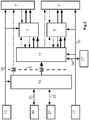
- the figure 3 shows a first embodiment corresponding to the architecture of the figure 2 .
- the arrows 31 and 33 respectively connect the first 15 and the second 17 feeds to the elements which they feed.
- the first power supply 15 feeds the control unit 13, the processing unit 11, the elements (5, 7) of the high side HS while the second power supply 17 feeds the elements (5 ', 7') of the low side LS .
- the control unit 13 is connected on the one hand to processing elements 30 of the vehicle, for example via a serial communication bus (also called “controller area network (CAN)” in English) 35 and on the other hand to sensors 27 of the vehicle or of the inverter 1 via a connection 32.
- CAN controller area network
- the control signals are represented by solid arrows and correspond to the modulation signals for the arrows 37 and to the clock signals for the arrows 39.
- the dotted arrows represent control signals and are of three types: arrows 41 in regular dotted lines correspond to error signals or fault signals, arrows 43 with a two-dot pattern and a line which correspond to monitoring signals (or "watchdog" signals in English) and the arrows 45 with a two-point and three-line pattern which correspond to the permission signals (or “enable” signals in English).
- the error signals 41 are sent when an anomaly is detected by an element while the monitoring signals 43 are sent continuously so that an absence of a monitoring signal or an abnormal signal can be interpreted as an error. dysfunction.
- the permission signals 45 make it possible to activate or deactivate an element, in particular to control an element so that it operates normally or in an alternative mode.
- the permission signals 45 are sent by the control unit 13 and the processing unit 11 to respectively the control units 7 'on the low side LS and the control units 7 on the high side HS so that when these permission signals 45 are at level 1, the driving units 7, 7 'drive the switches 3 and 3' according to the control signals received from the logic components 5 and 5 'and when the permission signals are at the level 0, the control units 7, 7 'are inhibited and no longer control the switches 3 and 3' which then remain open (the commands associated with level 0 and level 1 can obviously be reversed).
- the permission signal 45 takes a high impedance value. In the case of the present invention, this high impedance signal is interpreted as a signal at level 1, by example using a pull-up resistor or pull-up resistor at the control units 7, 7 '.
- this procedure aims to short-circuit, that is to say to close, the switches 3 on the high side HS of the inverter 1 while the other switches, on the low side LS , remain open, or to short-circuit the switches 3 'on the low side LS of the inverter 1 while the other switches, on the high side HS, remain open, so as to obtain a motor, and therefore a vehicle, coasting.
- the user can then use the mechanical brakes to immobilize the vehicle. This procedure helps prevent the vehicle from stopping suddenly.
- the various malfunctions, their detection mode and the commands implemented in the event of a malfunction being detected will now be described, for the configuration of the power supply and control circuit of the inverter of the unit. figure 3 from the summary table of the figure 4 .
- the first column of the table indicates the various malfunctions that can be encountered in inverter 1.
- the second column indicates the element of inverter 1 which detects the malfunction.
- the third column indicates the action generated in response to the malfunction, this action being initiated by the element that detected the malfunction indicated in the second column.
- the first type of malfunction corresponds to a malfunction of a switch 3, a control unit 7 or a logic component 5 on the high side HS.
- This malfunction is detected by the processing unit 11 via the comparators 21 or via the control signals, such as for example the error signals 41 returned by the first logic component 5 or the supervision signals 43 returned by the first logic component. 5 in the event of a malfunction of the first logic component 5.
- the detection of a malfunction can also correspond to the absence of reception of control signals. If the malfunction or failure causes a short-circuit of at least one of the switches 3 on the high side HS, which can be detected via the comparators 21, the processing unit 11 commands the closing of all the switches 3 of the high side HS and the opening of the switches 3 'on the low side LS.
- the processing unit 11 can indicate to the control unit 13 the malfunction via the error signals 41.
- the control unit 13 can then inhibit the control units 7 'on the low side LS via permission signals 45 to open switches 3 '. Otherwise, the processing unit 11 controls the closing of the switches 3 'on the low side LS via the second logic component 5'.
- the processing unit 11 inhibits the control units 7 on the high side HS via the permission signals 45.
- the first switches 3 are found in the open position while the second switches 3 'are found in short-circuit which results in the freewheeling of the vehicle.
- the second type of malfunction corresponds to a malfunction of a switch 3 ', a control unit 7' or a logic component 5 'on the low side LS of inverter 1. This malfunction is detected by the unit. processing 11 via the comparators 21 or via the control signals, such as for example the error signals 41 returned by the second logic component 5 'or the monitoring signals 43 returned by the second logic component 5' in the event of a malfunction of the second logic component 5 '. If the malfunction or failure leads to a short-circuit of at least one of the switches 3 'on the low side LS, which can be detected via the comparators 21, the processing unit 11 commands the closing of all the switches 3. 'on the low side LS and the opening of the switches 3 on the high side HS.
- the processing unit 11 can inhibit the control units 7 on the high side HS via the permission signals 45 to open the switches 3. Otherwise, the processing unit 11 controls the closing of the first switches 3 via the first logic component 5. The processing unit 11 indicates to the control unit 13 the malfunction via the error signals 41. The control unit command 13 then inhibits the pilot units 7 'on the low side LS via the permission signals 45. Thus, the first switches 3 are found in short-circuit while the second switches 3' are found open which causes the wheeling. free from the vehicle.
- the third type of malfunction corresponds to a malfunction of the control unit 13.
- This malfunction is detected by the processing unit 11 via the control signals sent by the control unit 13, that is to say either the error signals 41, or the monitoring signals 43 transmitted to the processing unit 11.
- the malfunction can also be detected by the control unit 13 itself by a self-diagnosis or by a component 25 dedicated to monitoring such as for example a basic chip (“System Basis Chip”).
- the processing unit 11 then controls the closing of the first switches 3 via the logic component 5 and controls the opening of the second switches 3 'via the second logic component 5'. If the control unit malfunctions 13 causes the permission signals 45 to go to 0, the second switches 3 'are also in the open position.
- the fourth type of malfunction corresponds to a malfunction of the processing unit 11. This malfunction is detected by the logic components 5 and 5 'thanks to the monitoring signals 43 and / or by the control unit 13 thanks to the monitoring signals. 43 or to error signals 41.
- the second logic component 5 'then controls the closing of the second switches 3' while the first logic component 5 controls the opening of the first switches 3.
- the first switches 3 are also found in the open position.
- the fifth type of malfunction corresponds to a malfunction of the first power supply 15. This malfunction is detected by the second logic component 5 'since the elements of the high side HS of the inverter 1, the control unit 11 and the control unit. treatment 13 are no longer supplied.
- the second logic component 5 'then controls the closing of the second switches 3'. As the control units 7 on the high side HS are not supplied with power, the first switches 3 are in the open position.
- the sixth type of malfunction corresponds to a malfunction of the second power supply 17. This malfunction is detected by the processing unit 11 via the comparators 21 or via the monitoring signals 43 returned (or not returned) by the second logic component 5 ′ . The processing unit 11 then controls the closing of the first switches 3 via the first logic component 5 and indicates the malfunction to the control unit 13 via the error signals 41.
- the configuration of the figure 3 enables the vehicle to be coasted when a malfunction appears on one of the components of the power supply and control circuit of inverter 1.
- the driver can immobilize the vehicle using the mechanical brake of the vehicle.
- the figure 5 shows a second configuration of the supply and control circuit of the inverter 1 in which the control unit 13 and the processing unit 11 are supplied by two different power sources.
- a barrier of potential 9 is placed between the control unit 13 and the processing unit 11.
- This potential barrier 9 eliminates the need for the potential barrier 9 located at the level of the control units 7, 7 '.
- a positioning of the potential barriers 9 as in the example illustrated in figure 3 is also possible.
- the signals exchanged between the control unit 13 and the processing unit 11 are the same as in the embodiment of the figure 3 but are grouped together in a serial peripheral interface type link so as to reduce the number of insulators necessary to achieve the potential barrier 9.
- the first power supply 15 feeds the control unit 13 and the components 5, 7 from the high side HS while the second power supply 17 feeds the processing unit 11 and the components 5 'and 7' from the low side LS.
- the control unit 13 is connected on the one hand to processing elements 30 of the vehicle, for example via a serial communication bus (also called “controller area network (CAN)” in English) 35 and on the other hand to sensors 27 of the vehicle or of the inverter 1 via a connection 32. Sensors 27 ′ can also be connected to the processing unit 11 via a connection 34.
- the control signals exchanged between the various elements of the supply circuit are the same as for the embodiment of the figure 3 .
- the first type of malfunction corresponds to a malfunction of a switch 3, a control unit 7 or a logic component 5 on the high side HS.
- This malfunction is detected by the processing unit 11 via the comparators 21 or via the control signals, such as for example the error signals 41 returned by the first logic component 5 or via the monitoring signals 43 returned by the first component logic 5 in the event of a malfunction of the first logic component 5.
- the processing unit 11 commands the closing of all the switches 3 of the high side HS and the opening of the switches 3 'on the low side LS.
- the processing unit 11 can inhibit the drive units 7 'of the low side LS via the permission signals 45 to open the switches 3'. Otherwise, the processing unit 11 controls the closing of the second switches 3 'via the second logic component 5' and indicates to the control unit 13 the malfunction via the error signals 41. The control unit 13 then inhibits the control units 7 on the high side HS via the permission signals 45 so as to put the first switches 3 in the open position. Thus, the first switches 3 are found in the open position while the second switches 3 'are found in a short circuit, which causes the vehicle to freewheel.
- the second type of malfunction corresponds to a malfunction of a switch 3 ', a control unit 7' or a logic component 5 'on the low side LS of inverter 1. This malfunction is detected by the unit. processing 11 via the comparators 21 or via the error signals 41 returned by the second logic component 5 'or via the control signals, such as for example the monitoring signals 43 returned by the second logic component 5' in the event of a malfunction of the second logic component 5 '. If the malfunction or failure leads to a short-circuit of at least one of the switches 3 'on the low side LS, which can be detected via the comparators 21, the processing unit 11 commands the closing of all the switches 3. 'on the low side LS and the opening of the switches 3 on the high side HS.
- the processing unit 11 can indicate to the control unit 13 the malfunction via the error signals 41.
- the control unit 13 can then inhibit the control units 7 on the high side HS via the signals permission 45 to open the switches 3. Otherwise, the processing unit 11 controls the closing of the first switches 3 via the first logic component 5.
- the processing unit 11 inhibits the control units 7 'on the low side LS via the permission signals 45.
- the first switches 3 are found in short circuit while the second switches 3 'are found open, which causes the vehicle to freewheel.
- the third type of malfunction corresponds to a malfunction of the control unit 13.
- This malfunction is detected by the processing unit 11 via the control signals sent by the control unit 13, that is to say either the error signals 41, that is to say the monitoring signals 43 transmitted to the processing unit 11.
- the malfunction can also be detected by the control unit 13 itself by a self-diagnosis or by a component 25 dedicated to monitoring such as a basic chip.
- the processing unit 11 then controls the opening of the first switches 3 via the first logic component 5 and the closing of the second switches 3 'via the second logic component 5'. If the malfunction of the control unit 13 causes the permission signals 45 to go to 0, the first switches 3 are also found to be open.
- the fourth type of malfunction is a malfunction of the unit. processing 11. This malfunction is detected by the logic components 5 and 5 'on the high side HS and on the low side LS thanks to the monitoring signals 43 as well as by the control unit 13 thanks to the monitoring signals 43 or the signals d. 'error 41.
- the second logic component 5' then controls the opening of the second switches 3 '.
- the first logic component 5 controls the closing of the first switches 3. If the malfunction of the processing unit 11 causes the permission signals 45 to go to 0, the second switches 3 'are also found open.
- the fifth type of malfunction corresponds to a malfunction of the first power supply 15. This malfunction is detected by the processing unit 11 via the comparators 21 or the error 41 or monitoring signals 43 originating from the first logic component 5 or from the 'control unit 13. The control unit 11 then controls the closing of the second switches 3' via the second logic component 5 ', the first switches 3 being open due to the absence of power supply to the components 3, 5, 7 on the high side HS.
- the sixth type of malfunction corresponds to a malfunction of the second power supply 17. This malfunction is detected by the first logic component 5 and / or by the control unit 13 via the absence of monitoring signals 43 from the control unit. processing 11. The first logic component 5 then controls the closing of the first switches 3, the second switches 3 'being open due to the absence of power supply to the components 3', 5 'and 7' on the low side LS.
- the configuration of the figure 5 also enables the vehicle to be coasted when a malfunction appears on one of the components of the power supply circuit of inverter 1.
- the driver can immobilize the vehicle by using the brake vehicle mechanics.
- the use of the logic components 5 and 5 'combined with the use of the two independent power sources 15 and 17 respectively for the high side HS and the low side LS of the inverter 1 therefore allow on the one hand a detection of 'a malfunction of an element of the inverter 1 and on the other hand to short-circuit the first switches 3 located on the high side HS or the second switches 3' located on the low side LS of the inverter 1.
- the Proposed embodiments also make it possible to put the other switches 3 or 3 'in the open position so as to obtain an electric motor with a first side of which the switches 3, 3 'are open and a second side whose switches 3', 3 are short-circuited and therefore a freewheeling vehicle which allows the driver to be able to manage the vehicle deceleration himself using the mechanical brake and therefore makes it possible to avoid sudden braking in the middle of a fast lane for example.
- Such a configuration of the inverter 1 makes it possible to ensure the safety of the users following a malfunction of one of the elements of the inverter 1 without this requiring numerous additional equipment which entails
Landscapes
- Engineering & Computer Science (AREA)
- Power Engineering (AREA)
- Life Sciences & Earth Sciences (AREA)
- Sustainable Development (AREA)
- Sustainable Energy (AREA)
- Transportation (AREA)
- Mechanical Engineering (AREA)
- Inverter Devices (AREA)
Claims (23)
- Wechselrichter (1) umfassend eine Mehrzahl von Zweigen (B1, B2, B3), die zwischen einem ersten Anschlusspunkt (C1) und einem zweiten Anschlusspunkt (C2) parallel geschaltet sind, wobei die Zweige (B1, B2, B3) einen ersten Schalter (3) in Reihe mit einem zweiten Schalter (3') umfassen, wobei die ersten Schalter (3) mit dem ersten Anschlusspunkt (C1) verbunden und auf einer Hochseite (HS) des Wechselrichters (1) angeordnet sind und die zweiten Schalter (3') mit dem zweiten Anschlusspunkt (C2) verbunden und auf einer Niedrigseite (LS) des Wechselrichters (1) angeordnet sind,
wobei die Hochseite (HS) des Wechselrichters (1) einen ersten Logikbaustein (5) umfasst, der für die Ansteuerung der ersten Schalter (3) vorgesehen ist, die Niedrigseite (LS) des Wechselrichters (1) einen zweiten Logikbaustein (5') umfasst, der für die Ansteuerung der zweiten Schalter (3') vorgesehen ist,
und dadurch gekennzeichnet, dass der erste Logikbaustein (5) und die ersten Schalter (3), die zur Hochseite (HS) gehören, von einer ersten Stromquelle (15) gespeist werden und der zweite Logikbaustein (5') und die zweiten Schalter (3'), die zur Niedrigseite (LS) gehören, von einer zweiten Stromquelle (17) gespeist werden, die von der ersten Stromquelle (15) unabhängig ist, wobei die erste Stromquelle (15) und die zweite Stromquelle (17) dazu ausgebildet sind, die ersten (3) beziehungsweise zweiten (3') Schalter unabhängig zu speisen, wodurch im Falle einer Störung der zweiten (17) beziehungsweise ersten (15) Stromquelle die ersten (3) beziehungsweise zweiten (3') Schalter gesteuert werden können. - Wechselrichter (1) nach Anspruch 1, ebenfalls umfassend eine Verarbeitungseinheit (11), die dazu ausgebildet ist, einerseits mit einer Steuereinheit (13) und andererseits mit dem ersten (5) und zweiten (5') Logikbaustein zu kommunizieren.
- Wechselrichter (1) nach Anspruch 2, wobei die Verarbeitungseinheit (11) dazu ausgebildet ist, eine Störung eines Elements (3, 3', 5, 5', 7, 7') auf der Hochseite (HS) oder Niedrigseite (LS) festzustellen.
- Wechselrichter (1) nach Anspruch 2 oder 3, ebenfalls umfassend eine Mehrzahl von Komparatoren (21), deren Eingänge jeweils mit den Mittelpunkten (R, S, T) der Zweige (B1, B2, B3) verbunden sind und deren Ausgänge mit der Verarbeitungseinheit (11) verbunden sind, wobei die Komparatoren (21) dazu ausgebildet sind, eine elektrische Größe ihres jeweiligen Mittelpunkts (R, S, T) mit einem Wert zu vergleichen, der von der Ausgestaltung der Schalter (3, 3') abhängig ist, wobei die Verarbeitungseinheit (11) dazu ausgebildet ist, eine Störung eines Elements (3, 3', 5, 5', 7, 7') auf der Hochseite (HS) oder Niedrigseite (LS) anhand einer Abweichung zwischen der elektrischen Größe und dem Wert festzustellen.
- Wechselrichter nach einem der Ansprüche 2 bis 4, wobei die Verarbeitungseinheit (11) dazu ausgebildet ist, eine Störung eines Elements (3, 5, 7) auf der Hochseite (HS) beziehungsweise eines Elements (3', 5', 7') auf der Niedrigseite (LS) anhand von Kontrollsignalen (41, 43) festzustellen, die vom Logikbaustein (5) auf der Hochseite (HS) beziehungsweise vom Logikbaustein (5') auf der Niedrigseite (LS) gesendet werden.
- Wechselrichter (1) nach einem der Ansprüche 2 bis 5, wobei die Logikbausteine (5, 5') auf der Hochseite (HS) und/oder der Niedrigseite (LS) dazu ausgebildet sind, eine Störung der Verarbeitungseinheit (11) anhand von Kontrollsignalen (41, 43) festzustellen, die von der Verarbeitungseinheit (11) gesendet werden.
- Wechselrichter (1) nach einem der Ansprüche 2 bis 6, wobei die Verarbeitungseinheit (11) dazu ausgebildet ist, die Kurzschließung der ersten (3) oder zweiten (3') Schalter in Abhängigkeit von einer Störung eines Elements (3, 3', 5, 5', 7, 7') auf der Hochseite (HS) oder Niedrigseite (LS) zu steuern.
- Wechselrichter (1) nach einem der Ansprüche 2 bis 7, wobei die Logikbausteine (5, 5') auf der Niedrigseite (LS) und der Hochseite (HS) dazu ausgebildet sind, die Kurzschließung der zweiten (3') beziehungsweise ersten (3) Schalter im Falle einer Störung der Verarbeitungseinheit (11) zu steuern.
- Wechselrichter (1) nach einem der Ansprüche 2 bis 8, wobei die Steuereinheit (13) dazu ausgebildet ist, eine Störung der Verarbeitungseinheit (11) anhand von Kontrollsignalen (41, 43) festzustellen, die von der Verarbeitungseinheit (11) gesendet werden, und/oder die Verarbeitungseinheit (11) dazu ausgebildet ist, eine Störung der Steuereinheit (13) anhand von Kontrollsignalen (41, 43) festzustellen, die von der Steuereinheit (13) gesendet werden.
- Wechselrichter (1) nach einem der Ansprüche 2 bis 9, wobei die Verarbeitungseinheit (11) oder die Steuereinheit (13) dazu ausgebildet sind, im Falle einer Störung die Kurzschließung der zweiten (3') oder ersten (3) Schalter zu steuern.
- Wechselrichter (1) nach einem der Ansprüche 2 bis 10, wobei die Steuereinheit (13) oder die Verarbeitungseinheit (11) dazu ausgebildet sind, die Kurzschließung der ersten (3) oder zweiten (3') Schalter mittels Erlaubnissignalen (45) zu steuern, die es gestatten, die ersten (3) oder zweiten (3') Schalter zu aktivieren oder zu deaktivieren.
- Wechselrichter (1) nach Anspruch 11, wobei die Steuereinheit (13) dazu ausgebildet ist, Erlaubnissignale (45) an die Hochseite (HS) zu senden, die es gestatten, die Schalter (3) auf der Hochseite (HS) zu aktivieren oder zu deaktivieren, und die Verarbeitungseinheit (11) dazu ausgebildet ist, Erlaubnissignale (45) an die Niedrigseite (LS) zu senden, die es gestatten, die Schalter (3') auf der Niedrigseite (LS) zu aktivieren oder zu deaktivieren; oder die Steuereinheit (13) dazu ausgebildet ist, Erlaubnissignale (45) an die Niedrigseite (LS) zu senden, die es gestatten, die Schalter (3') auf der Niedrigseite (LS) zu aktivieren oder zu deaktivieren, und die Verarbeitungseinheit (11) dazu ausgebildet ist, Erlaubnissignale (45) an die Hochseite (HS) zu senden, die es gestatten, die Schalter (3) auf der Hochseite (HS) zu aktivieren oder zu deaktivieren.
- Wechselrichter (1) nach einem der Ansprüche 2 bis 12, wobei die Verarbeitungseinheit (11) ein gesondertes Element der Steuereinheit (13) ist.
- Wechselrichter (1) nach einem der vorhergehenden Ansprüche, der dazu ausgebildet ist, einen Kraftfahrzeug-Elektromotor ausgehend von der ersten Stromquelle (15) oder der zweiten Stromquelle zu speisen.
- Wechselrichter nach einem der vorhergehenden Ansprüche, wobei die Hochseite (HS) erste Ansteuerungseinheiten (7) umfasst, die Niedrigseite (LS) zweite Ansteuerungseinheiten (7') umfasst, wobei die ersten und zweiten Schalter (3, 3') jeweils über die ersten (7) beziehungsweise zweiten (7') Ansteuerungseinheiten angesteuert werden.
- Wechselrichter (1) nach einem der vorhergehenden Ansprüche und den Ansprüchen 5 oder 9, wobei die Kontrollsignale Überwachungssignale (43) oder Fehlersignale (41) sind.
- Wechselrichter (1) nach einem der Ansprüche 2 bis 16, wobei die Verarbeitungseinheit (11) und die Steuereinheit (13) alle beide von einer selben Stromquelle gespeist werden, das heißt, dass entweder alle beide von der ersten Stromquelle (15) gespeist werden oder alle beide von der zweiten (17) Stromquelle gespeist werden.
- Wechselrichter (1) nach einem der Ansprüche 2 bis 16, wobei die Verarbeitungseinheit (11) und die Steuereinheit (13) von gesonderten Quellen gespeist werden, das heißt, dass entweder die Verarbeitungseinheit (11) von der ersten Stromquelle (15) gespeist wird und die Steuereinheit (13) von der zweiten Stromquelle (17) gespeist wird, oder die Verarbeitungseinheit (11) von der zweiten Stromquelle (17) gespeist wird und die Steuereinheit (13) von der ersten Stromquelle (15) gespeist wird.
- Verfahren zur Steuerung eines Wechselrichters (1) nach einem der Ansprüche 2 bis 18, wobei im Falle einer Störung der Verarbeitungseinheit (11) der erste Logikbaustein (5) beziehungsweise der zweite Logikbaustein (5') die Störung der Verarbeitungseinheit (11) anhand von Kontrollsignalen (43) feststellt, die von der Verarbeitungseinheit (11) gesendet werden, und die Kurzschließung der ersten (3) beziehungsweise zweiten (3') Schalter steuert.
- Verfahren zur Steuerung eines Wechselrichters (1) nach einem der Ansprüche 2 bis 18, wobei im Falle einer Störung eines Elements (3, 5, 7) auf der Hochseite (HS) oder eines Elements (3', 5', 7') auf der Niedrigseite (LS) die Verarbeitungseinheit (11) die Störung feststellt und die Kurzschließung der ersten Schalter (3) oder zweiten Schalter (3') in Abhängigkeit von der Art der Störung steuert.
- Verfahren zur Steuerung eines Wechselrichters (1) nach einem der Ansprüche 2 bis 18, wobei im Falle einer Störung der Steuereinheit (13) die Verarbeitungseinheit (11) die Störung der Steuereinheit (13) anhand von Kontrollsignalen (41, 43) feststellt, die von der Steuereinheit (13) gesendet werden, und die Kurzschließung der ersten (3) oder zweiten Schalter (3') steuert.
- Verfahren zur Steuerung eines Wechselrichters (1) nach einem der Ansprüche 2 bis 17, wobei die Verarbeitungseinheit (11) und die Steuereinheit (13) alle beide von der ersten (15) beziehungsweise zweiten (17) Stromquelle gespeist werden und wobei im Falle einer Störung der ersten (15) beziehungsweise zweiten (17) Stromquelle der zweite (5') beziehungsweise erste (5) Logikbaustein die Kurzschließung der zweiten (3') beziehungsweise ersten (3) Schalter steuert.
- Verfahren zur Steuerung eines Wechselrichters (1) nach einem der Ansprüche 2 bis 16 oder 18, wobei die Verarbeitungseinheit (11) von der ersten (15) beziehungsweise zweiten (17) Stromquelle gespeist wird und die Steuereinheit (13) von der zweiten (17) beziehungsweise ersten (15) Stromquelle gespeist wird; und wobei im Falle einer Störung der Stromquelle (15, 17), die die Steuereinheit (13) speist, die Verarbeitungseinheit (11) die Kurzschließung der Schalter (3', 3) steuert, die von ihrer Stromquelle (17, 15) gespeist werden; und im Falle einer Störung der Stromquelle (17, 15), die die Verarbeitungseinheit (11) speist, der Logikbaustein (5, 5'), der von der anderen Stromquelle (15, 17) gespeist wird, die Kurzschließung der Schalter (3, 3') steuert, die von dieser anderen Stromquelle (15, 17) gespeist werden.
Applications Claiming Priority (2)
| Application Number | Priority Date | Filing Date | Title |
|---|---|---|---|
| FR1461351A FR3029035B1 (fr) | 2014-11-24 | 2014-11-24 | Onduleur a securite renforcee |
| PCT/FR2015/053169 WO2016083714A1 (fr) | 2014-11-24 | 2015-11-23 | Onduleur a sécurité renforcée |
Publications (2)
| Publication Number | Publication Date |
|---|---|
| EP3224079A1 EP3224079A1 (de) | 2017-10-04 |
| EP3224079B1 true EP3224079B1 (de) | 2021-07-14 |
Family
ID=52692769
Family Applications (1)
| Application Number | Title | Priority Date | Filing Date |
|---|---|---|---|
| EP15820211.9A Active EP3224079B1 (de) | 2014-11-24 | 2015-11-23 | Wechselrichter mit verbesserter sicherheit |
Country Status (4)
| Country | Link |
|---|---|
| EP (1) | EP3224079B1 (de) |
| FR (1) | FR3029035B1 (de) |
| HU (1) | HUE055811T2 (de) |
| WO (1) | WO2016083714A1 (de) |
Families Citing this family (2)
| Publication number | Priority date | Publication date | Assignee | Title |
|---|---|---|---|---|
| FR3058591B1 (fr) | 2016-11-08 | 2019-02-01 | Valeo Equipements Electriques Moteur | Systeme de commande d'un convertisseur de tension comportant un dispositif de detection de defaillance |
| EP3993249A1 (de) | 2020-10-28 | 2022-05-04 | NXP USA, Inc. | Netzteil zur gewährleistung des sicheren verhaltens einer wechselrichteranwendung |
Citations (1)
| Publication number | Priority date | Publication date | Assignee | Title |
|---|---|---|---|---|
| US8410740B2 (en) * | 2010-08-06 | 2013-04-02 | Denso Corporation | Electric power conversion apparatus |
Family Cites Families (4)
| Publication number | Priority date | Publication date | Assignee | Title |
|---|---|---|---|---|
| TW328190B (en) * | 1994-06-14 | 1998-03-11 | Toshiba Co Ltd | Control device of brushless motor and method of fault detection and air conditioner |
| WO2009001468A1 (ja) * | 2007-06-28 | 2008-12-31 | Mitsubishi Electric Corporation | 電力変換装置 |
| US8502489B2 (en) * | 2008-10-15 | 2013-08-06 | Panasonic Corporation | Motor control device |
| JP5007754B2 (ja) * | 2010-05-14 | 2012-08-22 | 株式会社デンソー | 電力変換システムの放電制御装置 |
-
2014
- 2014-11-24 FR FR1461351A patent/FR3029035B1/fr active Active
-
2015
- 2015-11-23 EP EP15820211.9A patent/EP3224079B1/de active Active
- 2015-11-23 HU HUE15820211A patent/HUE055811T2/hu unknown
- 2015-11-23 WO PCT/FR2015/053169 patent/WO2016083714A1/fr not_active Ceased
Patent Citations (1)
| Publication number | Priority date | Publication date | Assignee | Title |
|---|---|---|---|---|
| US8410740B2 (en) * | 2010-08-06 | 2013-04-02 | Denso Corporation | Electric power conversion apparatus |
Also Published As
| Publication number | Publication date |
|---|---|
| FR3029035A1 (fr) | 2016-05-27 |
| WO2016083714A1 (fr) | 2016-06-02 |
| HUE055811T2 (hu) | 2021-12-28 |
| FR3029035B1 (fr) | 2018-01-12 |
| EP3224079A1 (de) | 2017-10-04 |
Similar Documents
| Publication | Publication Date | Title |
|---|---|---|
| CA2639392C (fr) | Dispositif securitaire de detection d'insuffisance de freinage electrique et de commutation sur un frein securitaire | |
| FR3025167B1 (fr) | Dispositif de commande de direction assistee electrique | |
| FR2778799A1 (fr) | Systeme de pilotage pour un moteur electrique a excitation permanente a au moins une phase | |
| US20110095601A1 (en) | Switch module for a power supply network and power supply network comprising at least one switch module | |
| EP3003859A1 (de) | Stromversorgungsvorrichtung für flugzeuge mit elektroantrieb | |
| FR2920611A1 (fr) | Dispositif de freinage electrique securitaire avec moteur a aimants permanents et regulation du couple de freinage. | |
| WO2016170262A1 (fr) | Regulateur de tension d'un alternateur de vehicule automobile, porte-balais regulateur et alternateurs correspondants | |
| WO2014001689A1 (fr) | Organe électrique à alimentation redondante et à moyens de protection anti-surintensité et diode couplés à ses prises de masse | |
| FR2987705A1 (fr) | Chaine d'alimentation d'une machine electrique synchrone, systeme de traction electrique comprenant une telle chaine, et procede de commande d'une telle chaine | |
| EP3224079B1 (de) | Wechselrichter mit verbesserter sicherheit | |
| FR3013004A1 (fr) | Commande securisee d'un rechauffeur electrique | |
| EP3221181B1 (de) | Verfahren zum wiederaufladen von energieakkumulationsmitteln, die an ein elektro- oder hybridfahrzeug montiert sind | |
| EP2766212A2 (de) | Sicheres verfahren zum abschneiden der stromversorgung eines elektromotors und entsprechende vorrichtung | |
| FR3117077A3 (fr) | Systeme de controle electronique pour vehicule automobile fonctionnant en temps reel, intelligent et sur de moteurs electriques de vehicules automobiles a propulsion electrique | |
| EP3900175B1 (de) | System zur steuerung eines spannungswandlers | |
| FR3047619A1 (fr) | Dispositif et procede de commutation symetrique de charge dans un pont en h | |
| WO2013014351A1 (fr) | Systeme de controle d'un redresseur de courant destine a charger une batterie d'un vehicule automobile electrique | |
| FR3126247A1 (fr) | Véhicule à contrôle de l’alimentation de son réseau de bord en présence d’un court-circuit | |
| FR3134253A1 (fr) | Procédé de pilotage d’un onduleur comprenant la sélection d’un mode de sécurité | |
| EP2882094B1 (de) | Verfahren zum Ableiten der in einem Stator eines Elektromotors gespeicherten Energie | |
| US20240268265A1 (en) | Braking of a motor during a battery disconnect | |
| FR3161321A1 (fr) | Systeme electrique comprenant une batterie de puissance adaptee pour activer un mode de court-circuit d’une machine electrique | |
| WO2024218097A1 (fr) | Module et methode de contrôle d'un convertisseur de tension | |
| FR3007699A1 (fr) | Procede de commande d'un groupe motopropulseur electrique optimisant la phase d'utilisation a faible vitesse | |
| JP2004338656A (ja) | 車両用操舵装置 |
Legal Events
| Date | Code | Title | Description |
|---|---|---|---|
| STAA | Information on the status of an ep patent application or granted ep patent |
Free format text: STATUS: THE INTERNATIONAL PUBLICATION HAS BEEN MADE |
|
| PUAI | Public reference made under article 153(3) epc to a published international application that has entered the european phase |
Free format text: ORIGINAL CODE: 0009012 |
|
| STAA | Information on the status of an ep patent application or granted ep patent |
Free format text: STATUS: REQUEST FOR EXAMINATION WAS MADE |
|
| 17P | Request for examination filed |
Effective date: 20170512 |
|
| AK | Designated contracting states |
Kind code of ref document: A1 Designated state(s): AL AT BE BG CH CY CZ DE DK EE ES FI FR GB GR HR HU IE IS IT LI LT LU LV MC MK MT NL NO PL PT RO RS SE SI SK SM TR |
|
| AX | Request for extension of the european patent |
Extension state: BA ME |
|
| DAV | Request for validation of the european patent (deleted) | ||
| DAX | Request for extension of the european patent (deleted) | ||
| STAA | Information on the status of an ep patent application or granted ep patent |
Free format text: STATUS: EXAMINATION IS IN PROGRESS |
|
| 17Q | First examination report despatched |
Effective date: 20190306 |
|
| GRAP | Despatch of communication of intention to grant a patent |
Free format text: ORIGINAL CODE: EPIDOSNIGR1 |
|
| STAA | Information on the status of an ep patent application or granted ep patent |
Free format text: STATUS: GRANT OF PATENT IS INTENDED |
|
| INTG | Intention to grant announced |
Effective date: 20210205 |
|
| GRAS | Grant fee paid |
Free format text: ORIGINAL CODE: EPIDOSNIGR3 |
|
| GRAA | (expected) grant |
Free format text: ORIGINAL CODE: 0009210 |
|
| STAA | Information on the status of an ep patent application or granted ep patent |
Free format text: STATUS: THE PATENT HAS BEEN GRANTED |
|
| AK | Designated contracting states |
Kind code of ref document: B1 Designated state(s): AL AT BE BG CH CY CZ DE DK EE ES FI FR GB GR HR HU IE IS IT LI LT LU LV MC MK MT NL NO PL PT RO RS SE SI SK SM TR |
|
| REG | Reference to a national code |
Ref country code: GB Ref legal event code: FG4D Free format text: NOT ENGLISH |
|
| REG | Reference to a national code |
Ref country code: DE Ref legal event code: R096 Ref document number: 602015071345 Country of ref document: DE |
|
| REG | Reference to a national code |
Ref country code: IE Ref legal event code: FG4D Free format text: LANGUAGE OF EP DOCUMENT: FRENCH |
|
| REG | Reference to a national code |
Ref country code: AT Ref legal event code: REF Ref document number: 1410376 Country of ref document: AT Kind code of ref document: T Effective date: 20210815 |
|
| REG | Reference to a national code |
Ref country code: LT Ref legal event code: MG9D |
|
| REG | Reference to a national code |
Ref country code: NL Ref legal event code: MP Effective date: 20210714 |
|
| REG | Reference to a national code |
Ref country code: AT Ref legal event code: MK05 Ref document number: 1410376 Country of ref document: AT Kind code of ref document: T Effective date: 20210714 |
|
| REG | Reference to a national code |
Ref country code: HU Ref legal event code: AG4A Ref document number: E055811 Country of ref document: HU |
|
| PG25 | Lapsed in a contracting state [announced via postgrant information from national office to epo] |
Ref country code: FI Free format text: LAPSE BECAUSE OF FAILURE TO SUBMIT A TRANSLATION OF THE DESCRIPTION OR TO PAY THE FEE WITHIN THE PRESCRIBED TIME-LIMIT Effective date: 20210714 Ref country code: ES Free format text: LAPSE BECAUSE OF FAILURE TO SUBMIT A TRANSLATION OF THE DESCRIPTION OR TO PAY THE FEE WITHIN THE PRESCRIBED TIME-LIMIT Effective date: 20210714 Ref country code: NL Free format text: LAPSE BECAUSE OF FAILURE TO SUBMIT A TRANSLATION OF THE DESCRIPTION OR TO PAY THE FEE WITHIN THE PRESCRIBED TIME-LIMIT Effective date: 20210714 Ref country code: NO Free format text: LAPSE BECAUSE OF FAILURE TO SUBMIT A TRANSLATION OF THE DESCRIPTION OR TO PAY THE FEE WITHIN THE PRESCRIBED TIME-LIMIT Effective date: 20211014 Ref country code: PT Free format text: LAPSE BECAUSE OF FAILURE TO SUBMIT A TRANSLATION OF THE DESCRIPTION OR TO PAY THE FEE WITHIN THE PRESCRIBED TIME-LIMIT Effective date: 20211115 Ref country code: LT Free format text: LAPSE BECAUSE OF FAILURE TO SUBMIT A TRANSLATION OF THE DESCRIPTION OR TO PAY THE FEE WITHIN THE PRESCRIBED TIME-LIMIT Effective date: 20210714 Ref country code: AT Free format text: LAPSE BECAUSE OF FAILURE TO SUBMIT A TRANSLATION OF THE DESCRIPTION OR TO PAY THE FEE WITHIN THE PRESCRIBED TIME-LIMIT Effective date: 20210714 Ref country code: BG Free format text: LAPSE BECAUSE OF FAILURE TO SUBMIT A TRANSLATION OF THE DESCRIPTION OR TO PAY THE FEE WITHIN THE PRESCRIBED TIME-LIMIT Effective date: 20211014 Ref country code: HR Free format text: LAPSE BECAUSE OF FAILURE TO SUBMIT A TRANSLATION OF THE DESCRIPTION OR TO PAY THE FEE WITHIN THE PRESCRIBED TIME-LIMIT Effective date: 20210714 Ref country code: RS Free format text: LAPSE BECAUSE OF FAILURE TO SUBMIT A TRANSLATION OF THE DESCRIPTION OR TO PAY THE FEE WITHIN THE PRESCRIBED TIME-LIMIT Effective date: 20210714 Ref country code: SE Free format text: LAPSE BECAUSE OF FAILURE TO SUBMIT A TRANSLATION OF THE DESCRIPTION OR TO PAY THE FEE WITHIN THE PRESCRIBED TIME-LIMIT Effective date: 20210714 |
|
| PG25 | Lapsed in a contracting state [announced via postgrant information from national office to epo] |
Ref country code: PL Free format text: LAPSE BECAUSE OF FAILURE TO SUBMIT A TRANSLATION OF THE DESCRIPTION OR TO PAY THE FEE WITHIN THE PRESCRIBED TIME-LIMIT Effective date: 20210714 Ref country code: LV Free format text: LAPSE BECAUSE OF FAILURE TO SUBMIT A TRANSLATION OF THE DESCRIPTION OR TO PAY THE FEE WITHIN THE PRESCRIBED TIME-LIMIT Effective date: 20210714 Ref country code: GR Free format text: LAPSE BECAUSE OF FAILURE TO SUBMIT A TRANSLATION OF THE DESCRIPTION OR TO PAY THE FEE WITHIN THE PRESCRIBED TIME-LIMIT Effective date: 20211015 |
|
| REG | Reference to a national code |
Ref country code: DE Ref legal event code: R097 Ref document number: 602015071345 Country of ref document: DE |
|
| PG25 | Lapsed in a contracting state [announced via postgrant information from national office to epo] |
Ref country code: DK Free format text: LAPSE BECAUSE OF FAILURE TO SUBMIT A TRANSLATION OF THE DESCRIPTION OR TO PAY THE FEE WITHIN THE PRESCRIBED TIME-LIMIT Effective date: 20210714 |
|
| PLBE | No opposition filed within time limit |
Free format text: ORIGINAL CODE: 0009261 |
|
| STAA | Information on the status of an ep patent application or granted ep patent |
Free format text: STATUS: NO OPPOSITION FILED WITHIN TIME LIMIT |
|
| PG25 | Lapsed in a contracting state [announced via postgrant information from national office to epo] |
Ref country code: SM Free format text: LAPSE BECAUSE OF FAILURE TO SUBMIT A TRANSLATION OF THE DESCRIPTION OR TO PAY THE FEE WITHIN THE PRESCRIBED TIME-LIMIT Effective date: 20210714 Ref country code: SK Free format text: LAPSE BECAUSE OF FAILURE TO SUBMIT A TRANSLATION OF THE DESCRIPTION OR TO PAY THE FEE WITHIN THE PRESCRIBED TIME-LIMIT Effective date: 20210714 Ref country code: RO Free format text: LAPSE BECAUSE OF FAILURE TO SUBMIT A TRANSLATION OF THE DESCRIPTION OR TO PAY THE FEE WITHIN THE PRESCRIBED TIME-LIMIT Effective date: 20210714 Ref country code: EE Free format text: LAPSE BECAUSE OF FAILURE TO SUBMIT A TRANSLATION OF THE DESCRIPTION OR TO PAY THE FEE WITHIN THE PRESCRIBED TIME-LIMIT Effective date: 20210714 Ref country code: CZ Free format text: LAPSE BECAUSE OF FAILURE TO SUBMIT A TRANSLATION OF THE DESCRIPTION OR TO PAY THE FEE WITHIN THE PRESCRIBED TIME-LIMIT Effective date: 20210714 Ref country code: AL Free format text: LAPSE BECAUSE OF FAILURE TO SUBMIT A TRANSLATION OF THE DESCRIPTION OR TO PAY THE FEE WITHIN THE PRESCRIBED TIME-LIMIT Effective date: 20210714 |
|
| 26N | No opposition filed |
Effective date: 20220419 |
|
| PG25 | Lapsed in a contracting state [announced via postgrant information from national office to epo] |
Ref country code: MC Free format text: LAPSE BECAUSE OF FAILURE TO SUBMIT A TRANSLATION OF THE DESCRIPTION OR TO PAY THE FEE WITHIN THE PRESCRIBED TIME-LIMIT Effective date: 20210714 |
|
| REG | Reference to a national code |
Ref country code: CH Ref legal event code: PL |
|
| PG25 | Lapsed in a contracting state [announced via postgrant information from national office to epo] |
Ref country code: LU Free format text: LAPSE BECAUSE OF NON-PAYMENT OF DUE FEES Effective date: 20211123 Ref country code: IT Free format text: LAPSE BECAUSE OF FAILURE TO SUBMIT A TRANSLATION OF THE DESCRIPTION OR TO PAY THE FEE WITHIN THE PRESCRIBED TIME-LIMIT Effective date: 20210714 Ref country code: BE Free format text: LAPSE BECAUSE OF NON-PAYMENT OF DUE FEES Effective date: 20211130 |
|
| REG | Reference to a national code |
Ref country code: BE Ref legal event code: MM Effective date: 20211130 |
|
| PG25 | Lapsed in a contracting state [announced via postgrant information from national office to epo] |
Ref country code: LI Free format text: LAPSE BECAUSE OF NON-PAYMENT OF DUE FEES Effective date: 20211130 Ref country code: CH Free format text: LAPSE BECAUSE OF NON-PAYMENT OF DUE FEES Effective date: 20211130 |
|
| PG25 | Lapsed in a contracting state [announced via postgrant information from national office to epo] |
Ref country code: IE Free format text: LAPSE BECAUSE OF NON-PAYMENT OF DUE FEES Effective date: 20211123 |
|
| PG25 | Lapsed in a contracting state [announced via postgrant information from national office to epo] |
Ref country code: CY Free format text: LAPSE BECAUSE OF FAILURE TO SUBMIT A TRANSLATION OF THE DESCRIPTION OR TO PAY THE FEE WITHIN THE PRESCRIBED TIME-LIMIT Effective date: 20210714 |
|
| P01 | Opt-out of the competence of the unified patent court (upc) registered |
Effective date: 20230528 |
|
| PG25 | Lapsed in a contracting state [announced via postgrant information from national office to epo] |
Ref country code: MK Free format text: LAPSE BECAUSE OF FAILURE TO SUBMIT A TRANSLATION OF THE DESCRIPTION OR TO PAY THE FEE WITHIN THE PRESCRIBED TIME-LIMIT Effective date: 20210714 |
|
| PG25 | Lapsed in a contracting state [announced via postgrant information from national office to epo] |
Ref country code: MT Free format text: LAPSE BECAUSE OF FAILURE TO SUBMIT A TRANSLATION OF THE DESCRIPTION OR TO PAY THE FEE WITHIN THE PRESCRIBED TIME-LIMIT Effective date: 20210714 |
|
| PG25 | Lapsed in a contracting state [announced via postgrant information from national office to epo] |
Ref country code: TR Free format text: LAPSE BECAUSE OF FAILURE TO SUBMIT A TRANSLATION OF THE DESCRIPTION OR TO PAY THE FEE WITHIN THE PRESCRIBED TIME-LIMIT Effective date: 20210714 |
|
| PGFP | Annual fee paid to national office [announced via postgrant information from national office to epo] |
Ref country code: HU Payment date: 20251021 Year of fee payment: 11 |
|
| PGFP | Annual fee paid to national office [announced via postgrant information from national office to epo] |
Ref country code: DE Payment date: 20251117 Year of fee payment: 11 |
|
| PGFP | Annual fee paid to national office [announced via postgrant information from national office to epo] |
Ref country code: GB Payment date: 20251126 Year of fee payment: 11 |
|
| PGFP | Annual fee paid to national office [announced via postgrant information from national office to epo] |
Ref country code: FR Payment date: 20251128 Year of fee payment: 11 |