EP3224945B1 - Système et procédé de réduction de claquement à l'arrêt - Google Patents
Système et procédé de réduction de claquement à l'arrêt Download PDFInfo
- Publication number
- EP3224945B1 EP3224945B1 EP15790517.5A EP15790517A EP3224945B1 EP 3224945 B1 EP3224945 B1 EP 3224945B1 EP 15790517 A EP15790517 A EP 15790517A EP 3224945 B1 EP3224945 B1 EP 3224945B1
- Authority
- EP
- European Patent Office
- Prior art keywords
- output
- close
- input
- signal
- power stage
- Prior art date
- Legal status (The legal status is an assumption and is not a legal conclusion. Google has not performed a legal analysis and makes no representation as to the accuracy of the status listed.)
- Active
Links
Images


Classifications
-
- H—ELECTRICITY
- H03—ELECTRONIC CIRCUITRY
- H03F—AMPLIFIERS
- H03F1/00—Details of amplifiers with only discharge tubes, only semiconductor devices or only unspecified devices as amplifying elements
- H03F1/30—Modifications of amplifiers to reduce influence of variations of temperature or supply voltage or other physical parameters
- H03F1/305—Modifications of amplifiers to reduce influence of variations of temperature or supply voltage or other physical parameters in case of switching on or off of a power supply
-
- H—ELECTRICITY
- H03—ELECTRONIC CIRCUITRY
- H03F—AMPLIFIERS
- H03F1/00—Details of amplifiers with only discharge tubes, only semiconductor devices or only unspecified devices as amplifying elements
- H03F1/02—Modifications of amplifiers to raise the efficiency, e.g. gliding Class A stages, use of an auxiliary oscillation
-
- H—ELECTRICITY
- H03—ELECTRONIC CIRCUITRY
- H03F—AMPLIFIERS
- H03F3/00—Amplifiers with only discharge tubes or only semiconductor devices as amplifying elements
- H03F3/181—Low-frequency amplifiers, e.g. audio preamplifiers
- H03F3/183—Low-frequency amplifiers, e.g. audio preamplifiers with semiconductor devices only
- H03F3/187—Low-frequency amplifiers, e.g. audio preamplifiers with semiconductor devices only in integrated circuits
-
- H—ELECTRICITY
- H03—ELECTRONIC CIRCUITRY
- H03F—AMPLIFIERS
- H03F3/00—Amplifiers with only discharge tubes or only semiconductor devices as amplifying elements
- H03F3/20—Power amplifiers, e.g. Class B amplifiers, Class C amplifiers
- H03F3/21—Power amplifiers, e.g. Class B amplifiers, Class C amplifiers with semiconductor devices only
- H03F3/217—Class D power amplifiers; Switching amplifiers
- H03F3/2173—Class D power amplifiers; Switching amplifiers of the bridge type
-
- H—ELECTRICITY
- H03—ELECTRONIC CIRCUITRY
- H03G—CONTROL OF AMPLIFICATION
- H03G3/00—Gain control in amplifiers or frequency changers
- H03G3/20—Automatic control
- H03G3/30—Automatic control in amplifiers having semiconductor devices
- H03G3/3005—Automatic control in amplifiers having semiconductor devices in amplifiers suitable for low-frequencies, e.g. audio amplifiers
- H03G3/301—Automatic control in amplifiers having semiconductor devices in amplifiers suitable for low-frequencies, e.g. audio amplifiers the gain being continuously variable
-
- H—ELECTRICITY
- H03—ELECTRONIC CIRCUITRY
- H03G—CONTROL OF AMPLIFICATION
- H03G3/00—Gain control in amplifiers or frequency changers
- H03G3/20—Automatic control
- H03G3/30—Automatic control in amplifiers having semiconductor devices
- H03G3/34—Muting amplifier when no signal is present
- H03G3/348—Muting in response to a mechanical action or to power supply variations, e.g. during tuning; Click removal circuits
-
- H—ELECTRICITY
- H03—ELECTRONIC CIRCUITRY
- H03F—AMPLIFIERS
- H03F2200/00—Indexing scheme relating to amplifiers
- H03F2200/03—Indexing scheme relating to amplifiers the amplifier being designed for audio applications
-
- H—ELECTRICITY
- H03—ELECTRONIC CIRCUITRY
- H03F—AMPLIFIERS
- H03F2200/00—Indexing scheme relating to amplifiers
- H03F2200/129—Indexing scheme relating to amplifiers there being a feedback over the complete amplifier
-
- H—ELECTRICITY
- H03—ELECTRONIC CIRCUITRY
- H03F—AMPLIFIERS
- H03F2200/00—Indexing scheme relating to amplifiers
- H03F2200/135—Indexing scheme relating to amplifiers there being a feedback over one or more internal stages in the global amplifier
-
- H—ELECTRICITY
- H03—ELECTRONIC CIRCUITRY
- H03F—AMPLIFIERS
- H03F2200/00—Indexing scheme relating to amplifiers
- H03F2200/144—Indexing scheme relating to amplifiers the feedback circuit of the amplifier stage comprising a passive resistor and passive capacitor
-
- H—ELECTRICITY
- H03—ELECTRONIC CIRCUITRY
- H03F—AMPLIFIERS
- H03F2200/00—Indexing scheme relating to amplifiers
- H03F2200/156—One or more switches are realised in the feedback circuit of the amplifier stage
-
- H—ELECTRICITY
- H03—ELECTRONIC CIRCUITRY
- H03F—AMPLIFIERS
- H03F2200/00—Indexing scheme relating to amplifiers
- H03F2200/258—Indexing scheme relating to amplifiers the input of the amplifier has voltage limiting means
-
- H—ELECTRICITY
- H03—ELECTRONIC CIRCUITRY
- H03F—AMPLIFIERS
- H03F2200/00—Indexing scheme relating to amplifiers
- H03F2200/342—Pulse code modulation being used in an amplifying circuit
-
- H—ELECTRICITY
- H03—ELECTRONIC CIRCUITRY
- H03F—AMPLIFIERS
- H03F2200/00—Indexing scheme relating to amplifiers
- H03F2200/426—Indexing scheme relating to amplifiers the amplifier comprising circuitry for protection against overload
-
- H—ELECTRICITY
- H03—ELECTRONIC CIRCUITRY
- H03F—AMPLIFIERS
- H03F2200/00—Indexing scheme relating to amplifiers
- H03F2200/441—Protection of an amplifier being implemented by clamping means
-
- H—ELECTRICITY
- H03—ELECTRONIC CIRCUITRY
- H03F—AMPLIFIERS
- H03F2200/00—Indexing scheme relating to amplifiers
- H03F2200/444—Diode used as protection means in an amplifier, e.g. as a limiter or as a switch
-
- H—ELECTRICITY
- H03—ELECTRONIC CIRCUITRY
- H03F—AMPLIFIERS
- H03F2200/00—Indexing scheme relating to amplifiers
- H03F2200/66—Clipping circuitry being present in an amplifier, i.e. the shape of the signal being modified
-
- H—ELECTRICITY
- H03—ELECTRONIC CIRCUITRY
- H03F—AMPLIFIERS
- H03F2200/00—Indexing scheme relating to amplifiers
- H03F2200/78—A comparator being used in a controlling circuit of an amplifier
-
- H—ELECTRICITY
- H03—ELECTRONIC CIRCUITRY
- H03G—CONTROL OF AMPLIFICATION
- H03G2201/00—Indexing scheme relating to subclass H03G
- H03G2201/10—Gain control characterised by the type of controlled element
- H03G2201/106—Gain control characterised by the type of controlled element being attenuating element
Definitions
- This invention relates to a switching power conversion system such as DC-AC, DC-DC or AC-AC conversion systems or any combination of the above mentioned. More specifically, the invention relates to close-down pop elimination in an audio amplifier.
- the invention may advantageously be used for improved close down in any audio amplifier system, in particular high precision DC-AC power conversion systems such as high efficiency audio amplification.
- the close down pop elimination system (i.e. pop elimination in an audio amplification system) can be a central element of an audio power conversion system.
- PWM Pulse-width modulation
- PCM pulse-code-modulated signal
- the output signal of the modulator is fed to a power stage where it is amplified.
- a typical power converter includes a switching power conversion stage, a filter and an analogue control system.
- a general problem is the presence of an audible signal at the output of the system even though there is no input signal applied to the audio power conversion system.
- the signal at the output at close-down is called pop.
- a contributing source to the pop can be energy stored in the demodulation filter.
- Another contributing source of the close-down pop can be non-controllable conduction of the MOSFETs at close-down which depends on the timing of the power stage.
- WO 2008072212 describes a system with an added extra power stage.
- US 20060182266 describes a system with charging of a DC block capacitor. Not for minimize pop in other types of systems.
- US 8,232,678 discloses a switching power conversion system having an extra power stage for pop reduction.
- US 2009/102550 discloses a class D amplifier with first and second mute circuits for reducing startup and closedown pop noise.
- the second mute circuit is turned on, thereby fixing the voltage at the output terminal of the filter.
- the first mute circuit is set active and the operation of the amplifier is stopped without noise.
- CN 101018041 discloses an amplifier having a higher switch frequency at start and stop to reduce pop noise.
- Fig. 1 shows a block diagram of an embodiment of the invention which will be described in greater detail in the following.
- the system 1 in Fig.1 comprises a class D amplifier including an attenuator 101 and/or a clipper 101, a compensator 102, a comparator 103, a power stage 104, a demodulation filter 105, a sequence controller 107, a close down timing block 106 that can find a specific point in a PWM pulse, a first feedback filter 108a that can be changed to increase the switch frequency of the system 1, a second feedback filter 108b and a third feedback filter 108c.
- the comparator 103 and power stage 104 may be referred to as a combined block, named a switching power stage.
- the system 1 has an amplifier input 110 (e.g. an audio signal) and an amplifier output 111 which may be directed to e.g. a loud speaker.
- the sequence of close down may be as follows.
- the input signal should be as close to zero as possible, this is done by the attenuator 101 and/or clipper 101.
- the switch frequency is slowly increased by slowly removing a pole in the first feedback filter 108a, and thirdly, the power stage 104 is disabled at a certain time in the PWM pulse.
- the attenuator and clipper block 101 can be only an attenuator or only a clipper or both.
- FIG. 2 a schematic drawing of the first feedback filter (108a in Fig. 1 ) together with an operational amplifier 205 is illustrated.
- the feedback filter can have a transfer function that consists of a pole by two resistors 201, 203 and a capacitor 202, and one end is connected to the output 210 of the power stage and the other end is connected to a negative input of an inverting operational amplifier 205, which is placed inside the compensator block. By shorting one of the resistors 201 the pole is removed. In a self oscillating amplifier this can increase the switch frequency.
- the pole will be removed in ideal systems having ideal components, i.e. the switch not having any resistance when closed and the operational amplifier being ideal.
- the pole is more likely to be moved (e.g. due to the switch still having some resistance even when it is closed (conducting)).
- the resistor 201 which is to be shorted should be chosen to be considerably smaller than the other resistor 203.
- the resistor 201 can be shorted with a switch 204.
- the switch 204 can be closed slowly or fast depending on the demands in the close-down sequence.
- the close-down timing in that case may be provided in a similar manner as the close-down timing for the power stage, i.e. with a close-down timing circuit.
- a system may be designed where the same close-down timing circuit provides two close-down timings; one for the close-down of the power stage and one for the closing of the switch in the feedback filter.
- the system may comprise two close-down timing circuits, one for each purpose.
- a switch that is closed slowly may e.g. have a close-down time of above 5 ⁇ s, such as e.g. 100 ⁇ s.
- a switch that is closed fast may for example have a close-down time below 100 ns, such as e.g. 1 ns.
- switch is to be understood as a device having a transfer function that can be varied between 0 dB (i.e. no attenuation through the device) and substantially - ⁇ dB (i.e. a very high attenuation through the device) according to a given, desired function of time.
- it can also be interpreted as a device that can be varied between 0 ohm (very low resistance) and ⁇ ohm (very high resistance), according to a given, desired function of time.
- closing-down time of a switch is the time when the switch goes from an open state (i.e. very high attenuation or very high resistance) to a closed state (i.e. very low attenuation or very low resistance).
- Fig. 3 illustrates a PWM signal 306 at the output 310 of a power stage of a single ended system together with a schematic signal 311 showing the enabling/disabling of the power stage.
- the PWM signal 306 is either high 301 or low 302, and one period 303 of the PWM signal 306 consists of one part that is "high” (positive) 301 and one part that is “low” (negative) 302.
- the duty cycle of the PWM signal 306 is approximately 50 %, i.e. the width 301 of the "high” part of the PWM signal is approximately the same as the width 302 of the "low” part of the PWM signal.
- close ⁇ down timing close ⁇ down time period time
- the "close-down time" 305 is defined as the time from the beginning of a pulse/period, in this example being the beginning of a "high" part 301, to the close-down point 307, i.e. the point 307a in the period where the power stage is disabled.
- the close-down point can also be in a "high" part 301; this however depends on the intended system application.
- the skilled artisan readily understands that embodiments where the beginning and close-down point is within the same part of a pulse are within the scope of the invention. It is to be understood that the illustration merely serves to elucidate the concept and terminology.
- the beginning of a pulse/period can alternatively be chosen to be the beginning of a "low part" 302.
- the system can be implemented so that the close down timing is set by an I2C (inter-integrated circuit) interface. Then the amplifier assembly may be tested with different close-down timings and the one resulting in the least "pop" can be found and implemented for each device (i.e. each specific amplifier assembly) or for a design.
- I2C inter-integrated circuit
- FIG. 4 An exemplary embodiment of the close down timing block 106 from fig. 1 is shown in figure 4 and which will be discussed in greater detail in the following.
- Fig. 4 an example of a practical realization of finding a specific close down timing of a power stage within a PWM pulse is shown.
- Finding a specific timing of the close down may be done by a circuit which includes a clock divider 402 constructing half the clock of an input signal 401, a current source 411 charging a capacitor 403 (with a current i ) in the clock divided PWM high period, a current source 412 discharging the capacitor 403, with a current ( i*x ) that is a ratio of the charging current ( i ), in the clock divided PWM low period and a comparator 404 measuring zero voltage crossing(s).
- the rising edge detecting block 414 serves to provide a pulse with a short width when there is a rising edge at the clock divider 402 output.
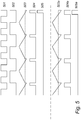
- the operation of the close-down timing circuit in Fig. 4 is further described with reference to Fig. 5 .
- Fig. 5 shows signals from the circuit in Fig. 4 , it should be noted that the signals illustrated in Fig. 5 are highly schematic and merely serve to further clarify an exemplary embodiment of the inventive concept; it should not be considered limiting to the invention.
- the first or top signal shown is the PWM input 501 to the close down timing circuit from the comparator 401.
- the clock divider output 502 producing an output that is half the frequency of the input signal (the PWM signal in 501).
- the capacitor voltage 503 is the voltage over the capacitor (403 in Fig. 4 ).
- the capacitor is charged by a first current i supplied by the current generator 411, and discharged by the current generator 412 by a second current i*x, which is a product of the first current and a predefined constant.
- the capacitor 403 is short circuited by the switch 413 which is controlled by a rising edge detection unit 414, which closes the switch 413 and thereby short circuits the capacitor 403, when a rising edge is detected in the clock divider output signal 502.
- the output 504 of the comparator (404 in Fig. 4 ) shows the rising edges that can be used for close down of the power stage, the timing of the rising edges shown in 504 depend on zero voltage crossings of the capacitor voltage 503.
- the close-down edge 505 is constructed by neglecting the first three rising edges and then using the fourth rising-edge as a close-down edge 505. This neglection of rising edges will be further explained in reference to Fig. 6 , more specifically in reference to section 607 in Fig. 6 .
- the bottom three signals in the figure 503a, 504a, 505a are the corresponding signals of 503, 504, 505 but with a larger predefined constant x, i.e. the discharging current is larger than in the previous example.
- Fig. 6 shows a detailed schematic of an exemplary embodiment of a close-down timing block in an integrated circuit application. Separate sections 601-611 have been marked in order to clarify the circuit in the figure and a brief description will be provided in the following.
- Section 601 in the close-down timing block includes input 621 for a reference current for the charging and discharging currents of the capacitor 622.
- the next section 602 comprises different current mirrors which can be used to choose between different close-down timings. This is done by changing the current that discharges a capacitor 622 in section 606 through the current mirror in section 610 and the switches 624, 625 in section 605.
- the different gate signals 602a-c in section 602 are used for setting different discharge currents of the capacitor 622 in section 606.
- section 603 is a current mirror used for the charging current of the capacitor 622. Further, section 604 has a clock divider that outputs 623 a signal that is half the frequency of its input signal.
- Section 605 contains switches that make a path for the discharge of the capacitor 622 in section 606. There are two switches 624, 625 in section 605, and the two switches 624, 625 are coupled in parallel for minimizing switching noise. When the two switches 624, 625 switch in or out the switching capacitance from one of the two switches 624, 625 is compensated by the other one of the two switches 624, 625.
- section 606 has a capacitor 622; however it also has a switch 626 that can short circuit the capacitor 622.
- a second capacitor 627 in section 606 which may be chosen to switch in parallel with the first capacitor 622, e.g. if one would want the system to work at a lower switch frequency. For example, if the switch frequency is not increased before close-down, the second capacitor 627 can be coupled in parallel with the first capacitor 622. This may for example be useful if one would like to avoid high frequency switching, e.g. in systems that have a big power stage where high frequency switching would result in high losses.
- section 607 comprises a comparator 630 that can measure when a voltage over the first (or primary) capacitor 622 is below a comparison/reference voltage 628 in order to generate a close-down timing signal 629.
- the close-down system can have some initialization time before the generated close-down timing of the power stage within the PWM-pulse is precise enough, so generally the first "rising edge(s)" outputted by the comparator 630 is(are) not used for the "close-down".
- a cascade of clock dividers can be used to neglect the first rising edge(s) and make sure the system is working properly before any rising edge is used as a "close-down edge”.
- section 608 includes circuitry for generating a short pulse in order to turn on the switch 626 in order to short circuit the capacitor 622, similarly to the operation of the rising edge detection block 414 in Fig. 4 .
- Section 609 contains a switch 631 that works at the same time as the switch 626 and compensates for the parasitic capacitances in switch 626 when it operates.
- Section 610 contains a current mirror which is used for the discharging current of the capacitor 622, and section 611 contains a buffer for the reference voltage 632 that the capacitor 622 is coupled to.
- the buffer in section 611 isolates the system from affecting the capacitor reference voltage 632 (if other circuits use this voltage) when the switch 626 is switched on and off, and furthermore the buffer keeps the output voltage of the buffer in 611 constant.
- the reference voltage 632 may be chosen to be higher than the other reference voltage 628 in section 607. This is in order to ensure that the comparator 630 is not mistakenly triggered when the switch 626 in section 606 is short circuiting the capacitor 622.
- Fig. 7 a detailed schematic of a compensator and "feedback switch" in an integrated circuit application is shown. This figure will follow a similar logic with marked sections 701-704 which will be described separately.
- Section 701 contains two operational amplifiers of the compensator, and section 702 contains an additional operational amplifier of the compensator that is coupled as an inverter.
- section 703 a switch 704 is shown which corresponds to the switch 204 shown in Fig. 2 .
- Section 704 includes another operational amplifier of the compensator, where the negative input of the operational amplifier in section 704 is coupled to the switch 703 and to a port.
- Fig. 8 illustrates a detailed schematic configuration for integrated circuit applications of a feedback switch.
- Fig. 8 has been divided in separate sections 801-806 in a corresponding fashion as in Figures 6 and 7 .
- Section 801 illustrates the bias distribution.
- the input reference bias current enters at port 811.
- a gate signal 812 can add an extra path to change the bias of the system.
- section 802 an "off circuit" for the switches 813 and 814 is shown. By delivering current into point 815 (source node) and pulling current out of point 816 (gate node), the voltage between the point 816 and 815 is lowered and the two switches 813, 814 are turned off.
- References 831a and 831b represent common signals between the different sections.
- section 803 contains an "on circuit" for the switches 813, 814 in section 805.
- the voltage between points 816 and 815 is increased and the switches 813, 814 are turned on. Since the current delivered to point 816 is very similar to the current pulled from point 815, only a small current (small magnitude) will be running into the points 820 and 821 in section 805.
- the current delivered/pulled to/from point 816 and point 815 together with the capacitance of the switches 813, 814 and the diode 817, and the circuit in section 806 determines how fast the switches 813, 814 are switching (i.e. changing from off to on and vice versa).
- An extra capacitor can be added between the gate node 816 and the source node 815 of the two switches 813, 814 in order to increase the switching time more.
- section 804 enabling circuits and bias current level control circuits are illustrated.
- the switches 813, 814 and the components associated with them are shown.
- the two transistors 813, 814 coupled in serial, are creating the switch function.
- the diode 817 is used to protect the voltage difference between point 816 and point 815 (i.e. between the gates and the sources of the switches 813, 814). By protect it is meant that the voltage cannot get too high or too low, which could lead to break-down of the two MOSFETs 813, 814.
- the resistance 818 here in the form of two resistors, is a very high value resistance in order to keep the midpoint 815 voltage value near the voltage value of point 821, when the switch/switches is/are off.
- Section 806 contains two transistors for limiting the different voltages between point 816 and 815 when the switch/switches is/are on or off, i.e. when the system is operating normally.
- Fig. 9 shows a simulation of the close-down sequence.
- the signal graphs 901-904 show voltages on the Y-axis and time on the X-axis.
- Signal 901 corresponds to the output of the power stage.
- 901a there is a PWM-signal
- 901b the PWM frequency (switch frequency) is slowly increased (by the removal of a pole in a feedback filter), and in the end 901c, after the power stage has been disabled, there is some residual ringing that is slowly decreasing.
- the signal 902 for controlling the switch for increasing the switch frequency is shown.
- the signal 902 is rising relatively slowly, in order to slowly turn the switch on and thereby slowly increase the switch frequency.
- a signal 903 for enabling or disabling the power stage is shown, it can be observed that the power stage is disabled by the signal in 903 at the beginning of 901c.
- the output signal 904 of the amplifier after it has been filtered through a demodulation filter (low pass filter) and an additional low pass filter for removing switching ripple so that the audio band signal is more visible, is shown.
- the close-down timing circuit can be constructed in various ways, e.g. the construction of the close down time point can be made with other types of circuits.
- a circuit that simply makes an RC delay from an edge of the PWM signal can also be used.
- a digital circuit can be used to make a given delay from an edge of the PWM signal to the close down time point.
- the clock frequency of the digital circuit should be above a certain frequency, e.g. for most applications this frequency could be at least more than 40MHz. It should be noted that the above-mentioned embodiments illustrate rather than limit the invention, and that those skilled in the art will be able to design many alternative embodiments without departing from the scope of the appended claims. In the claims, any reference signs placed between parentheses shall not be construed as limiting to the claim.
- the word “comprising” does not exclude the presence of other elements or steps than those listed in the claim.
- the word “a” or “an” preceding an element does not exclude the presence of a plurality of such elements.
Landscapes
- Engineering & Computer Science (AREA)
- Power Engineering (AREA)
- Multimedia (AREA)
- Microelectronics & Electronic Packaging (AREA)
- Amplifiers (AREA)
Claims (9)
- Système de réduction de claquement à la coupure pour un amplificateur de classe D auto-oscillant configuré pour recevoir un signal d'entrée sur une entrée d'amplificateur (110) et pour fournir un signal de sortie à une sortie d'amplificateur (111), ledit système de réduction de claquement à la coupure comprenant :un chemin direct couplé entre l'entrée d'amplificateur (110) et la sortie d'amplificateur (111), comprenant un atténuateur (101) ayant une entrée et une sortie, un compensateur (102) ayant une entrée et une sortie, un étage de puissance de commutation comprenant un comparateur (103) ayant une entrée et une sortie, et un étage de puissance (104) ayant une entrée et une sortie ;dans lequel l'entrée d'amplificateur (110) est couplée à l'entrée de l'atténuateur (101), la sortie de l'atténuateur (101) est couplée à l'entrée du compensateur (102), la sortie du compensateur (102) est couplée à l'entrée du comparateur (103) et la sortie du comparateur (103) est couplée à l'entrée de l'étage de puissance (104) ;un chemin de rétroaction couplé entre la sortie de l'étage de puissance (104) et un nœud de rétroaction dans le compensateur (102), ledit chemin de rétroaction comprenant un premier filtre de rétroaction (108a) ;un chemin de signal couplé entre la sortie du comparateur (103) et une unité de contrôle de séquence (107), ledit chemin de signal comprenant un circuit de synchronisation de coupure (106) configuré pour fournir un signal de synchronisation pour lequel le claquement audible est minimisé ;dans lequel ladite unité de contrôle de séquence (107) est configurée pour :éliminer d'abord le signal d'entrée en contrôlant l'atténuateur (101);augmenter ensuite la fréquence de commutation de l'étage de puissance de commutation en déplaçant un pôle dans une fonction de transfert du premier filtre de rétroaction (108a) ; etdésactiver finalement l'étage de puissance de commutation à un moment donné d'une impulsion de modulation de largeur d'impulsions PWM générée à la sortie du comparateur (103) de l'étage de puissance de commutation sur base dudit signal de synchronisation provenant dudit circuit de synchronisation de coupure (106).
- Système de réduction de claquement à la coupure selon la revendication 1, dans lequel ledit circuit de synchronisation de coupure (106) comprend :une première source de courant (411) configurée pour charger un condensateur (403) durant une période haute d'un signal PWM reçu de la sortie du comparateur avec un premier courant,une deuxième source de courant (412) configurée pour décharger le condensateur (403) avec un deuxième courant durant une période basse du signal PWM reçu de la sortie du comparateur, dans lequel le deuxième courant présente un ratio prédéfini par rapport au premier courant ; etun circuit (404) configuré pour fournir le signal de synchronisation en détectant le passage d'une tension seuil par une tension sur le condensateur.
- Système de réduction de claquement à la coupure selon la revendication 2, dans lequel ledit circuit de synchronisation de coupure (106) comprend en outre un diviseur d'horloge (402) connecté à la sortie du comparateur de manière à fournir un deuxième signal PWM de plus basse fréquence au circuit de synchronisation de coupure.
- Système de réduction de claquement à la coupure selon l'une quelconque des revendications précédentes, dans lequel le premier filtre de rétroaction comprend :deux résistances (201, 203) connectées en série ;un condensateur (202) connecté entre les deux résistances et la terre ;un commutateur (204) ponté sur l'une desdites deux résistances ;dans lequel ladite unité de contrôle de séquence est configurée pour fermer le commutateur de manière à déplacer le pôle dans la fonction de transfert dudit premier filtre de rétroaction, augmentant ainsi la fréquence de commutation de l'étage de puissance de commutation.
- Système de réduction de claquement à la coupure selon la revendication 4, dans lequel le commutateur (204) est ponté sur une première résistance (201) ayant la plus faible valeur de résistance parmi les deux résistances.
- Système de réduction de claquement à la coupure selon la revendication 4 ou 5, dans lequel ladite unité de contrôle de séquence est configurée pour contrôler ledit commutateur pour passer d'un état ouvert à un état fermé dans une période comprise entre 5 microsecondes et 200 microsecondes.
- Système de réduction de claquement à la coupure selon la revendication 4 ou 5, dans lequel ladite unité de contrôle de séquence est configurée pour contrôler ledit commutateur pour passer d'un état ouvert à un état fermé dans une période comprise entre 0,1 nanoseconde et 100 nanosecondes.
- Système de réduction de claquement à la coupure selon l'une quelconque des revendications précédentes, dans lequel le signal de synchronisation est dérivé du ratio de la durée écoulée depuis le démarrage d'une période PWM jusqu'au point de coupure dans ladite période PWM par la période totale d'un signal PWM.
- Procédé de réduction de claquement à la coupure dans un amplificateur de classe D auto-oscillant recevant un signal d'entrée à une entrée d'amplificateur (110) et fournissant un signal de sortie à une sortie d'amplificateur (111), le procédé comprenant :la fourniture d'un chemin direct couplé entre l'entrée d'amplificateur (110) et la sortie d'amplificateur (111), comprenant un atténuateur (101) ayant une entrée et une sortie, un compensateur (102) ayant une entrée et une sortie, un étage de puissance de commutation (103, 104) comprenant un comparateur (103) ayant une entrée et une sortie, et un étage de puissance (104) ayant une entrée et une sortie ;le couplage de l'entrée d'amplificateur (110) à l'entrée de l'atténuateur (101), de la sortie de l'atténuateur (101) à l'entrée du compensateur (102), de la sortie du compensateur (102) à l'entrée du comparateur (103), et de la sortie du comparateur (103) à l'entrée de l'étage de puissance (104) ;la fourniture d'un chemin de rétroaction couplé entre la sortie de l'étage de puissance (104) et un nœud de rétroaction dans le compensateur (102), ledit chemin de rétroaction comprenant un premier filtre de rétroaction (108a) ;la fourniture d'un chemin de signal couplé entre une sortie du comparateur (103) et une unité de contrôle de séquence (107), dans lequel ledit chemin de signal comprend un circuit de synchronisation de coupure (106) fournissant un signal de synchronisation pour lequel le claquement audible est minimisé ;dans lequel l'unité de contrôle de séquence (107) met en œuvre les étapes suivantes :élimination d'abord du signal d'entrée en contrôlant l'atténuateur (101);augmentation ensuite de la fréquence de commutation de l'étage de puissance de commutation (103, 104) en déplaçant un pôle d'une fonction de transfert du premier filtre de rétroaction (108a) ; etdésactivation finalement de l'étage de puissance de commutation (103, 104) à un moment donné d'une impulsion PWM générée à la sortie du comparateur (103) sur base dudit signal de synchronisation provenant dudit circuit de synchronisation de coupure (106).
Applications Claiming Priority (3)
| Application Number | Priority Date | Filing Date | Title |
|---|---|---|---|
| DKPA201400684 | 2014-11-26 | ||
| DKPA201500344 | 2015-06-17 | ||
| PCT/EP2015/075433 WO2016083081A1 (fr) | 2014-11-26 | 2015-11-02 | Système et procédé de réduction de claquement à l'arrêt |
Publications (2)
| Publication Number | Publication Date |
|---|---|
| EP3224945A1 EP3224945A1 (fr) | 2017-10-04 |
| EP3224945B1 true EP3224945B1 (fr) | 2020-11-25 |
Family
ID=54427736
Family Applications (1)
| Application Number | Title | Priority Date | Filing Date |
|---|---|---|---|
| EP15790517.5A Active EP3224945B1 (fr) | 2014-11-26 | 2015-11-02 | Système et procédé de réduction de claquement à l'arrêt |
Country Status (3)
| Country | Link |
|---|---|
| US (1) | US9991852B2 (fr) |
| EP (1) | EP3224945B1 (fr) |
| WO (1) | WO2016083081A1 (fr) |
Families Citing this family (2)
| Publication number | Priority date | Publication date | Assignee | Title |
|---|---|---|---|---|
| US10164576B2 (en) * | 2017-04-28 | 2018-12-25 | Cirrus Logic, Inc. | Amplifier offset cancellation using amplifier supply voltage |
| CN116631423A (zh) * | 2023-05-31 | 2023-08-22 | 北京探境科技有限公司 | 音频信号处理方法、装置、存储介质及电子设备 |
Family Cites Families (6)
| Publication number | Priority date | Publication date | Assignee | Title |
|---|---|---|---|---|
| US7492217B2 (en) * | 2004-11-12 | 2009-02-17 | Texas Instruments Incorporated | On-the-fly introduction of inter-channel delay in a pulse-width-modulation amplifier |
| JPWO2006132202A1 (ja) | 2005-06-10 | 2009-01-08 | ローム株式会社 | オーディオ信号増幅回路およびそれを用いた電子機器 |
| US8232678B2 (en) * | 2006-12-15 | 2012-07-31 | Bang & Olufsen Icepower A/S | Extra power stage added for pop elimination |
| CN100471044C (zh) * | 2007-03-08 | 2009-03-18 | 埃派克森微电子(上海)有限公司 | 抑制d类功率放大器pop音的频率切换电路及其方法 |
| TWI508430B (zh) * | 2012-08-30 | 2015-11-11 | Anpec Electronics Corp | 具有防爆音功能之單端輸出d類放大器 |
| KR101906817B1 (ko) * | 2014-10-24 | 2018-10-11 | 씨러스 로직 인코포레이티드 | 팝 노이즈를 최소화하거나 또는 제거하기 위한 가변 램프 업/다운 이득을 갖는 증폭기 |
-
2015
- 2015-11-02 EP EP15790517.5A patent/EP3224945B1/fr active Active
- 2015-11-02 WO PCT/EP2015/075433 patent/WO2016083081A1/fr not_active Ceased
- 2015-11-02 US US15/528,934 patent/US9991852B2/en active Active
Non-Patent Citations (1)
| Title |
|---|
| None * |
Also Published As
| Publication number | Publication date |
|---|---|
| US9991852B2 (en) | 2018-06-05 |
| US20170317651A1 (en) | 2017-11-02 |
| WO2016083081A1 (fr) | 2016-06-02 |
| EP3224945A1 (fr) | 2017-10-04 |
Similar Documents
| Publication | Publication Date | Title |
|---|---|---|
| JP4691404B2 (ja) | スイッチング制御回路、自励型dc−dcコンバータ | |
| JP6356140B2 (ja) | スロープ補償モジュール | |
| US9577525B2 (en) | Adaptive dead time control | |
| US9712046B2 (en) | Dead-time optimization of DC-DC converters | |
| US7965151B2 (en) | Pulse width modulator with two-way integrator | |
| US20140015503A1 (en) | Boot-strap circuit and voltage converting device thereof | |
| CN111224627B (zh) | 用于g类应用的具有嵌入式降压控制器的音频放大器 | |
| US20140285258A1 (en) | Silent start class-d amplifier | |
| US9590574B1 (en) | Pulse-width modulated (PWM) audio power amplifier with output transition slope control | |
| US20150162829A1 (en) | Control Module of Constant On-Time Mode and Voltage Converting Device thereof | |
| KR102158074B1 (ko) | 개방-루프 전하 펌프 | |
| JP2016119700A (ja) | 半導体装置 | |
| US6822884B1 (en) | Pulse width modulated charge pump | |
| US7545207B2 (en) | Control circuit and method for a switching amplifier | |
| US9385694B2 (en) | Low-power programmable oscillator and ramp generator | |
| US10164531B2 (en) | Adaptive control method for generating non overlapping time in output devices | |
| JP4966338B2 (ja) | ピークホールド形検波回路 | |
| US7230481B2 (en) | System and method for reducing audible artifacts in an audio system | |
| EP3224945B1 (fr) | Système et procédé de réduction de claquement à l'arrêt | |
| JP3981612B2 (ja) | 三角波発生装置、パルス幅変調信号生成装置、及び外部同期/内部同期/非同期切替装置 | |
| US11888394B2 (en) | High-efficiency pulse width modulation for switching power converters | |
| US7986179B2 (en) | Circuit and method for reducing popping sound | |
| US9825600B2 (en) | Class D amplifier and electronic devices including the same | |
| US7388426B2 (en) | Control circuit and method for a switching amplifier | |
| US12445098B2 (en) | Switching amplifier circuitry |
Legal Events
| Date | Code | Title | Description |
|---|---|---|---|
| STAA | Information on the status of an ep patent application or granted ep patent |
Free format text: STATUS: THE INTERNATIONAL PUBLICATION HAS BEEN MADE |
|
| PUAI | Public reference made under article 153(3) epc to a published international application that has entered the european phase |
Free format text: ORIGINAL CODE: 0009012 |
|
| STAA | Information on the status of an ep patent application or granted ep patent |
Free format text: STATUS: REQUEST FOR EXAMINATION WAS MADE |
|
| 17P | Request for examination filed |
Effective date: 20170523 |
|
| AK | Designated contracting states |
Kind code of ref document: A1 Designated state(s): AL AT BE BG CH CY CZ DE DK EE ES FI FR GB GR HR HU IE IS IT LI LT LU LV MC MK MT NL NO PL PT RO RS SE SI SK SM TR |
|
| AX | Request for extension of the european patent |
Extension state: BA ME |
|
| DAV | Request for validation of the european patent (deleted) | ||
| DAX | Request for extension of the european patent (deleted) | ||
| STAA | Information on the status of an ep patent application or granted ep patent |
Free format text: STATUS: EXAMINATION IS IN PROGRESS |
|
| 17Q | First examination report despatched |
Effective date: 20190514 |
|
| GRAP | Despatch of communication of intention to grant a patent |
Free format text: ORIGINAL CODE: EPIDOSNIGR1 |
|
| STAA | Information on the status of an ep patent application or granted ep patent |
Free format text: STATUS: GRANT OF PATENT IS INTENDED |
|
| INTG | Intention to grant announced |
Effective date: 20200610 |
|
| GRAS | Grant fee paid |
Free format text: ORIGINAL CODE: EPIDOSNIGR3 |
|
| GRAA | (expected) grant |
Free format text: ORIGINAL CODE: 0009210 |
|
| STAA | Information on the status of an ep patent application or granted ep patent |
Free format text: STATUS: THE PATENT HAS BEEN GRANTED |
|
| AK | Designated contracting states |
Kind code of ref document: B1 Designated state(s): AL AT BE BG CH CY CZ DE DK EE ES FI FR GB GR HR HU IE IS IT LI LT LU LV MC MK MT NL NO PL PT RO RS SE SI SK SM TR |
|
| REG | Reference to a national code |
Ref country code: GB Ref legal event code: FG4D |
|
| REG | Reference to a national code |
Ref country code: CH Ref legal event code: EP |
|
| REG | Reference to a national code |
Ref country code: DE Ref legal event code: R096 Ref document number: 602015062605 Country of ref document: DE |
|
| REG | Reference to a national code |
Ref country code: AT Ref legal event code: REF Ref document number: 1339449 Country of ref document: AT Kind code of ref document: T Effective date: 20201215 |
|
| REG | Reference to a national code |
Ref country code: IE Ref legal event code: FG4D |
|
| REG | Reference to a national code |
Ref country code: AT Ref legal event code: MK05 Ref document number: 1339449 Country of ref document: AT Kind code of ref document: T Effective date: 20201125 |
|
| REG | Reference to a national code |
Ref country code: NL Ref legal event code: MP Effective date: 20201125 |
|
| PG25 | Lapsed in a contracting state [announced via postgrant information from national office to epo] |
Ref country code: NO Free format text: LAPSE BECAUSE OF FAILURE TO SUBMIT A TRANSLATION OF THE DESCRIPTION OR TO PAY THE FEE WITHIN THE PRESCRIBED TIME-LIMIT Effective date: 20210225 Ref country code: PT Free format text: LAPSE BECAUSE OF FAILURE TO SUBMIT A TRANSLATION OF THE DESCRIPTION OR TO PAY THE FEE WITHIN THE PRESCRIBED TIME-LIMIT Effective date: 20210325 Ref country code: RS Free format text: LAPSE BECAUSE OF FAILURE TO SUBMIT A TRANSLATION OF THE DESCRIPTION OR TO PAY THE FEE WITHIN THE PRESCRIBED TIME-LIMIT Effective date: 20201125 Ref country code: FI Free format text: LAPSE BECAUSE OF FAILURE TO SUBMIT A TRANSLATION OF THE DESCRIPTION OR TO PAY THE FEE WITHIN THE PRESCRIBED TIME-LIMIT Effective date: 20201125 Ref country code: GR Free format text: LAPSE BECAUSE OF FAILURE TO SUBMIT A TRANSLATION OF THE DESCRIPTION OR TO PAY THE FEE WITHIN THE PRESCRIBED TIME-LIMIT Effective date: 20210226 |
|
| PG25 | Lapsed in a contracting state [announced via postgrant information from national office to epo] |
Ref country code: AT Free format text: LAPSE BECAUSE OF FAILURE TO SUBMIT A TRANSLATION OF THE DESCRIPTION OR TO PAY THE FEE WITHIN THE PRESCRIBED TIME-LIMIT Effective date: 20201125 Ref country code: BG Free format text: LAPSE BECAUSE OF FAILURE TO SUBMIT A TRANSLATION OF THE DESCRIPTION OR TO PAY THE FEE WITHIN THE PRESCRIBED TIME-LIMIT Effective date: 20210225 Ref country code: PL Free format text: LAPSE BECAUSE OF FAILURE TO SUBMIT A TRANSLATION OF THE DESCRIPTION OR TO PAY THE FEE WITHIN THE PRESCRIBED TIME-LIMIT Effective date: 20201125 Ref country code: LV Free format text: LAPSE BECAUSE OF FAILURE TO SUBMIT A TRANSLATION OF THE DESCRIPTION OR TO PAY THE FEE WITHIN THE PRESCRIBED TIME-LIMIT Effective date: 20201125 Ref country code: SE Free format text: LAPSE BECAUSE OF FAILURE TO SUBMIT A TRANSLATION OF THE DESCRIPTION OR TO PAY THE FEE WITHIN THE PRESCRIBED TIME-LIMIT Effective date: 20201125 Ref country code: IS Free format text: LAPSE BECAUSE OF FAILURE TO SUBMIT A TRANSLATION OF THE DESCRIPTION OR TO PAY THE FEE WITHIN THE PRESCRIBED TIME-LIMIT Effective date: 20210325 |
|
| REG | Reference to a national code |
Ref country code: LT Ref legal event code: MG9D |
|
| PG25 | Lapsed in a contracting state [announced via postgrant information from national office to epo] |
Ref country code: HR Free format text: LAPSE BECAUSE OF FAILURE TO SUBMIT A TRANSLATION OF THE DESCRIPTION OR TO PAY THE FEE WITHIN THE PRESCRIBED TIME-LIMIT Effective date: 20201125 |
|
| PG25 | Lapsed in a contracting state [announced via postgrant information from national office to epo] |
Ref country code: CZ Free format text: LAPSE BECAUSE OF FAILURE TO SUBMIT A TRANSLATION OF THE DESCRIPTION OR TO PAY THE FEE WITHIN THE PRESCRIBED TIME-LIMIT Effective date: 20201125 Ref country code: EE Free format text: LAPSE BECAUSE OF FAILURE TO SUBMIT A TRANSLATION OF THE DESCRIPTION OR TO PAY THE FEE WITHIN THE PRESCRIBED TIME-LIMIT Effective date: 20201125 Ref country code: SM Free format text: LAPSE BECAUSE OF FAILURE TO SUBMIT A TRANSLATION OF THE DESCRIPTION OR TO PAY THE FEE WITHIN THE PRESCRIBED TIME-LIMIT Effective date: 20201125 Ref country code: LT Free format text: LAPSE BECAUSE OF FAILURE TO SUBMIT A TRANSLATION OF THE DESCRIPTION OR TO PAY THE FEE WITHIN THE PRESCRIBED TIME-LIMIT Effective date: 20201125 Ref country code: RO Free format text: LAPSE BECAUSE OF FAILURE TO SUBMIT A TRANSLATION OF THE DESCRIPTION OR TO PAY THE FEE WITHIN THE PRESCRIBED TIME-LIMIT Effective date: 20201125 Ref country code: SK Free format text: LAPSE BECAUSE OF FAILURE TO SUBMIT A TRANSLATION OF THE DESCRIPTION OR TO PAY THE FEE WITHIN THE PRESCRIBED TIME-LIMIT Effective date: 20201125 |
|
| REG | Reference to a national code |
Ref country code: DE Ref legal event code: R097 Ref document number: 602015062605 Country of ref document: DE |
|
| PG25 | Lapsed in a contracting state [announced via postgrant information from national office to epo] |
Ref country code: DK Free format text: LAPSE BECAUSE OF FAILURE TO SUBMIT A TRANSLATION OF THE DESCRIPTION OR TO PAY THE FEE WITHIN THE PRESCRIBED TIME-LIMIT Effective date: 20201125 |
|
| PLBE | No opposition filed within time limit |
Free format text: ORIGINAL CODE: 0009261 |
|
| STAA | Information on the status of an ep patent application or granted ep patent |
Free format text: STATUS: NO OPPOSITION FILED WITHIN TIME LIMIT |
|
| PG25 | Lapsed in a contracting state [announced via postgrant information from national office to epo] |
Ref country code: NL Free format text: LAPSE BECAUSE OF FAILURE TO SUBMIT A TRANSLATION OF THE DESCRIPTION OR TO PAY THE FEE WITHIN THE PRESCRIBED TIME-LIMIT Effective date: 20201125 Ref country code: AL Free format text: LAPSE BECAUSE OF FAILURE TO SUBMIT A TRANSLATION OF THE DESCRIPTION OR TO PAY THE FEE WITHIN THE PRESCRIBED TIME-LIMIT Effective date: 20201125 Ref country code: IT Free format text: LAPSE BECAUSE OF FAILURE TO SUBMIT A TRANSLATION OF THE DESCRIPTION OR TO PAY THE FEE WITHIN THE PRESCRIBED TIME-LIMIT Effective date: 20201125 |
|
| 26N | No opposition filed |
Effective date: 20210826 |
|
| PG25 | Lapsed in a contracting state [announced via postgrant information from national office to epo] |
Ref country code: SI Free format text: LAPSE BECAUSE OF FAILURE TO SUBMIT A TRANSLATION OF THE DESCRIPTION OR TO PAY THE FEE WITHIN THE PRESCRIBED TIME-LIMIT Effective date: 20201125 |
|
| PG25 | Lapsed in a contracting state [announced via postgrant information from national office to epo] |
Ref country code: ES Free format text: LAPSE BECAUSE OF FAILURE TO SUBMIT A TRANSLATION OF THE DESCRIPTION OR TO PAY THE FEE WITHIN THE PRESCRIBED TIME-LIMIT Effective date: 20201125 |
|
| PG25 | Lapsed in a contracting state [announced via postgrant information from national office to epo] |
Ref country code: IS Free format text: LAPSE BECAUSE OF FAILURE TO SUBMIT A TRANSLATION OF THE DESCRIPTION OR TO PAY THE FEE WITHIN THE PRESCRIBED TIME-LIMIT Effective date: 20210325 |
|
| PG25 | Lapsed in a contracting state [announced via postgrant information from national office to epo] |
Ref country code: MC Free format text: LAPSE BECAUSE OF FAILURE TO SUBMIT A TRANSLATION OF THE DESCRIPTION OR TO PAY THE FEE WITHIN THE PRESCRIBED TIME-LIMIT Effective date: 20201125 |
|
| REG | Reference to a national code |
Ref country code: CH Ref legal event code: PL |
|
| PG25 | Lapsed in a contracting state [announced via postgrant information from national office to epo] |
Ref country code: LU Free format text: LAPSE BECAUSE OF NON-PAYMENT OF DUE FEES Effective date: 20211102 Ref country code: BE Free format text: LAPSE BECAUSE OF NON-PAYMENT OF DUE FEES Effective date: 20211130 |
|
| REG | Reference to a national code |
Ref country code: BE Ref legal event code: MM Effective date: 20211130 |
|
| PG25 | Lapsed in a contracting state [announced via postgrant information from national office to epo] |
Ref country code: IE Free format text: LAPSE BECAUSE OF NON-PAYMENT OF DUE FEES Effective date: 20211102 |
|
| PG25 | Lapsed in a contracting state [announced via postgrant information from national office to epo] |
Ref country code: HU Free format text: LAPSE BECAUSE OF FAILURE TO SUBMIT A TRANSLATION OF THE DESCRIPTION OR TO PAY THE FEE WITHIN THE PRESCRIBED TIME-LIMIT; INVALID AB INITIO Effective date: 20151102 |
|
| P01 | Opt-out of the competence of the unified patent court (upc) registered |
Effective date: 20230523 |
|
| PG25 | Lapsed in a contracting state [announced via postgrant information from national office to epo] |
Ref country code: CY Free format text: LAPSE BECAUSE OF FAILURE TO SUBMIT A TRANSLATION OF THE DESCRIPTION OR TO PAY THE FEE WITHIN THE PRESCRIBED TIME-LIMIT Effective date: 20201125 |
|
| PG25 | Lapsed in a contracting state [announced via postgrant information from national office to epo] |
Ref country code: LI Free format text: LAPSE BECAUSE OF NON-PAYMENT OF DUE FEES Effective date: 20220701 Ref country code: CH Free format text: LAPSE BECAUSE OF NON-PAYMENT OF DUE FEES Effective date: 20220701 |
|
| PG25 | Lapsed in a contracting state [announced via postgrant information from national office to epo] |
Ref country code: MK Free format text: LAPSE BECAUSE OF FAILURE TO SUBMIT A TRANSLATION OF THE DESCRIPTION OR TO PAY THE FEE WITHIN THE PRESCRIBED TIME-LIMIT Effective date: 20201125 |
|
| PG25 | Lapsed in a contracting state [announced via postgrant information from national office to epo] |
Ref country code: TR Free format text: LAPSE BECAUSE OF FAILURE TO SUBMIT A TRANSLATION OF THE DESCRIPTION OR TO PAY THE FEE WITHIN THE PRESCRIBED TIME-LIMIT Effective date: 20201125 |
|
| PG25 | Lapsed in a contracting state [announced via postgrant information from national office to epo] |
Ref country code: MT Free format text: LAPSE BECAUSE OF FAILURE TO SUBMIT A TRANSLATION OF THE DESCRIPTION OR TO PAY THE FEE WITHIN THE PRESCRIBED TIME-LIMIT Effective date: 20201125 |
|
| PGFP | Annual fee paid to national office [announced via postgrant information from national office to epo] |
Ref country code: DE Payment date: 20251021 Year of fee payment: 11 |
|
| PGFP | Annual fee paid to national office [announced via postgrant information from national office to epo] |
Ref country code: GB Payment date: 20251114 Year of fee payment: 11 |
|
| PGFP | Annual fee paid to national office [announced via postgrant information from national office to epo] |
Ref country code: FR Payment date: 20251112 Year of fee payment: 11 |