EP3226061A2 - Kopfmontierte anzeigevorrichtung - Google Patents
Kopfmontierte anzeigevorrichtung Download PDFInfo
- Publication number
- EP3226061A2 EP3226061A2 EP17158320.6A EP17158320A EP3226061A2 EP 3226061 A2 EP3226061 A2 EP 3226061A2 EP 17158320 A EP17158320 A EP 17158320A EP 3226061 A2 EP3226061 A2 EP 3226061A2
- Authority
- EP
- European Patent Office
- Prior art keywords
- head
- display device
- mounted display
- scattering particles
- display panel
- Prior art date
- Legal status (The legal status is an assumption and is not a legal conclusion. Google has not performed a legal analysis and makes no representation as to the accuracy of the status listed.)
- Withdrawn
Links
- 239000002245 particle Substances 0.000 claims abstract description 104
- 230000003287 optical effect Effects 0.000 claims abstract description 37
- 239000010410 layer Substances 0.000 claims description 79
- 239000002335 surface treatment layer Substances 0.000 claims description 13
- 229910044991 metal oxide Inorganic materials 0.000 claims description 5
- 150000004706 metal oxides Chemical class 0.000 claims description 5
- 229920003229 poly(methyl methacrylate) Polymers 0.000 claims description 4
- 239000004926 polymethyl methacrylate Substances 0.000 claims description 4
- ZMZHRHTZJDBLEX-UHFFFAOYSA-N (2-phenylphenyl) prop-2-enoate Chemical class C=CC(=O)OC1=CC=CC=C1C1=CC=CC=C1 ZMZHRHTZJDBLEX-UHFFFAOYSA-N 0.000 claims description 3
- 229920000877 Melamine resin Polymers 0.000 claims description 3
- 239000004793 Polystyrene Substances 0.000 claims description 3
- VYPSYNLAJGMNEJ-UHFFFAOYSA-N Silicium dioxide Chemical compound O=[Si]=O VYPSYNLAJGMNEJ-UHFFFAOYSA-N 0.000 claims description 3
- 239000011324 bead Substances 0.000 claims description 3
- CQEYYJKEWSMYFG-UHFFFAOYSA-N butyl acrylate Chemical compound CCCCOC(=O)C=C CQEYYJKEWSMYFG-UHFFFAOYSA-N 0.000 claims description 3
- MHCLJIVVJQQNKQ-UHFFFAOYSA-N ethyl carbamate;2-methylprop-2-enoic acid Chemical compound CCOC(N)=O.CC(=C)C(O)=O MHCLJIVVJQQNKQ-UHFFFAOYSA-N 0.000 claims description 3
- JDSHMPZPIAZGSV-UHFFFAOYSA-N melamine Chemical compound NC1=NC(N)=NC(N)=N1 JDSHMPZPIAZGSV-UHFFFAOYSA-N 0.000 claims description 3
- 230000007935 neutral effect Effects 0.000 claims description 3
- 229920000747 poly(lactic acid) Polymers 0.000 claims description 3
- 229920002223 polystyrene Polymers 0.000 claims description 3
- 229910052814 silicon oxide Inorganic materials 0.000 claims description 3
- 239000010408 film Substances 0.000 description 32
- 239000000758 substrate Substances 0.000 description 13
- 238000005538 encapsulation Methods 0.000 description 10
- 210000003128 head Anatomy 0.000 description 10
- 238000002834 transmittance Methods 0.000 description 10
- 239000012790 adhesive layer Substances 0.000 description 9
- 239000000463 material Substances 0.000 description 8
- -1 region Substances 0.000 description 6
- 239000011347 resin Substances 0.000 description 4
- 229920005989 resin Polymers 0.000 description 4
- 239000010409 thin film Substances 0.000 description 4
- 238000000034 method Methods 0.000 description 3
- 230000001133 acceleration Effects 0.000 description 2
- 230000003190 augmentative effect Effects 0.000 description 2
- 239000011521 glass Substances 0.000 description 2
- 238000002347 injection Methods 0.000 description 2
- 239000007924 injection Substances 0.000 description 2
- 238000002789 length control Methods 0.000 description 2
- 239000011368 organic material Substances 0.000 description 2
- 238000005191 phase separation Methods 0.000 description 2
- 210000001747 pupil Anatomy 0.000 description 2
- 238000001228 spectrum Methods 0.000 description 2
- DRSFVGQMPYTGJY-GNSLJVCWSA-N Deprodone propionate Chemical compound C1CC2=CC(=O)C=C[C@]2(C)[C@@H]2[C@@H]1[C@@H]1CC[C@@](C(C)=O)(OC(=O)CC)[C@@]1(C)C[C@@H]2O DRSFVGQMPYTGJY-GNSLJVCWSA-N 0.000 description 1
- JOYRKODLDBILNP-UHFFFAOYSA-N Ethyl urethane Chemical compound CCOC(N)=O JOYRKODLDBILNP-UHFFFAOYSA-N 0.000 description 1
- 239000004698 Polyethylene Substances 0.000 description 1
- 239000004743 Polypropylene Substances 0.000 description 1
- GWEVSGVZZGPLCZ-UHFFFAOYSA-N Titan oxide Chemical compound O=[Ti]=O GWEVSGVZZGPLCZ-UHFFFAOYSA-N 0.000 description 1
- NIXOWILDQLNWCW-UHFFFAOYSA-N acrylic acid group Chemical group C(C=C)(=O)O NIXOWILDQLNWCW-UHFFFAOYSA-N 0.000 description 1
- 239000002313 adhesive film Substances 0.000 description 1
- 230000008901 benefit Effects 0.000 description 1
- 230000008859 change Effects 0.000 description 1
- 239000011248 coating agent Substances 0.000 description 1
- 238000000576 coating method Methods 0.000 description 1
- 230000007423 decrease Effects 0.000 description 1
- 229920001971 elastomer Polymers 0.000 description 1
- 230000004438 eyesight Effects 0.000 description 1
- 238000010097 foam moulding Methods 0.000 description 1
- 230000014509 gene expression Effects 0.000 description 1
- 230000005525 hole transport Effects 0.000 description 1
- 229910010272 inorganic material Inorganic materials 0.000 description 1
- 239000011147 inorganic material Substances 0.000 description 1
- 239000004973 liquid crystal related substance Substances 0.000 description 1
- 230000004048 modification Effects 0.000 description 1
- 238000012986 modification Methods 0.000 description 1
- TWNQGVIAIRXVLR-UHFFFAOYSA-N oxo(oxoalumanyloxy)alumane Chemical compound O=[Al]O[Al]=O TWNQGVIAIRXVLR-UHFFFAOYSA-N 0.000 description 1
- 230000005043 peripheral vision Effects 0.000 description 1
- 239000004033 plastic Substances 0.000 description 1
- 229920003023 plastic Polymers 0.000 description 1
- 229920000515 polycarbonate Polymers 0.000 description 1
- 239000004417 polycarbonate Substances 0.000 description 1
- 229920000573 polyethylene Polymers 0.000 description 1
- 239000002952 polymeric resin Substances 0.000 description 1
- 229920001155 polypropylene Polymers 0.000 description 1
- 229920002635 polyurethane Polymers 0.000 description 1
- 239000004814 polyurethane Substances 0.000 description 1
- 230000002265 prevention Effects 0.000 description 1
- 230000008569 process Effects 0.000 description 1
- 229910052594 sapphire Inorganic materials 0.000 description 1
- 239000010980 sapphire Substances 0.000 description 1
- 239000000565 sealant Substances 0.000 description 1
- 239000000243 solution Substances 0.000 description 1
- 229920003002 synthetic resin Polymers 0.000 description 1
- OGIDPMRJRNCKJF-UHFFFAOYSA-N titanium oxide Inorganic materials [Ti]=O OGIDPMRJRNCKJF-UHFFFAOYSA-N 0.000 description 1
Images


Classifications
-
- G—PHYSICS
- G02—OPTICS
- G02B—OPTICAL ELEMENTS, SYSTEMS OR APPARATUS
- G02B5/00—Optical elements other than lenses
- G02B5/02—Diffusing elements; Afocal elements
- G02B5/0205—Diffusing elements; Afocal elements characterised by the diffusing properties
- G02B5/0236—Diffusing elements; Afocal elements characterised by the diffusing properties the diffusion taking place within the volume of the element
- G02B5/0242—Diffusing elements; Afocal elements characterised by the diffusing properties the diffusion taking place within the volume of the element by means of dispersed particles
-
- G—PHYSICS
- G02—OPTICS
- G02B—OPTICAL ELEMENTS, SYSTEMS OR APPARATUS
- G02B1/00—Optical elements characterised by the material of which they are made; Optical coatings for optical elements
- G02B1/04—Optical elements characterised by the material of which they are made; Optical coatings for optical elements made of organic materials, e.g. plastics
-
- G—PHYSICS
- G02—OPTICS
- G02B—OPTICAL ELEMENTS, SYSTEMS OR APPARATUS
- G02B25/00—Eyepieces; Magnifying glasses
- G02B25/002—Magnifying glasses
-
- G—PHYSICS
- G02—OPTICS
- G02B—OPTICAL ELEMENTS, SYSTEMS OR APPARATUS
- G02B27/00—Optical systems or apparatus not provided for by any of the groups G02B1/00 - G02B26/00, G02B30/00
- G02B27/01—Head-up displays
- G02B27/017—Head mounted
- G02B27/0172—Head mounted characterised by optical features
-
- G—PHYSICS
- G02—OPTICS
- G02B—OPTICAL ELEMENTS, SYSTEMS OR APPARATUS
- G02B5/00—Optical elements other than lenses
- G02B5/02—Diffusing elements; Afocal elements
- G02B5/0205—Diffusing elements; Afocal elements characterised by the diffusing properties
- G02B5/021—Diffusing elements; Afocal elements characterised by the diffusing properties the diffusion taking place at the element's surface, e.g. by means of surface roughening or microprismatic structures
-
- G—PHYSICS
- G02—OPTICS
- G02B—OPTICAL ELEMENTS, SYSTEMS OR APPARATUS
- G02B5/00—Optical elements other than lenses
- G02B5/02—Diffusing elements; Afocal elements
- G02B5/0273—Diffusing elements; Afocal elements characterized by the use
- G02B5/0278—Diffusing elements; Afocal elements characterized by the use used in transmission
-
- G—PHYSICS
- G02—OPTICS
- G02B—OPTICAL ELEMENTS, SYSTEMS OR APPARATUS
- G02B5/00—Optical elements other than lenses
- G02B5/20—Filters
- G02B5/205—Neutral density filters
-
- H—ELECTRICITY
- H10—SEMICONDUCTOR DEVICES; ELECTRIC SOLID-STATE DEVICES NOT OTHERWISE PROVIDED FOR
- H10K—ORGANIC ELECTRIC SOLID-STATE DEVICES
- H10K59/00—Integrated devices, or assemblies of multiple devices, comprising at least one organic light-emitting element covered by group H10K50/00
- H10K59/80—Constructional details
- H10K59/875—Arrangements for extracting light from the devices
- H10K59/877—Arrangements for extracting light from the devices comprising scattering means
-
- G—PHYSICS
- G02—OPTICS
- G02B—OPTICAL ELEMENTS, SYSTEMS OR APPARATUS
- G02B27/00—Optical systems or apparatus not provided for by any of the groups G02B1/00 - G02B26/00, G02B30/00
- G02B27/01—Head-up displays
- G02B27/0101—Head-up displays characterised by optical features
- G02B2027/0118—Head-up displays characterised by optical features comprising devices for improving the contrast of the display / brillance control visibility
-
- H—ELECTRICITY
- H10—SEMICONDUCTOR DEVICES; ELECTRIC SOLID-STATE DEVICES NOT OTHERWISE PROVIDED FOR
- H10K—ORGANIC ELECTRIC SOLID-STATE DEVICES
- H10K50/00—Organic light-emitting devices
- H10K50/80—Constructional details
- H10K50/85—Arrangements for extracting light from the devices
- H10K50/854—Arrangements for extracting light from the devices comprising scattering means
Definitions
- Embodiments of the inventive concept provide a head-mounted display device including a display panel including a plurality of pixels for displaying an image, a filter on the display panel including a scattering layer for scattering the image to generate a scattered image, the scattering layer including a base having a first refractive index, and scattering particles mixed with the base and having a second refractive index that is greater than the first refractive index, and an optical system on the filter for magnifying the scattered image.
- the filter may further include a film on the scattering layer, wherein the film is a transparent film.
- first direction, the second direction and the third direction are not limited to three directions of a rectangular coordinate system, and may be interpreted in a broader sense.
- first direction, the second direction, and the third direction may be perpendicular to one another, or may represent different directions that are not perpendicular to one another.
- the term “substantially,” “about,” and similar terms are used as terms of approximation and not as terms of degree, and are intended to account for the inherent deviations in measured or calculated values that would be recognized by those of ordinary skill in the art. Further, the use of “may” when describing embodiments of the present invention refers to “one or more embodiments of the present invention.” As used herein, the terms “use,” “using,” and “used” may be considered synonymous with the terms “utilize,” “utilizing,” and “utilized,” respectively. Also, the term “exemplary” is intended to refer to an example or illustration.
- the display panel unit DU includes a display panel DP and a filter SF.
- the display panel DP generates an image corresponding to image data input thereto.
- the display panel DP may be, but is not limited to, an organic light emitting display panel, a liquid crystal display panel, a plasma display panel, an electrophoretic display panel, or an electrowetting display panel.
- the display panel DP will be described as an organic light emitting display panel, but the display panel DP should not be limited thereto.
- the circuit layer ML includes a plurality of signal lines and electronic devices, which are arranged on the display panel DP.
- the circuit layer ML includes gate lines, data lines, and thin film transistors respectively corresponding to pixels.
- the filter SF is attached to a surface of the display panel DP on which an image is displayed.
- the filter SF includes a film OF and an adhesive layer AL.
- the adhesive layer AL is between the film OF and the display panel DP to attach the film OF to the display panel DP.
- the filter SF is located on the encapsulation layer ECL.
- the display panel DP is a rear surface light emitting type organic light emitting display panel, and the filter SF may be attached to the base substrate BS.
- a non-pixel area GA is an area between respective ones of the first, second, and third pixels PX1, PX2, and PX3.
- the scattering particles CU1 have a thickness TK (e.g., a thickness TK in the first direction DR1) of about 40 micrometers to about 200 micrometers, although the thickness TK of the scattering particles CU1 should not be limited thereto or thereby.
- the thickness TK of the scattering particles CU1 may be controlled by, or determined by, a resolution of the display panel DP.
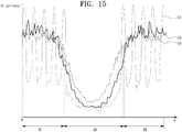
- the brightness variation in the area where the first image WT is displayed may be reduced, as represented by the second and third graphs G2 and G3. Accordingly, although the image is magnified by the optical system OL, the probability that the non-pixel area GA is perceived by the user may be reduced in the display panel unit DU including one of the filters SF1, SF2, SF3, SF4, SF5, and SF6 respectively shown in FIGS. 6, 7, 8 , 11 , 13, and 14 . Thus, the display quality of the head-mounted display device HMD may be improved.
Landscapes
- Physics & Mathematics (AREA)
- General Physics & Mathematics (AREA)
- Optics & Photonics (AREA)
- Chemical & Material Sciences (AREA)
- Dispersion Chemistry (AREA)
- Instrument Panels (AREA)
- Devices For Indicating Variable Information By Combining Individual Elements (AREA)
- Optical Elements Other Than Lenses (AREA)
- Electroluminescent Light Sources (AREA)
Applications Claiming Priority (1)
| Application Number | Priority Date | Filing Date | Title |
|---|---|---|---|
| KR1020160028477A KR20170105699A (ko) | 2016-03-09 | 2016-03-09 | 헤드 마운트 표시 장치 |
Publications (2)
| Publication Number | Publication Date |
|---|---|
| EP3226061A2 true EP3226061A2 (de) | 2017-10-04 |
| EP3226061A3 EP3226061A3 (de) | 2018-01-10 |
Family
ID=58227911
Family Applications (1)
| Application Number | Title | Priority Date | Filing Date |
|---|---|---|---|
| EP17158320.6A Withdrawn EP3226061A3 (de) | 2016-03-09 | 2017-02-28 | Kopfmontierte anzeigevorrichtung |
Country Status (6)
| Country | Link |
|---|---|
| US (1) | US20170261656A1 (de) |
| EP (1) | EP3226061A3 (de) |
| JP (1) | JP2017161903A (de) |
| KR (1) | KR20170105699A (de) |
| CN (1) | CN107179606A (de) |
| TW (1) | TW201800802A (de) |
Cited By (1)
| Publication number | Priority date | Publication date | Assignee | Title |
|---|---|---|---|---|
| TWI669537B (zh) * | 2018-01-24 | 2019-08-21 | 宏碁股份有限公司 | 顯示裝置 |
Families Citing this family (22)
| Publication number | Priority date | Publication date | Assignee | Title |
|---|---|---|---|---|
| KR102690986B1 (ko) * | 2016-03-23 | 2024-08-02 | 삼성디스플레이 주식회사 | 헤드 마운트 장치 및 표시 장치 |
| US10684543B2 (en) * | 2016-04-12 | 2020-06-16 | Corning Incorporated | Smart window projection screen |
| WO2019026748A1 (ja) * | 2017-08-02 | 2019-02-07 | シャープ株式会社 | 表示装置及びヘッドマウントディスプレイ |
| KR102500505B1 (ko) * | 2017-09-20 | 2023-02-16 | 삼성디스플레이 주식회사 | 헤드 마운트 표시 장치 |
| TWI657261B (zh) * | 2018-02-14 | 2019-04-21 | 雙瑩科技股份有限公司 | 虛擬及擴增實境組合裝置 |
| US11635622B1 (en) * | 2018-12-07 | 2023-04-25 | Meta Platforms Technologies, Llc | Nanovided spacer materials and corresponding systems and methods |
| KR102698107B1 (ko) * | 2019-07-29 | 2024-08-26 | 삼성디스플레이 주식회사 | 표시 장치 및 이의 구동 방법 |
| KR102851629B1 (ko) * | 2019-09-17 | 2025-08-28 | 삼성디스플레이 주식회사 | 발광 표시 장치 |
| KR20210073685A (ko) | 2019-12-10 | 2021-06-21 | 삼성디스플레이 주식회사 | 디스플레이 장치 |
| US12256057B2 (en) | 2019-12-31 | 2025-03-18 | ResMed Asia Pte. Ltd. | Positioning, stabilising, and interfacing structures and system incorporating same |
| US11262589B2 (en) | 2020-03-27 | 2022-03-01 | ResMed Pty Ltd | Positioning and stabilising structure and system incorporating same |
| US11686948B2 (en) * | 2020-03-27 | 2023-06-27 | ResMed Pty Ltd | Positioning, stabilising, and interfacing structures and system incorporating same |
| US12564236B2 (en) | 2020-03-27 | 2026-03-03 | ResMed Pty Ltd | Positioning and stabilising structure and system incorporating same |
| US11169384B2 (en) * | 2020-03-27 | 2021-11-09 | ResMed Pty Ltd | Positioning, stabilising, and interfacing structures and system incorporating same |
| US11598967B2 (en) | 2020-03-27 | 2023-03-07 | ResMed Pty Ltd | Positioning and stabilising structure and system incorporating same |
| US12554140B2 (en) | 2020-03-27 | 2026-02-17 | ResMed Pty Ltd | Positioning, stabilising, and interfacing structures and system incorporating same |
| US12178276B2 (en) | 2020-03-27 | 2024-12-31 | ResMed Pty Ltd | Positioning and stabilising structure and system incorporating same |
| CN113764599B (zh) * | 2020-06-04 | 2023-01-24 | 京东方科技集团股份有限公司 | 显示基板、其制作方法及显示面板 |
| KR102791632B1 (ko) * | 2020-12-31 | 2025-04-03 | 엘지디스플레이 주식회사 | 표시장치 |
| TWI790640B (zh) * | 2021-06-11 | 2023-01-21 | 宏碁股份有限公司 | 擴增實境顯示裝置與方法 |
| US20250035819A1 (en) * | 2022-01-10 | 2025-01-30 | Lg Electronics Inc. | Composite optical film and display device comprising same |
| CN118829322B (zh) * | 2024-06-28 | 2025-03-28 | 华为技术有限公司 | 显示模组和电子设备 |
Family Cites Families (19)
| Publication number | Priority date | Publication date | Assignee | Title |
|---|---|---|---|---|
| ATE185012T1 (de) * | 1991-07-03 | 1999-10-15 | Sun Microsystems Inc | Anzeigegeraet fuer virtuelle bilder |
| US5757544A (en) * | 1993-03-09 | 1998-05-26 | Olympus Optical Co., Ltd. | Image display apparatus |
| US6144491A (en) * | 1996-02-29 | 2000-11-07 | Dai Nippon Printing Co., Ltd. | Reflection-type projection screen |
| JP2005063838A (ja) * | 2003-08-13 | 2005-03-10 | Toshiba Matsushita Display Technology Co Ltd | 光学デバイス及び有機el表示装置 |
| CN201222102Y (zh) * | 2008-07-14 | 2009-04-15 | 宁波高新区激智科技有限公司 | 一种光学扩散薄膜及使用该光学扩散薄膜的液晶显示装置 |
| CN102299266A (zh) * | 2011-09-15 | 2011-12-28 | 四川虹视显示技术有限公司 | 有机电致发光器件的基板及制造方法 |
| WO2013061964A1 (ja) * | 2011-10-28 | 2013-05-02 | シャープ株式会社 | 表示装置 |
| US9625803B2 (en) * | 2012-02-27 | 2017-04-18 | Mitsubishi Electric Corporation | Screen, optical element, and display device |
| US9512976B2 (en) * | 2012-04-13 | 2016-12-06 | Sharp Kabushiki Kaisha | Light-emitting device, display device and illumination device |
| WO2014178230A1 (ja) * | 2013-04-30 | 2014-11-06 | リンテック株式会社 | ディスプレイ用光拡散フィルムおよびそれを用いた反射型表示装置 |
| US9019602B2 (en) * | 2013-05-30 | 2015-04-28 | City University Of Hong Kong | Scattering screen system, method of manufacture and application thereof |
| US9880328B2 (en) * | 2013-12-12 | 2018-01-30 | Corning Incorporated | Transparent diffusers for lightguides and luminaires |
| WO2015111351A1 (ja) * | 2014-01-27 | 2015-07-30 | コニカミノルタ株式会社 | 有機エレクトロルミネッセンス素子 |
| KR20150106016A (ko) * | 2014-03-10 | 2015-09-21 | 삼성디스플레이 주식회사 | 표시장치 |
| ES2788123T3 (es) * | 2014-06-02 | 2020-10-20 | Agc Inc | Estructura de proyección de video, procedimiento de proyección de video, y ventana de proyección de video |
| JPWO2016068087A1 (ja) * | 2014-10-27 | 2017-08-31 | 旭硝子株式会社 | 透過型透明スクリーン、映像表示システムおよび映像表示方法 |
| US20160178907A1 (en) * | 2014-12-17 | 2016-06-23 | Htc Corporation | Head-mounted electronic device and display thereof |
| WO2016104112A1 (ja) * | 2014-12-22 | 2016-06-30 | Jxエネルギー株式会社 | シート状透明成型体、それを備えた透明スクリーン、およびそれを備えた画像投影装置 |
| US10209412B2 (en) * | 2015-12-14 | 2019-02-19 | Facebook Technologies, Llc | Display with multilayer diffractive optical elements |
-
2016
- 2016-03-09 KR KR1020160028477A patent/KR20170105699A/ko not_active Withdrawn
-
2017
- 2017-01-06 US US15/400,696 patent/US20170261656A1/en not_active Abandoned
- 2017-02-28 EP EP17158320.6A patent/EP3226061A3/de not_active Withdrawn
- 2017-03-01 JP JP2017037975A patent/JP2017161903A/ja active Pending
- 2017-03-07 TW TW106107402A patent/TW201800802A/zh unknown
- 2017-03-08 CN CN201710133588.1A patent/CN107179606A/zh active Pending
Non-Patent Citations (1)
| Title |
|---|
| None |
Cited By (1)
| Publication number | Priority date | Publication date | Assignee | Title |
|---|---|---|---|---|
| TWI669537B (zh) * | 2018-01-24 | 2019-08-21 | 宏碁股份有限公司 | 顯示裝置 |
Also Published As
| Publication number | Publication date |
|---|---|
| KR20170105699A (ko) | 2017-09-20 |
| TW201800802A (zh) | 2018-01-01 |
| EP3226061A3 (de) | 2018-01-10 |
| US20170261656A1 (en) | 2017-09-14 |
| CN107179606A (zh) | 2017-09-19 |
| JP2017161903A (ja) | 2017-09-14 |
Similar Documents
| Publication | Publication Date | Title |
|---|---|---|
| EP3226061A2 (de) | Kopfmontierte anzeigevorrichtung | |
| CN103376551B (zh) | 小孔投射式近眼显示器 | |
| US10466479B2 (en) | Head-mounted display apparatus and optical system | |
| US10274741B2 (en) | Display for personal immersion apparatus | |
| US10983345B2 (en) | Head-mounted device and display device | |
| CN110574099B (zh) | 基于头部跟踪的场序跳视分离减少 | |
| CN106575044B (zh) | 显示装置和电子设备 | |
| KR20220040441A (ko) | 헤드 마운티드 디스플레이 장치 | |
| KR20170083690A (ko) | 헤드 마운트 장치 및 표시 장치 | |
| CN105652490A (zh) | 一种显示眼镜及其驱动方法 | |
| US11036321B2 (en) | Light control film and display apparatus including the same | |
| US10466393B2 (en) | Display device | |
| CN111754882A (zh) | 一种显示屏、vr眼镜 | |
| CN105849628A (zh) | 用于全息透视显示器的相位调制器 | |
| KR102743041B1 (ko) | 헤드 마운트 디스플레이장치 | |
| JP7262467B2 (ja) | 構造化光学表面及び光学イメージングシステム | |
| WO2017161599A1 (en) | Phase modulator for holographic see through display | |
| KR102765365B1 (ko) | 표시 장치, 헤드 마운트 표시 장치, 및 헤드 마운트용 표시 모듈 제조 방법 | |
| WO2022052769A1 (zh) | 光学成像系统及头戴显示装置 | |
| JP6805756B2 (ja) | 表示装置 | |
| CN112987330A (zh) | 集成式立体图像显示设备 | |
| US20240248308A1 (en) | Virtual image display device and head-mounted display apparatus | |
| US10012835B2 (en) | Image display device | |
| US20240353605A1 (en) | Light guiding plate, image display apparatus, and method for manufacturing light guiding plate | |
| US20240168694A1 (en) | Display device, and wearable device including the same |
Legal Events
| Date | Code | Title | Description |
|---|---|---|---|
| PUAI | Public reference made under article 153(3) epc to a published international application that has entered the european phase |
Free format text: ORIGINAL CODE: 0009012 |
|
| STAA | Information on the status of an ep patent application or granted ep patent |
Free format text: STATUS: THE APPLICATION HAS BEEN PUBLISHED |
|
| AK | Designated contracting states |
Kind code of ref document: A2 Designated state(s): AL AT BE BG CH CY CZ DE DK EE ES FI FR GB GR HR HU IE IS IT LI LT LU LV MC MK MT NL NO PL PT RO RS SE SI SK SM TR |
|
| AX | Request for extension of the european patent |
Extension state: BA ME |
|
| PUAL | Search report despatched |
Free format text: ORIGINAL CODE: 0009013 |
|
| AK | Designated contracting states |
Kind code of ref document: A3 Designated state(s): AL AT BE BG CH CY CZ DE DK EE ES FI FR GB GR HR HU IE IS IT LI LT LU LV MC MK MT NL NO PL PT RO RS SE SI SK SM TR |
|
| AX | Request for extension of the european patent |
Extension state: BA ME |
|
| RIC1 | Information provided on ipc code assigned before grant |
Ipc: G02B 5/02 20060101ALN20171205BHEP Ipc: G02B 27/01 20060101AFI20171205BHEP Ipc: H01L 51/52 20060101ALN20171205BHEP Ipc: G02B 5/20 20060101ALN20171205BHEP |
|
| STAA | Information on the status of an ep patent application or granted ep patent |
Free format text: STATUS: REQUEST FOR EXAMINATION WAS MADE |
|
| 17P | Request for examination filed |
Effective date: 20180705 |
|
| RBV | Designated contracting states (corrected) |
Designated state(s): AL AT BE BG CH CY CZ DE DK EE ES FI FR GB GR HR HU IE IS IT LI LT LU LV MC MK MT NL NO PL PT RO RS SE SI SK SM TR |
|
| STAA | Information on the status of an ep patent application or granted ep patent |
Free format text: STATUS: THE APPLICATION HAS BEEN WITHDRAWN |
|
| 18W | Application withdrawn |
Effective date: 20200205 |