EP3226071A1 - Substrat d'affichage, panneau d'affichage, son procédé de fabrication et dispositif d'affichage - Google Patents
Substrat d'affichage, panneau d'affichage, son procédé de fabrication et dispositif d'affichage Download PDFInfo
- Publication number
- EP3226071A1 EP3226071A1 EP15766038.2A EP15766038A EP3226071A1 EP 3226071 A1 EP3226071 A1 EP 3226071A1 EP 15766038 A EP15766038 A EP 15766038A EP 3226071 A1 EP3226071 A1 EP 3226071A1
- Authority
- EP
- European Patent Office
- Prior art keywords
- intermediate layer
- substrate
- transparent base
- base substrate
- light
- Prior art date
- Legal status (The legal status is an assumption and is not a legal conclusion. Google has not performed a legal analysis and makes no representation as to the accuracy of the status listed.)
- Granted
Links
- 239000000758 substrate Substances 0.000 title claims abstract description 211
- 238000000034 method Methods 0.000 title claims abstract description 75
- 230000003287 optical effect Effects 0.000 claims abstract description 76
- 238000004519 manufacturing process Methods 0.000 claims abstract description 59
- 239000000463 material Substances 0.000 claims abstract description 40
- OKTJSMMVPCPJKN-UHFFFAOYSA-N Carbon Chemical compound [C] OKTJSMMVPCPJKN-UHFFFAOYSA-N 0.000 claims description 25
- 239000004973 liquid crystal related substance Substances 0.000 claims description 25
- 239000004020 conductor Substances 0.000 claims description 10
- 239000011368 organic material Substances 0.000 claims description 8
- 238000001259 photo etching Methods 0.000 claims description 5
- 239000010410 layer Substances 0.000 description 168
- 239000010408 film Substances 0.000 description 41
- 210000004027 cell Anatomy 0.000 description 20
- 229920002120 photoresistant polymer Polymers 0.000 description 18
- 239000000243 solution Substances 0.000 description 7
- 238000002834 transmittance Methods 0.000 description 7
- 239000012044 organic layer Substances 0.000 description 6
- 238000005516 engineering process Methods 0.000 description 4
- 238000002347 injection Methods 0.000 description 4
- 239000007924 injection Substances 0.000 description 4
- 239000011159 matrix material Substances 0.000 description 4
- 238000005260 corrosion Methods 0.000 description 3
- 230000007797 corrosion Effects 0.000 description 3
- 239000011521 glass Substances 0.000 description 3
- 239000010453 quartz Substances 0.000 description 3
- 239000011347 resin Substances 0.000 description 3
- 229920005989 resin Polymers 0.000 description 3
- VYPSYNLAJGMNEJ-UHFFFAOYSA-N silicon dioxide Inorganic materials O=[Si]=O VYPSYNLAJGMNEJ-UHFFFAOYSA-N 0.000 description 3
- 230000005525 hole transport Effects 0.000 description 2
- 239000007788 liquid Substances 0.000 description 2
- 239000000565 sealant Substances 0.000 description 2
- 238000007789 sealing Methods 0.000 description 2
- 239000012780 transparent material Substances 0.000 description 2
- 239000011248 coating agent Substances 0.000 description 1
- 238000000576 coating method Methods 0.000 description 1
- 210000002858 crystal cell Anatomy 0.000 description 1
- AMGQUBHHOARCQH-UHFFFAOYSA-N indium;oxotin Chemical compound [In].[Sn]=O AMGQUBHHOARCQH-UHFFFAOYSA-N 0.000 description 1
- 238000001755 magnetron sputter deposition Methods 0.000 description 1
- 229910052751 metal Inorganic materials 0.000 description 1
- 239000002184 metal Substances 0.000 description 1
- 229910001092 metal group alloy Inorganic materials 0.000 description 1
- 150000002739 metals Chemical class 0.000 description 1
- 239000000049 pigment Substances 0.000 description 1
- 238000001179 sorption measurement Methods 0.000 description 1
- 239000000126 substance Substances 0.000 description 1
- 238000002207 thermal evaporation Methods 0.000 description 1
- 239000010409 thin film Substances 0.000 description 1
- YVTHLONGBIQYBO-UHFFFAOYSA-N zinc indium(3+) oxygen(2-) Chemical compound [O--].[Zn++].[In+3] YVTHLONGBIQYBO-UHFFFAOYSA-N 0.000 description 1
Images


Classifications
-
- G—PHYSICS
- G02—OPTICS
- G02F—OPTICAL DEVICES OR ARRANGEMENTS FOR THE CONTROL OF LIGHT BY MODIFICATION OF THE OPTICAL PROPERTIES OF THE MEDIA OF THE ELEMENTS INVOLVED THEREIN; NON-LINEAR OPTICS; FREQUENCY-CHANGING OF LIGHT; OPTICAL LOGIC ELEMENTS; OPTICAL ANALOGUE/DIGITAL CONVERTERS
- G02F1/00—Devices or arrangements for the control of the intensity, colour, phase, polarisation or direction of light arriving from an independent light source, e.g. switching, gating or modulating; Non-linear optics
- G02F1/01—Devices or arrangements for the control of the intensity, colour, phase, polarisation or direction of light arriving from an independent light source, e.g. switching, gating or modulating; Non-linear optics for the control of the intensity, phase, polarisation or colour
- G02F1/13—Devices or arrangements for the control of the intensity, colour, phase, polarisation or direction of light arriving from an independent light source, e.g. switching, gating or modulating; Non-linear optics for the control of the intensity, phase, polarisation or colour based on liquid crystals, e.g. single liquid crystal display cells
- G02F1/133—Constructional arrangements; Operation of liquid crystal cells; Circuit arrangements
- G02F1/1333—Constructional arrangements; Manufacturing methods
- G02F1/1335—Structural association of cells with optical devices, e.g. polarisers or reflectors
-
- G—PHYSICS
- G02—OPTICS
- G02B—OPTICAL ELEMENTS, SYSTEMS OR APPARATUS
- G02B5/00—Optical elements other than lenses
- G02B5/003—Light absorbing elements
-
- G—PHYSICS
- G02—OPTICS
- G02B—OPTICAL ELEMENTS, SYSTEMS OR APPARATUS
- G02B5/00—Optical elements other than lenses
- G02B5/18—Diffraction gratings
-
- G—PHYSICS
- G02—OPTICS
- G02F—OPTICAL DEVICES OR ARRANGEMENTS FOR THE CONTROL OF LIGHT BY MODIFICATION OF THE OPTICAL PROPERTIES OF THE MEDIA OF THE ELEMENTS INVOLVED THEREIN; NON-LINEAR OPTICS; FREQUENCY-CHANGING OF LIGHT; OPTICAL LOGIC ELEMENTS; OPTICAL ANALOGUE/DIGITAL CONVERTERS
- G02F1/00—Devices or arrangements for the control of the intensity, colour, phase, polarisation or direction of light arriving from an independent light source, e.g. switching, gating or modulating; Non-linear optics
- G02F1/01—Devices or arrangements for the control of the intensity, colour, phase, polarisation or direction of light arriving from an independent light source, e.g. switching, gating or modulating; Non-linear optics for the control of the intensity, phase, polarisation or colour
- G02F1/13—Devices or arrangements for the control of the intensity, colour, phase, polarisation or direction of light arriving from an independent light source, e.g. switching, gating or modulating; Non-linear optics for the control of the intensity, phase, polarisation or colour based on liquid crystals, e.g. single liquid crystal display cells
- G02F1/133—Constructional arrangements; Operation of liquid crystal cells; Circuit arrangements
- G02F1/1333—Constructional arrangements; Manufacturing methods
- G02F1/1335—Structural association of cells with optical devices, e.g. polarisers or reflectors
- G02F1/133509—Filters, e.g. light shielding masks
- G02F1/133512—Light shielding layers, e.g. black matrix
-
- G—PHYSICS
- G02—OPTICS
- G02F—OPTICAL DEVICES OR ARRANGEMENTS FOR THE CONTROL OF LIGHT BY MODIFICATION OF THE OPTICAL PROPERTIES OF THE MEDIA OF THE ELEMENTS INVOLVED THEREIN; NON-LINEAR OPTICS; FREQUENCY-CHANGING OF LIGHT; OPTICAL LOGIC ELEMENTS; OPTICAL ANALOGUE/DIGITAL CONVERTERS
- G02F1/00—Devices or arrangements for the control of the intensity, colour, phase, polarisation or direction of light arriving from an independent light source, e.g. switching, gating or modulating; Non-linear optics
- G02F1/01—Devices or arrangements for the control of the intensity, colour, phase, polarisation or direction of light arriving from an independent light source, e.g. switching, gating or modulating; Non-linear optics for the control of the intensity, phase, polarisation or colour
- G02F1/13—Devices or arrangements for the control of the intensity, colour, phase, polarisation or direction of light arriving from an independent light source, e.g. switching, gating or modulating; Non-linear optics for the control of the intensity, phase, polarisation or colour based on liquid crystals, e.g. single liquid crystal display cells
- G02F1/133—Constructional arrangements; Operation of liquid crystal cells; Circuit arrangements
- G02F1/1333—Constructional arrangements; Manufacturing methods
- G02F1/1335—Structural association of cells with optical devices, e.g. polarisers or reflectors
- G02F1/133509—Filters, e.g. light shielding masks
- G02F1/133514—Colour filters
-
- G—PHYSICS
- G02—OPTICS
- G02F—OPTICAL DEVICES OR ARRANGEMENTS FOR THE CONTROL OF LIGHT BY MODIFICATION OF THE OPTICAL PROPERTIES OF THE MEDIA OF THE ELEMENTS INVOLVED THEREIN; NON-LINEAR OPTICS; FREQUENCY-CHANGING OF LIGHT; OPTICAL LOGIC ELEMENTS; OPTICAL ANALOGUE/DIGITAL CONVERTERS
- G02F1/00—Devices or arrangements for the control of the intensity, colour, phase, polarisation or direction of light arriving from an independent light source, e.g. switching, gating or modulating; Non-linear optics
- G02F1/01—Devices or arrangements for the control of the intensity, colour, phase, polarisation or direction of light arriving from an independent light source, e.g. switching, gating or modulating; Non-linear optics for the control of the intensity, phase, polarisation or colour
- G02F1/13—Devices or arrangements for the control of the intensity, colour, phase, polarisation or direction of light arriving from an independent light source, e.g. switching, gating or modulating; Non-linear optics for the control of the intensity, phase, polarisation or colour based on liquid crystals, e.g. single liquid crystal display cells
- G02F1/133—Constructional arrangements; Operation of liquid crystal cells; Circuit arrangements
- G02F1/1333—Constructional arrangements; Manufacturing methods
- G02F1/1335—Structural association of cells with optical devices, e.g. polarisers or reflectors
- G02F1/133524—Light-guides, e.g. fibre-optic bundles, louvered or jalousie light-guides
-
- H—ELECTRICITY
- H10—SEMICONDUCTOR DEVICES; ELECTRIC SOLID-STATE DEVICES NOT OTHERWISE PROVIDED FOR
- H10K—ORGANIC ELECTRIC SOLID-STATE DEVICES
- H10K50/00—Organic light-emitting devices
- H10K50/80—Constructional details
- H10K50/85—Arrangements for extracting light from the devices
- H10K50/858—Arrangements for extracting light from the devices comprising refractive means, e.g. lenses
-
- H—ELECTRICITY
- H10—SEMICONDUCTOR DEVICES; ELECTRIC SOLID-STATE DEVICES NOT OTHERWISE PROVIDED FOR
- H10K—ORGANIC ELECTRIC SOLID-STATE DEVICES
- H10K50/00—Organic light-emitting devices
- H10K50/80—Constructional details
- H10K50/86—Arrangements for improving contrast, e.g. preventing reflection of ambient light
- H10K50/865—Arrangements for improving contrast, e.g. preventing reflection of ambient light comprising light absorbing layers, e.g. light-blocking layers
-
- H—ELECTRICITY
- H10—SEMICONDUCTOR DEVICES; ELECTRIC SOLID-STATE DEVICES NOT OTHERWISE PROVIDED FOR
- H10K—ORGANIC ELECTRIC SOLID-STATE DEVICES
- H10K59/00—Integrated devices, or assemblies of multiple devices, comprising at least one organic light-emitting element covered by group H10K50/00
- H10K59/80—Constructional details
- H10K59/8791—Arrangements for improving contrast, e.g. preventing reflection of ambient light
- H10K59/8792—Arrangements for improving contrast, e.g. preventing reflection of ambient light comprising light absorbing layers, e.g. black layers
-
- H—ELECTRICITY
- H10—SEMICONDUCTOR DEVICES; ELECTRIC SOLID-STATE DEVICES NOT OTHERWISE PROVIDED FOR
- H10K—ORGANIC ELECTRIC SOLID-STATE DEVICES
- H10K77/00—Constructional details of devices covered by this subclass and not covered by groups H10K10/80, H10K30/80, H10K50/80 or H10K59/80
- H10K77/10—Substrates, e.g. flexible substrates
-
- G—PHYSICS
- G02—OPTICS
- G02F—OPTICAL DEVICES OR ARRANGEMENTS FOR THE CONTROL OF LIGHT BY MODIFICATION OF THE OPTICAL PROPERTIES OF THE MEDIA OF THE ELEMENTS INVOLVED THEREIN; NON-LINEAR OPTICS; FREQUENCY-CHANGING OF LIGHT; OPTICAL LOGIC ELEMENTS; OPTICAL ANALOGUE/DIGITAL CONVERTERS
- G02F1/00—Devices or arrangements for the control of the intensity, colour, phase, polarisation or direction of light arriving from an independent light source, e.g. switching, gating or modulating; Non-linear optics
- G02F1/01—Devices or arrangements for the control of the intensity, colour, phase, polarisation or direction of light arriving from an independent light source, e.g. switching, gating or modulating; Non-linear optics for the control of the intensity, phase, polarisation or colour
- G02F1/13—Devices or arrangements for the control of the intensity, colour, phase, polarisation or direction of light arriving from an independent light source, e.g. switching, gating or modulating; Non-linear optics for the control of the intensity, phase, polarisation or colour based on liquid crystals, e.g. single liquid crystal display cells
- G02F1/133—Constructional arrangements; Operation of liquid crystal cells; Circuit arrangements
- G02F1/1333—Constructional arrangements; Manufacturing methods
- G02F1/1335—Structural association of cells with optical devices, e.g. polarisers or reflectors
- G02F1/13356—Structural association of cells with optical devices, e.g. polarisers or reflectors characterised by the placement of the optical elements
- G02F1/133562—Structural association of cells with optical devices, e.g. polarisers or reflectors characterised by the placement of the optical elements on the viewer side
-
- Y—GENERAL TAGGING OF NEW TECHNOLOGICAL DEVELOPMENTS; GENERAL TAGGING OF CROSS-SECTIONAL TECHNOLOGIES SPANNING OVER SEVERAL SECTIONS OF THE IPC; TECHNICAL SUBJECTS COVERED BY FORMER USPC CROSS-REFERENCE ART COLLECTIONS [XRACs] AND DIGESTS
- Y02—TECHNOLOGIES OR APPLICATIONS FOR MITIGATION OR ADAPTATION AGAINST CLIMATE CHANGE
- Y02E—REDUCTION OF GREENHOUSE GAS [GHG] EMISSIONS, RELATED TO ENERGY GENERATION, TRANSMISSION OR DISTRIBUTION
- Y02E10/00—Energy generation through renewable energy sources
- Y02E10/50—Photovoltaic [PV] energy
- Y02E10/549—Organic PV cells
-
- Y—GENERAL TAGGING OF NEW TECHNOLOGICAL DEVELOPMENTS; GENERAL TAGGING OF CROSS-SECTIONAL TECHNOLOGIES SPANNING OVER SEVERAL SECTIONS OF THE IPC; TECHNICAL SUBJECTS COVERED BY FORMER USPC CROSS-REFERENCE ART COLLECTIONS [XRACs] AND DIGESTS
- Y02—TECHNOLOGIES OR APPLICATIONS FOR MITIGATION OR ADAPTATION AGAINST CLIMATE CHANGE
- Y02P—CLIMATE CHANGE MITIGATION TECHNOLOGIES IN THE PRODUCTION OR PROCESSING OF GOODS
- Y02P70/00—Climate change mitigation technologies in the production process for final industrial or consumer products
- Y02P70/50—Manufacturing or production processes characterised by the final manufactured product
Definitions
- the present disclosure relates to the field of display technology, and in particular to a display substrate and a display panel, a method for manufacturing the same, and a display device.
- optical gratings are an important technology in the three-dimensional display and the dual-field-of-view display.
- the optical grating is composed of a group of light-shielding stripes and light-transmitting stripes among the light-shielding stripes.
- the optical grating may be formed through photo-etching black photoresist, and one process of forming the optical grating includes: coating black photoresist on a transparent substrate; baking the black photoresist at a high temperature and then curing the black photoresist; exposing the photoresist with a mask plate; and arranging the substrate with the exposed photoresist into a developing solution to develop them, and then the exposed photoresist is reserved and the photoresist which are not exposed is removed, so as to form the light-shielding stripes and light-transmitting stripes among the light-shielding stripes.
- the optical grating is formed on an outer surface of a liquid crystal display panel so as to make the device light and thin.
- the liquid crystal display panel includes a color filter substrate and an array substrate that are oppositely arranged to form a cell, and the optical grating may be manufactured on the color filter substrate or the array substrate.
- the optical grating is manufactured on the color filter substrate, when the optical grating is first manufactured on a base substrate and then the base substrate is inverted to perform a subsequent color filter manufacture and a cell process, a chamber where the subsequent process is performed may be polluted due to black pigments contained in the optical grating.
- thicknesses of the black stripes is generally in a range of 1 micron to 3 microns, and this may result in that the base substrate may not be absorbed firmly in a subsequent vacuum adsorption process.
- An object of the present disclosure is to provide a display substrate and a display panel and a method for manufacturing the same, to solve the problem that the display substrate and the display panel and the processes for manufacturing the same may be influenced when manufacturing an optical grating on an outer surface of the display panel.
- a display panel and a display device including the display panel are provided in one embodiment of the present disclosure, to improve a yield of the display device.
- a method for manufacturing a display substrate including a step of forming an optical grating.
- the step of forming the optical grating includes:
- the intermediate layer or the transparent base substrate is treated to produce electric charges on the intermediate layer or the transparent base substrate, to make the intermediate layer or the transparent base substrate capable of absorbing the opaque material.
- the intermediate layer is made of a transparent organic material or a conductive material.
- the outer surface of the transparent base substrate where the intermediate layer is formed is rubbed to make the outer surface charged, to make the transparent base substrate capable of absorbing the opaque material.
- the intermediate layer is made of the conductive material
- the intermediate layer is applied with a voltage so that the intermediate layer is capable of absorbing the opaque material.
- the step of forming the intermediate layer on the outer surface of the transparent base substrate further includes:
- the opaque material is carbon powder.
- the step of applying the opaque material onto the surface of the intermediate layer or between the strip patterns of the intermediate layer on the transparent base substrate includes:
- the method further includes:
- a display substrate including an optical grating is provided in one embodiment of the present disclosure.
- the optical grating includes:
- the optical grating further includes a protection layer covering the light-shielding stripes and the light-transmitting stripes.
- the intermediate layer is made of conductive material or transparent organic material.
- the opaque material is carbon powder.
- a method for manufacturing a display panel is further provided in one embodiment of the present disclosure.
- the display panel includes a first display substrate and a second display substrate that are oppositely arranged to form a cell.
- the method includes: forming the first display substrate by the above method for manufacturing the display substrate.
- the method further includes: arranging oppositely the first display substrate and the second display substrate to form a cell, so as to form the display panel.
- the method before applying the opaque material onto the surface of the intermediate layer or between the strip patterns of the intermediate layer on the transparent base substrate, the method further includes: arranging oppositely the first display substrate and the second display substrate to form a cell.
- a display panel including the above display substrate is further provided in one embodiment of the present disclosure.
- the display panel is a liquid crystal display panel including a color filter substrate and an array substrate that are oppositely arranged to form a cell, where the display substrate is the color filter substrate or the array substrate, and the optical grating is arranged on an outer surface of the color filter substrate or an outer surface of the array substrate.
- the display panel is an organic light emitting diode display panel.
- a display device including the above display panel is further provided in one embodiment of the present disclosure.
- the present disclosure has the following advantages.
- the intermediate layer of stable property is first used to form the stripe patterns arranged at intervals on the outer surface of the transparent base substrate; then, various display film layers are formed on the inner surface of the transparent base substrate where the intermediate layer is formed; finally, the opaque material is absorbed onto the surface of the intermediate layer or into intervals of the intermediate layer on the transparent base substrate, to form light-shielding stripes and light-transmitting stripes of the optical grating which are alternately arranged.
- the intermediate layer does not need a low enough transmittance, so it is relatively thin, so that the base substrate can be absorbed firmly when forming the display film layers.
- the processing chamber may not be polluted by the intermediate layer. Therefore, the process of manufacturing the optical grating may not influence the process of manufacturing the display film layer.
- the light-shielding stripes of the optical grating may be relatively thick, for example, several microns, so as to make transmittance thereof low enough, thus a base substrate may not be absorbed firmly in a subsequent process of forming display film layers.
- a process of manufacturing the optical grating may influence the display film layers.
- a method for manufacturing a display substrate including a step of forming an optical grating.
- the step of forming the optical grating includes: forming an intermediate layer on an outer surface of a transparent base substrate, where the intermediate layer includes stripe patterns arranged at intervals; forming a display film layer on an inner surface of the transparent base substrate where the intermediate layer is formed; and adsorbing opaque materials onto a surface of the intermediate layer or into the intervals of the intermediate layer on the transparent base substrate, to form light-shielding stripes and light-transmitting stripes which are arranged alternately.
- the intermediate layer is relatively thin, for example, only hundreds of nanometers, thereby a base substrate can be absorbed firmly in a subsequent process of forming the display film layer.
- the intermediate layer has stable property, so the intermediate layer may not pollute a processing chamber. Therefore, the process of manufacturing the optical grating may not influence the process of manufacturing the display film layer, thereby making the process easier.
- the intermediate layer having stable property means that the intermediate layer has good corrosion resistance and may not be corroded by substances touched by the intermediate layer in the subsequent process.
- the intermediate layer and the base substrate are connected firmly, and the intermediate layer may not fall off from the base substrate in the subsequent process, thereby the processing chamber may not be polluted.
- a method for manufacturing a display substrate including a step of forming an optical grating.
- the step of forming the optical grating includes: forming an intermediate layer on an outer surface of a transparent base substrate, where the intermediate layer includes stripe patterns arranged at intervals; forming a display film layer on an inner surface of the transparent base substrate where the intermediate layer is formed; and adsorbing opaque materials onto a surface of the intermediate layer or into intervals of the intermediate layer on the transparent base substrate, to form light-shielding stripes and light-transmitting stripes which are arranged alternately.
- the optical grating on the base substrate may be formed in two steps: forming an intermediate layer on an outer surface of a transparent base substrate, where the intermediate layer includes stripe patterns arranged at intervals; and then adsorbing opaque materials onto a surface of the intermediate layer or into the intervals of the intermediate layer on the transparent base substrate, to form light-shielding stripes and light-transmitting stripes.
- the display film is formed between the two steps, thus one process of manufacturing the optical grating may not influence one process of manufacturing the film layers. Meanwhile, since the intermediate layer has good corrosion resistance, so the intermediate layer may not be corroded in the process of manufacturing the film layers.
- the intermediate layer and the base substrate are connected firmly, and the intermediate layer may not fall off from the base substrate and may not pollute the processing chamber.
- a thickness of the intermediate layer is only hundreds of nanometers, thereby ensuring that the base substrate may be absorbed firmly in the subsequent process.
- a display substrate including an optical grating.
- the optical grating includes:
- the display substrate may be an array substrate, and the display film layer thereon includes a gate electrode, an active layer, a source electrode and a drain electrode, etc.
- the display substrate may also be a color filter substrate, and the display film layer thereon includes a black matrix, a color filter layer, etc.
- the display film layer on the display substrate includes a negative electrode, a hole-injection layer, a hole-transport layer, an electron-injection layer, an electron-transport layer, a positive electrode, etc.
- the transparent base substrate of the display substrate may be, for example, a glass substrate, a quartz substrate or an organic resin substrate, which has a high enough transmittance.
- the stripe patterns of the intermediate layer may be the light-shielding stripe patterns of the optical grating or the light-transmitting stripe patterns of the optical grating.
- the stripe patterns of the intermediate layer are the light-shielding stripe patterns of the optical grating
- the intermediate layer is capable of absorbing a certain opaque material
- the transparent base substrate is not capable of absorbing the opaque material.
- the transparent base substrate is capable of absorbing a certain opaque material
- the intermediate layer is not capable of absorbing the opaque material.
- the stripe patterns of the intermediate layer are the light-shielding stripe patterns of the optical grating.
- the intermediate layer is capable of absorbing a certain opaque material, and the transparent base substrate is not capable of absorbing the opaque material.
- the intermediate layer or the transparent base substrate is treated to produce electric charges on the intermediate layer or the transparent base substrate, so as to make the intermediate layer or the transparent base substrate capable of absorbing the opaque material.
- the intermediate layer is made of conductive material
- the intermediate layer is applied with a voltage and then is capable of absorbing the opaque material.
- the intermediate layer is made of transparent organic materials
- the outer surface of the transparent base substrate where the intermediate layer is formed is rubbed to produce electric charges on the outer surface of the transparent base substrate, so as to make the transparent base substrate capable of absorbing the opaque material.
- the opaque material may be carbon powder.
- the step of applying the opaque material onto the surface of the intermediate layer or between the strip patterns of the intermediate layer on the transparent base substrate includes: spreading the carbon powder on the transparent base substrate and the intermediate layer, wherein the carbon powder is absorbed onto the intermediate layer or the transparent base substrate, so as to form the light-shielding stripes; and forming the light-transmitting stripes among the light-shielding stripes after removing the carbon powder which is not absorbed.
- the intermediate layer is made of transparent conductive materials, such as indium tin oxide (ITO), indium zinc oxide (IZO).
- the step of forming the intermediate layer on the outer surface of the transparent base substrate includes: forming a transparent conductive film layer on the transparent base substrate; and photo-etching the transparent conductive film layer, to form stripe patterns arranged at intervals.
- the transparent conductive layer formed in the above steps has light-shielding stripe patterns. Then desired display film layers are formed on an inner surface of the transparent base substrate where the transparent conductive layer is formed. A voltage is applied directly to the transparent conductive layer. Then, carbon powder is spread onto the outer surface of the transparent base substrate where the transparent conductive layer is formed. The charged transparent conductive layer absorbs the carbon powder, thereby forming the light-shielding stripes. The uncharged transparent base substrate does not absorb the carbon powder, thereby forming the light-transmitting stripes among the light-shielding stripes after removing the unabsorbed carbon powder.
- the intermediate layer may also be made of non-transparent conductive materials such as AI, Cu and other metals or metal alloy.
- the intermediate layer has the light-shielding stripe patterns, the carbon powder is absorbed onto the light-shielding stripe patterns after applying a voltage thereto, thereby forming the light-shielding stripes, such that the light-shielding stripes of the optical grating may have a low enough transmittance.
- the intermediate layer or the transparent base substrate may be made capable of absorbing the opaque materials in other manners according to the technical scheme of the present disclosure, which may also fall into the scope of the present disclosure.
- the step of forming the optical grating according to the embodiment of the present disclosure further includes: forming a protection layer on the light-shielding stripes and the light-transmitting stripes of the optical grating.
- a method for manufacturing a display panel is further provided in one embodiment of present disclosure.
- the display panel includes a first display substrate and a second display substrate that are oppositely arranged to form a cell.
- the first display substrate is formed by the above method for manufacturing the display substrate. That is, the first display substrate includes an optical grating, and a process of manufacturing the optical grating does not influence a process of manufacturing display film layers.
- the display panel manufactured by the above method is not influenced by the process of manufacturing the optical grating.
- the liquid crystal display panel When the display panel is a liquid crystal display panel, the liquid crystal display panel includes a color filter substrate and an array substrate that are oppositely arranged to form a cell.
- the first display substrate is the color filter substrate or the array substrate, and the optical grating of the display panel is arranged on an outer surface of the color filter substrate or an outer surface of the array substrate.
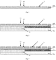
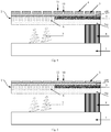
- Figs.1-4 illustrate a process of manufacturing a liquid crystal display panel according to one embodiment of the present disclosure.
- the process of manufacturing the display panel according to one embodiment of the present disclosure may be described with an example that the optical grating of the liquid crystal display panel is arranged on the outer surface of the color filter substrate.
- the intermediate layer for forming the optical grating is made of conductive materials and has light-shielding stripe patterns.
- step S10 as shown in Fig.1 , providing a transparent base substrate 100 such as a glass substrate, a quartz substrate or an organic resin substrate; forming a conductive layer 3 on the transparent base substrate 100 in such a manner that the conductive layer 3 has light-shielding stripe patterns 11 of the optical grating and light-transmitting stripe patterns 10 of the optical grating are arranged between adjacent light-shielding stripe patterns 11.
- a transparent base substrate 100 such as a glass substrate, a quartz substrate or an organic resin substrate
- a conductive film (such as ITO or IZO transparent conductive film, AI or Cu non-transparent conductive film), with a thickness of hundreds of nanometers, is deposited on the transparent base substrate 100 by means of magnetron sputtering, thermal evaporation or other methods for forming film. Then, photoresist is coated on the conductive film, and the photoresist is exposed with a mask, to form a photoresist reserved area and a photoresist unreserved area.
- the photoresist reserved area corresponds to an area where the light-shielding stripe patterns 11 are arranged, and the photoresist unreserved area corresponds to an area where the light-transmitting stripe patterns 10 are arranged.
- the conductive film in the photoresist unreserved area is etched. Finally, the remained photoresist is removed and the conductive layer 3 is formed.
- step S11 as shown in Fig.2 , forming various display film layers on a surface of the transparent base substrate 100 opposite to the transparent conductive layer 3.
- the display film layer includes a black matrix 5 configured to define a sub-pixel area; a color filter layer 6 arranged in the sub-pixel area and configured to transmit certain color; and an overcoat layer 101 covering the black matrix 5 and the color filter layer 6.
- the materials of the black matrix 5, the color filter layer 6 and the overcoat layer 101 and the manufacturing processes thereof may refer to the related art, and the description thereof is omitted herein.
- the material of the conductive layer 3 has good corrosion resistance, and thus the conductive layer 3 will not be corroded in the process of manufacturing the display film layer.
- the thickness of the formed conductive layer 3 is only hundreds of manometers, thereby guaranteeing that the transparent base substrate 100 may be absorbed firmly.
- the conductive layer 3 is connected firmly with the transparent base substrate 100 and is not easy to fall off from the transparent base substrate 100, thus the processing chamber may not be polluted.
- step S12 applying a voltage to the conductive layer 3 and spreading carbon powder 4 onto the transparent base substrate 100 and the conductive layer 3 in such a manner that the conductive layer 3 adsorbs the carbon powder 4 to form the light-shielding stripes 11, and removing unabsorbed carbon powder to form the light-transmitting stripes 10 on the transparent base substrate 100 between the light-shielding stripes 11, as shown in Fig.3 .
- step S13 as shown in Fig.4 , completing manufacturing of an array substrate 1.
- the array substrate 1 may be a thin film transistor array substrate, the manufacturing process thereof may refer to the related art, and the description thereof is omitted herein.
- Step S14 arranging oppositely the array substrate 1 and the color filter substrate 2 to form a cell; instilling liquid crystals 7 into the cell; and sealing the cell by a sealant 8, as shown in Fig.4 .
- the optical grating is on an outer surface of the color filter substrate 2.
- the liquid crystal panel may not be corroded as a result of a high temperature and being steeped in a developing solution and so on, and the liquid crystals may not be denaturized under ultraviolet light.
- the array substrate 1 first and then manufacture the color filter substrate 2. It is also feasible to perform the step S 14 first to seal the cell formed by arranging oppositely the array substrate 1 and the color filter substrate 2 as shown in Fig. 5 and then perform the step S12 to form the light-shielding stripes of the optical grating, after performing the step S11 to form the display film layers of the color filter substrate 2, so as to complete manufacturing the optical grating.
- the optical grating in the above manufacturing process may also be formed on an outer surface of the array substrate 1, as shown in Fig.6 , and the forming process thereof is similar to the above described process, and the description thereof is omitted herein.
- Figs.7-10 illustrate a process of manufacturing a liquid crystal display panel according to another embodiment of the present disclosure.
- an optical grating of a liquid crystal display panel is arranged on an outer surface of a color filter substrate, and light-transmitting stripe patterns of the optical grating are formed by an intermediate layer which is made of transparent organic material.
- a process of manufacturing the liquid crystal display panel includes following steps.
- step S20 as shown in Fig.7 , providing a transparent base substrate 100 such as a glass substrate, a quartz substrate or an organic resin substrate; forming a transparent organic layer 3 on the transparent base substrate 100 in such a manner that the transparent organic layer 3 has light-transmitting stripes 10 of an optical grating and light-shielding stripe patterns 11 of the optical grating are arranged between adjacent light-transmitting stripe patterns 10.
- a transparent base substrate 100 such as a glass substrate, a quartz substrate or an organic resin substrate
- step S21 as shown in Fig.8 , forming various display film layers on a surface of the transparent base substrate 100 opposite to the transparent organic layer 3.
- step S22 rubbing a surface of the transparent base substrate 100 where the transparent organic layer 3 is formed to make the surface charged; spreading carbon powder 4 onto the transparent base substrate 100 and the transparent organic layer 3, so that the charged transparent base substrate 100 adsorbs the carbon powder 4 to form the light-shielding stripes 11; after removing the unabsorbed carbon powder, the uncharged transparent organic layer 3 forms the light-transmitting stripes 10, as shown in Fig.9 .
- step S23 completing manufacturing of an array substrate 1, as shown in Fig.10 .
- step S24 arranging oppositely the array substrate 1 and the color filter substrate 2 to form a cell; instilling liquid crystals 7 into the cell; and sealing the cell by a sealant 8, as shown in Fig.10 .
- the manufacturing of the liquid display panel is completed, and the optical grating is on an outer surface of the color filter substrate 2.
- the array substrate 1 first and then manufacture the color filter substrate 2. It is also feasible to perform the step S24 first to seal the cell formed by arranging oppositely the array substrate 1 and the color filter substrate 2 as shown in Fig.11 and then perform the step S22 to forming the light-shielding stripes of the optical grating, after performing the step S21 to form the display film layers of the color filter substrate 2, so as to complete manufacturing of the optical grating.
- the optical grating in the above manufacturing process may also be formed on an outer surface of the array substrate 1, as shown in Fig.12 , the forming process thereof is similar to the above described process, and the description thereof is omitted herein.
- the technical solution of the present disclosure is also applicable to an organic light emitting diode display panel, and the process of manufacturing an optical grating therein is similar to the process of manufacturing the optical grating in the liquid crystal display panel, and the difference between the two processes only lies in that an display film layer of the organic light emitting diode display panel includes a negative electrode, a hole-injection layer, a hole-transport layer, an electron-injection layer, an electron-transport layer, a positive electrode, etc, and the manufacturing process thereof may refer to the related art.
- a display device is further provided in the present disclosure, including the above display panel, to improve yields of a three-dimensional display device and a dual-field-of-view display device.
- the intermediate layer of stable property is first used to form the stripe patterns arranged at intervals on the outer surface of the transparent base substrate; then, various display film layers are formed on the inner surface of the transparent base substrate where the intermediate layer is formed; finally, the opaque material is absorbed onto the surface of the intermediate layer or into intervals of the intermediate layer on the transparent base substrate, to form light-shielding stripes and light-transmitting stripes of the optical grating which are alternately arranged.
- the intermediate layer does not need a low enough transmittance, so it is relatively thin, so that the base substrate can be absorbed firmly when forming the display film layers.
- the processing chamber may not be polluted by the intermediate layer. Therefore, the process of manufacturing the optical grating may not influence the process of manufacturing the display film layer.
Landscapes
- Physics & Mathematics (AREA)
- Nonlinear Science (AREA)
- Optics & Photonics (AREA)
- General Physics & Mathematics (AREA)
- Mathematical Physics (AREA)
- Chemical & Material Sciences (AREA)
- Crystallography & Structural Chemistry (AREA)
- Optical Filters (AREA)
- Electroluminescent Light Sources (AREA)
- Printing Plates And Materials Therefor (AREA)
- Printing Methods (AREA)
Applications Claiming Priority (2)
| Application Number | Priority Date | Filing Date | Title |
|---|---|---|---|
| CN201410696890.4A CN104460100B (zh) | 2014-11-26 | 2014-11-26 | 显示基板和显示面板及其制作方法、显示装置 |
| PCT/CN2015/075197 WO2016082396A1 (fr) | 2014-11-26 | 2015-03-27 | Substrat d'affichage, panneau d'affichage, son procédé de fabrication et dispositif d'affichage |
Publications (3)
| Publication Number | Publication Date |
|---|---|
| EP3226071A1 true EP3226071A1 (fr) | 2017-10-04 |
| EP3226071A4 EP3226071A4 (fr) | 2018-07-25 |
| EP3226071B1 EP3226071B1 (fr) | 2019-09-11 |
Family
ID=52906398
Family Applications (1)
| Application Number | Title | Priority Date | Filing Date |
|---|---|---|---|
| EP15766038.2A Active EP3226071B1 (fr) | 2014-11-26 | 2015-03-27 | Substrat d'affichage, panneau d'affichage, son procédé de fabrication et dispositif d'affichage |
Country Status (4)
| Country | Link |
|---|---|
| US (1) | US10488563B2 (fr) |
| EP (1) | EP3226071B1 (fr) |
| CN (1) | CN104460100B (fr) |
| WO (1) | WO2016082396A1 (fr) |
Families Citing this family (4)
| Publication number | Priority date | Publication date | Assignee | Title |
|---|---|---|---|---|
| CN104460100B (zh) * | 2014-11-26 | 2018-03-27 | 京东方科技集团股份有限公司 | 显示基板和显示面板及其制作方法、显示装置 |
| CN104977724A (zh) * | 2015-07-13 | 2015-10-14 | 深圳市华星光电技术有限公司 | 3d显示装置及其制作方法 |
| CN110085133A (zh) * | 2018-01-26 | 2019-08-02 | 京东方科技集团股份有限公司 | 显示基板及其制作方法、显示面板和显示装置 |
| US11119370B2 (en) * | 2018-01-29 | 2021-09-14 | Himax Display, Inc. | Display panel |
Family Cites Families (20)
| Publication number | Priority date | Publication date | Assignee | Title |
|---|---|---|---|---|
| US20080158500A1 (en) * | 2006-12-27 | 2008-07-03 | Yasushi Kawata | Display Device and Method for Manufacturing the Same |
| DE102008060279B4 (de) * | 2007-12-05 | 2023-09-14 | Lg Display Co., Ltd. | Multiansicht-Anzeigevorrichtung |
| US20090152533A1 (en) | 2007-12-17 | 2009-06-18 | Winston Kong Chan | Increasing the external efficiency of light emitting diodes |
| EP2296889B1 (fr) | 2008-06-16 | 2015-04-01 | Humaneyes Technologies Ltd. | Dispositif et procédé de traitement d un substrat d impression lenticulaire |
| CN101561571A (zh) * | 2009-05-14 | 2009-10-21 | 深圳华映显示科技有限公司 | 一种液晶显示面板及液晶显示装置 |
| JP5567855B2 (ja) * | 2010-02-16 | 2014-08-06 | 株式会社ジャパンディスプレイ | 表示装置および電子機器 |
| EP2564247A2 (fr) * | 2010-04-27 | 2013-03-06 | The Regents Of The University Of Michigan | Dispositif d'affichage ayant des filtres de couleur plasmoniques et ayant des capacités photovoltaïques |
| CN102236201B (zh) * | 2010-04-30 | 2014-06-04 | 京东方科技集团股份有限公司 | 双视显示器、双视彩膜结构及其制造方法 |
| TW201215916A (en) * | 2010-10-01 | 2012-04-16 | J Touch Corp | Display device structure improvement featuring 2D/3D image switching |
| GB2487944B (en) * | 2011-02-09 | 2018-02-21 | Spice Application Systems Ltd | A comestible product coating delivery method and apparatus |
| CN102681176B (zh) * | 2011-03-18 | 2014-01-08 | 介面光电股份有限公司 | 3d显示器及其光栅装置的制造方法 |
| CN202008551U (zh) * | 2011-04-14 | 2011-10-12 | 京东方科技集团股份有限公司 | 一种双视显示面板 |
| JP5962229B2 (ja) * | 2012-06-05 | 2016-08-03 | 三菱電機株式会社 | 表示装置 |
| CN102768424B (zh) * | 2012-07-02 | 2014-07-09 | 京东方科技集团股份有限公司 | 双视角显示面板及其制造方法 |
| CN202895860U (zh) * | 2012-11-08 | 2013-04-24 | 江阴通利光电科技有限公司 | 一种新型3d光学立体膜片 |
| CN202904128U (zh) | 2012-11-08 | 2013-04-24 | 江阴通利光电科技有限公司 | 一种新型3d的光学立体膜片 |
| CN102981196A (zh) | 2012-12-11 | 2013-03-20 | 南京中电熊猫液晶显示科技有限公司 | 柱透镜光栅、光栅视差屏障式立体显示装置及视差屏障 |
| CN103454807B (zh) * | 2013-09-02 | 2016-07-27 | 京东方科技集团股份有限公司 | 阵列基板及其制作方法、3d显示装置 |
| CN203773156U (zh) * | 2014-04-11 | 2014-08-13 | 京东方科技集团股份有限公司 | 一种光栅结构及显示装置 |
| CN104460100B (zh) | 2014-11-26 | 2018-03-27 | 京东方科技集团股份有限公司 | 显示基板和显示面板及其制作方法、显示装置 |
-
2014
- 2014-11-26 CN CN201410696890.4A patent/CN104460100B/zh not_active Expired - Fee Related
-
2015
- 2015-03-27 EP EP15766038.2A patent/EP3226071B1/fr active Active
- 2015-03-27 WO PCT/CN2015/075197 patent/WO2016082396A1/fr not_active Ceased
- 2015-03-27 US US14/780,399 patent/US10488563B2/en not_active Expired - Fee Related
Also Published As
| Publication number | Publication date |
|---|---|
| WO2016082396A1 (fr) | 2016-06-02 |
| US20160327693A1 (en) | 2016-11-10 |
| EP3226071B1 (fr) | 2019-09-11 |
| CN104460100B (zh) | 2018-03-27 |
| CN104460100A (zh) | 2015-03-25 |
| EP3226071A4 (fr) | 2018-07-25 |
| US10488563B2 (en) | 2019-11-26 |
Similar Documents
| Publication | Publication Date | Title |
|---|---|---|
| EP2720079B1 (fr) | Dispositif d'affichage à cristaux liquides et procédé de fabrication correspondant | |
| US9329445B2 (en) | Mask plate and processes for manufacturing ultraviolet mask plate and array substrate | |
| US8953136B2 (en) | Color filter substrate, liquid crystal display device including color filter substrate, and method of fabricating color filter substrate | |
| KR102003269B1 (ko) | 광학 필터의 제조 방법 및 광학 필터를 구비하는 유기 발광 표시 장치의 제조 방법 | |
| US9488871B2 (en) | Method for manufacturing display panel | |
| CN103018968B (zh) | 一种封框胶的固化方法 | |
| CN103646852B (zh) | 一种基板的制作方法 | |
| EP3226071B1 (fr) | Substrat d'affichage, panneau d'affichage, son procédé de fabrication et dispositif d'affichage | |
| JP5538106B2 (ja) | 液晶表示パネル | |
| CN105739185A (zh) | 液晶面板的制作方法和液晶面板 | |
| KR102090176B1 (ko) | 주름 구조의 전극, 이를 포함하는 표시 장치 및 이의 제조 방법 | |
| US20130321719A1 (en) | Electronic device and method for manufacturing same | |
| US20160109738A1 (en) | Display panel and method of manufacturing the same | |
| KR101243395B1 (ko) | 유기 박막 트랜지스터 어레이 기판 및 그 제조 방법 | |
| KR20130106664A (ko) | 플렉서블 액정 표시 장치의 제조 방법 | |
| KR102484136B1 (ko) | 표시 기판, 이를 포함하는 액정 표시 장치, 및 이의 제조 방법 | |
| CN203930286U (zh) | 母板堆叠结构 | |
| US20110221990A1 (en) | Display device and method of manufacturing the same | |
| US20160155992A1 (en) | Display substrate and manufacturing method thereof and display device | |
| KR20120076708A (ko) | 디스플레이 패널용 모기판 및 디스플레이 패널 제조방법 | |
| CN109637353B (zh) | 显示基板及其制作方法、显示面板及其制作方法、装置 | |
| US9312324B2 (en) | Organic thin film transistor comprising banks, organic thin film transistor array substrate and display device | |
| KR20160034120A (ko) | 나노와이어를 이용한 투명 전극 기판 제조방법과 이를 이용한 투명 전극 기판 및 터치패널 | |
| KR102851187B1 (ko) | 광 경로 제어 장치 및 그의 제조 방법 | |
| US20150316801A1 (en) | Display panel structure and manufacturing method thereof |
Legal Events
| Date | Code | Title | Description |
|---|---|---|---|
| STAA | Information on the status of an ep patent application or granted ep patent |
Free format text: STATUS: THE INTERNATIONAL PUBLICATION HAS BEEN MADE |
|
| PUAI | Public reference made under article 153(3) epc to a published international application that has entered the european phase |
Free format text: ORIGINAL CODE: 0009012 |
|
| STAA | Information on the status of an ep patent application or granted ep patent |
Free format text: STATUS: REQUEST FOR EXAMINATION WAS MADE |
|
| 17P | Request for examination filed |
Effective date: 20150925 |
|
| AK | Designated contracting states |
Kind code of ref document: A1 Designated state(s): AL AT BE BG CH CY CZ DE DK EE ES FI FR GB GR HR HU IE IS IT LI LT LU LV MC MK MT NL NO PL PT RO RS SE SI SK SM TR |
|
| AX | Request for extension of the european patent |
Extension state: BA ME |
|
| DAV | Request for validation of the european patent (deleted) | ||
| DAX | Request for extension of the european patent (deleted) | ||
| A4 | Supplementary search report drawn up and despatched |
Effective date: 20180627 |
|
| RIC1 | Information provided on ipc code assigned before grant |
Ipc: G02F 1/1335 20060101AFI20180621BHEP |
|
| GRAP | Despatch of communication of intention to grant a patent |
Free format text: ORIGINAL CODE: EPIDOSNIGR1 |
|
| STAA | Information on the status of an ep patent application or granted ep patent |
Free format text: STATUS: GRANT OF PATENT IS INTENDED |
|
| INTG | Intention to grant announced |
Effective date: 20190417 |
|
| GRAS | Grant fee paid |
Free format text: ORIGINAL CODE: EPIDOSNIGR3 |
|
| GRAA | (expected) grant |
Free format text: ORIGINAL CODE: 0009210 |
|
| STAA | Information on the status of an ep patent application or granted ep patent |
Free format text: STATUS: THE PATENT HAS BEEN GRANTED |
|
| AK | Designated contracting states |
Kind code of ref document: B1 Designated state(s): AL AT BE BG CH CY CZ DE DK EE ES FI FR GB GR HR HU IE IS IT LI LT LU LV MC MK MT NL NO PL PT RO RS SE SI SK SM TR |
|
| REG | Reference to a national code |
Ref country code: GB Ref legal event code: FG4D |
|
| REG | Reference to a national code |
Ref country code: CH Ref legal event code: EP |
|
| REG | Reference to a national code |
Ref country code: AT Ref legal event code: REF Ref document number: 1179205 Country of ref document: AT Kind code of ref document: T Effective date: 20190915 |
|
| REG | Reference to a national code |
Ref country code: DE Ref legal event code: R096 Ref document number: 602015037845 Country of ref document: DE Ref country code: IE Ref legal event code: FG4D |
|
| REG | Reference to a national code |
Ref country code: NL Ref legal event code: MP Effective date: 20190911 |
|
| REG | Reference to a national code |
Ref country code: LT Ref legal event code: MG4D |
|
| PG25 | Lapsed in a contracting state [announced via postgrant information from national office to epo] |
Ref country code: FI Free format text: LAPSE BECAUSE OF FAILURE TO SUBMIT A TRANSLATION OF THE DESCRIPTION OR TO PAY THE FEE WITHIN THE PRESCRIBED TIME-LIMIT Effective date: 20190911 Ref country code: NO Free format text: LAPSE BECAUSE OF FAILURE TO SUBMIT A TRANSLATION OF THE DESCRIPTION OR TO PAY THE FEE WITHIN THE PRESCRIBED TIME-LIMIT Effective date: 20191211 Ref country code: BG Free format text: LAPSE BECAUSE OF FAILURE TO SUBMIT A TRANSLATION OF THE DESCRIPTION OR TO PAY THE FEE WITHIN THE PRESCRIBED TIME-LIMIT Effective date: 20191211 Ref country code: SE Free format text: LAPSE BECAUSE OF FAILURE TO SUBMIT A TRANSLATION OF THE DESCRIPTION OR TO PAY THE FEE WITHIN THE PRESCRIBED TIME-LIMIT Effective date: 20190911 Ref country code: LT Free format text: LAPSE BECAUSE OF FAILURE TO SUBMIT A TRANSLATION OF THE DESCRIPTION OR TO PAY THE FEE WITHIN THE PRESCRIBED TIME-LIMIT Effective date: 20190911 Ref country code: HR Free format text: LAPSE BECAUSE OF FAILURE TO SUBMIT A TRANSLATION OF THE DESCRIPTION OR TO PAY THE FEE WITHIN THE PRESCRIBED TIME-LIMIT Effective date: 20190911 |
|
| PG25 | Lapsed in a contracting state [announced via postgrant information from national office to epo] |
Ref country code: RS Free format text: LAPSE BECAUSE OF FAILURE TO SUBMIT A TRANSLATION OF THE DESCRIPTION OR TO PAY THE FEE WITHIN THE PRESCRIBED TIME-LIMIT Effective date: 20190911 Ref country code: LV Free format text: LAPSE BECAUSE OF FAILURE TO SUBMIT A TRANSLATION OF THE DESCRIPTION OR TO PAY THE FEE WITHIN THE PRESCRIBED TIME-LIMIT Effective date: 20190911 Ref country code: AL Free format text: LAPSE BECAUSE OF FAILURE TO SUBMIT A TRANSLATION OF THE DESCRIPTION OR TO PAY THE FEE WITHIN THE PRESCRIBED TIME-LIMIT Effective date: 20190911 Ref country code: ES Free format text: LAPSE BECAUSE OF FAILURE TO SUBMIT A TRANSLATION OF THE DESCRIPTION OR TO PAY THE FEE WITHIN THE PRESCRIBED TIME-LIMIT Effective date: 20190911 Ref country code: GR Free format text: LAPSE BECAUSE OF FAILURE TO SUBMIT A TRANSLATION OF THE DESCRIPTION OR TO PAY THE FEE WITHIN THE PRESCRIBED TIME-LIMIT Effective date: 20191212 |
|
| REG | Reference to a national code |
Ref country code: AT Ref legal event code: MK05 Ref document number: 1179205 Country of ref document: AT Kind code of ref document: T Effective date: 20190911 |
|
| PG25 | Lapsed in a contracting state [announced via postgrant information from national office to epo] |
Ref country code: EE Free format text: LAPSE BECAUSE OF FAILURE TO SUBMIT A TRANSLATION OF THE DESCRIPTION OR TO PAY THE FEE WITHIN THE PRESCRIBED TIME-LIMIT Effective date: 20190911 Ref country code: PL Free format text: LAPSE BECAUSE OF FAILURE TO SUBMIT A TRANSLATION OF THE DESCRIPTION OR TO PAY THE FEE WITHIN THE PRESCRIBED TIME-LIMIT Effective date: 20190911 Ref country code: PT Free format text: LAPSE BECAUSE OF FAILURE TO SUBMIT A TRANSLATION OF THE DESCRIPTION OR TO PAY THE FEE WITHIN THE PRESCRIBED TIME-LIMIT Effective date: 20200113 Ref country code: IT Free format text: LAPSE BECAUSE OF FAILURE TO SUBMIT A TRANSLATION OF THE DESCRIPTION OR TO PAY THE FEE WITHIN THE PRESCRIBED TIME-LIMIT Effective date: 20190911 Ref country code: RO Free format text: LAPSE BECAUSE OF FAILURE TO SUBMIT A TRANSLATION OF THE DESCRIPTION OR TO PAY THE FEE WITHIN THE PRESCRIBED TIME-LIMIT Effective date: 20190911 Ref country code: AT Free format text: LAPSE BECAUSE OF FAILURE TO SUBMIT A TRANSLATION OF THE DESCRIPTION OR TO PAY THE FEE WITHIN THE PRESCRIBED TIME-LIMIT Effective date: 20190911 Ref country code: NL Free format text: LAPSE BECAUSE OF FAILURE TO SUBMIT A TRANSLATION OF THE DESCRIPTION OR TO PAY THE FEE WITHIN THE PRESCRIBED TIME-LIMIT Effective date: 20190911 |
|
| PG25 | Lapsed in a contracting state [announced via postgrant information from national office to epo] |
Ref country code: SK Free format text: LAPSE BECAUSE OF FAILURE TO SUBMIT A TRANSLATION OF THE DESCRIPTION OR TO PAY THE FEE WITHIN THE PRESCRIBED TIME-LIMIT Effective date: 20190911 Ref country code: SM Free format text: LAPSE BECAUSE OF FAILURE TO SUBMIT A TRANSLATION OF THE DESCRIPTION OR TO PAY THE FEE WITHIN THE PRESCRIBED TIME-LIMIT Effective date: 20190911 Ref country code: CZ Free format text: LAPSE BECAUSE OF FAILURE TO SUBMIT A TRANSLATION OF THE DESCRIPTION OR TO PAY THE FEE WITHIN THE PRESCRIBED TIME-LIMIT Effective date: 20190911 Ref country code: IS Free format text: LAPSE BECAUSE OF FAILURE TO SUBMIT A TRANSLATION OF THE DESCRIPTION OR TO PAY THE FEE WITHIN THE PRESCRIBED TIME-LIMIT Effective date: 20200224 |
|
| REG | Reference to a national code |
Ref country code: DE Ref legal event code: R097 Ref document number: 602015037845 Country of ref document: DE |
|
| PLBE | No opposition filed within time limit |
Free format text: ORIGINAL CODE: 0009261 |
|
| STAA | Information on the status of an ep patent application or granted ep patent |
Free format text: STATUS: NO OPPOSITION FILED WITHIN TIME LIMIT |
|
| PG2D | Information on lapse in contracting state deleted |
Ref country code: IS |
|
| PG25 | Lapsed in a contracting state [announced via postgrant information from national office to epo] |
Ref country code: DK Free format text: LAPSE BECAUSE OF FAILURE TO SUBMIT A TRANSLATION OF THE DESCRIPTION OR TO PAY THE FEE WITHIN THE PRESCRIBED TIME-LIMIT Effective date: 20190911 Ref country code: IS Free format text: LAPSE BECAUSE OF FAILURE TO SUBMIT A TRANSLATION OF THE DESCRIPTION OR TO PAY THE FEE WITHIN THE PRESCRIBED TIME-LIMIT Effective date: 20200112 |
|
| 26N | No opposition filed |
Effective date: 20200615 |
|
| PG25 | Lapsed in a contracting state [announced via postgrant information from national office to epo] |
Ref country code: SI Free format text: LAPSE BECAUSE OF FAILURE TO SUBMIT A TRANSLATION OF THE DESCRIPTION OR TO PAY THE FEE WITHIN THE PRESCRIBED TIME-LIMIT Effective date: 20190911 |
|
| PG25 | Lapsed in a contracting state [announced via postgrant information from national office to epo] |
Ref country code: MC Free format text: LAPSE BECAUSE OF FAILURE TO SUBMIT A TRANSLATION OF THE DESCRIPTION OR TO PAY THE FEE WITHIN THE PRESCRIBED TIME-LIMIT Effective date: 20190911 |
|
| REG | Reference to a national code |
Ref country code: CH Ref legal event code: PL |
|
| REG | Reference to a national code |
Ref country code: BE Ref legal event code: MM Effective date: 20200331 |
|
| PG25 | Lapsed in a contracting state [announced via postgrant information from national office to epo] |
Ref country code: LU Free format text: LAPSE BECAUSE OF NON-PAYMENT OF DUE FEES Effective date: 20200327 |
|
| PG25 | Lapsed in a contracting state [announced via postgrant information from national office to epo] |
Ref country code: IE Free format text: LAPSE BECAUSE OF NON-PAYMENT OF DUE FEES Effective date: 20200327 Ref country code: LI Free format text: LAPSE BECAUSE OF NON-PAYMENT OF DUE FEES Effective date: 20200331 Ref country code: CH Free format text: LAPSE BECAUSE OF NON-PAYMENT OF DUE FEES Effective date: 20200331 |
|
| PG25 | Lapsed in a contracting state [announced via postgrant information from national office to epo] |
Ref country code: BE Free format text: LAPSE BECAUSE OF NON-PAYMENT OF DUE FEES Effective date: 20200331 |
|
| PGFP | Annual fee paid to national office [announced via postgrant information from national office to epo] |
Ref country code: FR Payment date: 20210324 Year of fee payment: 7 |
|
| PGFP | Annual fee paid to national office [announced via postgrant information from national office to epo] |
Ref country code: GB Payment date: 20210324 Year of fee payment: 7 Ref country code: DE Payment date: 20210319 Year of fee payment: 7 |
|
| PG25 | Lapsed in a contracting state [announced via postgrant information from national office to epo] |
Ref country code: TR Free format text: LAPSE BECAUSE OF FAILURE TO SUBMIT A TRANSLATION OF THE DESCRIPTION OR TO PAY THE FEE WITHIN THE PRESCRIBED TIME-LIMIT Effective date: 20190911 Ref country code: MT Free format text: LAPSE BECAUSE OF FAILURE TO SUBMIT A TRANSLATION OF THE DESCRIPTION OR TO PAY THE FEE WITHIN THE PRESCRIBED TIME-LIMIT Effective date: 20190911 Ref country code: CY Free format text: LAPSE BECAUSE OF FAILURE TO SUBMIT A TRANSLATION OF THE DESCRIPTION OR TO PAY THE FEE WITHIN THE PRESCRIBED TIME-LIMIT Effective date: 20190911 |
|
| PG25 | Lapsed in a contracting state [announced via postgrant information from national office to epo] |
Ref country code: MK Free format text: LAPSE BECAUSE OF FAILURE TO SUBMIT A TRANSLATION OF THE DESCRIPTION OR TO PAY THE FEE WITHIN THE PRESCRIBED TIME-LIMIT Effective date: 20190911 |
|
| REG | Reference to a national code |
Ref country code: DE Ref legal event code: R119 Ref document number: 602015037845 Country of ref document: DE |
|
| GBPC | Gb: european patent ceased through non-payment of renewal fee |
Effective date: 20220327 |
|
| PG25 | Lapsed in a contracting state [announced via postgrant information from national office to epo] |
Ref country code: GB Free format text: LAPSE BECAUSE OF NON-PAYMENT OF DUE FEES Effective date: 20220327 Ref country code: FR Free format text: LAPSE BECAUSE OF NON-PAYMENT OF DUE FEES Effective date: 20220331 Ref country code: DE Free format text: LAPSE BECAUSE OF NON-PAYMENT OF DUE FEES Effective date: 20221001 |