EP3227121B1 - Druckkopf - Google Patents
Druckkopf Download PDFInfo
- Publication number
- EP3227121B1 EP3227121B1 EP14907213.4A EP14907213A EP3227121B1 EP 3227121 B1 EP3227121 B1 EP 3227121B1 EP 14907213 A EP14907213 A EP 14907213A EP 3227121 B1 EP3227121 B1 EP 3227121B1
- Authority
- EP
- European Patent Office
- Prior art keywords
- drive circuit
- printhead
- circuit components
- nozzle
- energy delivery
- Prior art date
- Legal status (The legal status is an assumption and is not a legal conclusion. Google has not performed a legal analysis and makes no representation as to the accuracy of the status listed.)
- Not-in-force
Links
- 230000004913 activation Effects 0.000 claims description 38
- 239000012530 fluid Substances 0.000 claims description 36
- 238000000034 method Methods 0.000 claims description 25
- 238000004519 manufacturing process Methods 0.000 claims description 8
- 230000003213 activating effect Effects 0.000 claims description 7
- 230000008878 coupling Effects 0.000 claims description 6
- 238000010168 coupling process Methods 0.000 claims description 6
- 238000005859 coupling reaction Methods 0.000 claims description 6
- 230000001419 dependent effect Effects 0.000 claims description 2
- 238000010586 diagram Methods 0.000 description 16
- 238000010304 firing Methods 0.000 description 10
- 239000004065 semiconductor Substances 0.000 description 10
- 238000010438 heat treatment Methods 0.000 description 7
- 230000008569 process Effects 0.000 description 5
- 230000004048 modification Effects 0.000 description 4
- 238000012986 modification Methods 0.000 description 4
- 238000005516 engineering process Methods 0.000 description 3
- 239000000463 material Substances 0.000 description 3
- 230000008859 change Effects 0.000 description 2
- 238000007667 floating Methods 0.000 description 2
- 230000004044 response Effects 0.000 description 2
- 238000010146 3D printing Methods 0.000 description 1
- 230000009286 beneficial effect Effects 0.000 description 1
- 230000005540 biological transmission Effects 0.000 description 1
- 239000003990 capacitor Substances 0.000 description 1
- 230000005465 channeling Effects 0.000 description 1
- 230000008021 deposition Effects 0.000 description 1
- 239000002305 electric material Substances 0.000 description 1
- 230000005669 field effect Effects 0.000 description 1
- 238000000059 patterning Methods 0.000 description 1
- 238000007639 printing Methods 0.000 description 1
- 229910052710 silicon Inorganic materials 0.000 description 1
- 239000010703 silicon Substances 0.000 description 1
- 229920001169 thermoplastic Polymers 0.000 description 1
- 239000004416 thermosoftening plastic Substances 0.000 description 1
- 239000010409 thin film Substances 0.000 description 1
- 238000004448 titration Methods 0.000 description 1
- 230000001960 triggered effect Effects 0.000 description 1
Images




Classifications
-
- B—PERFORMING OPERATIONS; TRANSPORTING
- B41—PRINTING; LINING MACHINES; TYPEWRITERS; STAMPS
- B41J—TYPEWRITERS; SELECTIVE PRINTING MECHANISMS, i.e. MECHANISMS PRINTING OTHERWISE THAN FROM A FORME; CORRECTION OF TYPOGRAPHICAL ERRORS
- B41J2/00—Typewriters or selective printing mechanisms characterised by the printing or marking process for which they are designed
- B41J2/005—Typewriters or selective printing mechanisms characterised by the printing or marking process for which they are designed characterised by bringing liquid or particles selectively into contact with a printing material
- B41J2/01—Ink jet
- B41J2/015—Ink jet characterised by the jet generation process
- B41J2/04—Ink jet characterised by the jet generation process generating single droplets or particles on demand
- B41J2/045—Ink jet characterised by the jet generation process generating single droplets or particles on demand by pressure, e.g. electromechanical transducers
- B41J2/04501—Control methods or devices therefor, e.g. driver circuits, control circuits
- B41J2/04541—Specific driving circuit
-
- B—PERFORMING OPERATIONS; TRANSPORTING
- B41—PRINTING; LINING MACHINES; TYPEWRITERS; STAMPS
- B41J—TYPEWRITERS; SELECTIVE PRINTING MECHANISMS, i.e. MECHANISMS PRINTING OTHERWISE THAN FROM A FORME; CORRECTION OF TYPOGRAPHICAL ERRORS
- B41J2/00—Typewriters or selective printing mechanisms characterised by the printing or marking process for which they are designed
- B41J2/005—Typewriters or selective printing mechanisms characterised by the printing or marking process for which they are designed characterised by bringing liquid or particles selectively into contact with a printing material
- B41J2/01—Ink jet
- B41J2/015—Ink jet characterised by the jet generation process
- B41J2/04—Ink jet characterised by the jet generation process generating single droplets or particles on demand
- B41J2/045—Ink jet characterised by the jet generation process generating single droplets or particles on demand by pressure, e.g. electromechanical transducers
- B41J2/04501—Control methods or devices therefor, e.g. driver circuits, control circuits
- B41J2/04548—Details of power line section of control circuit
-
- B—PERFORMING OPERATIONS; TRANSPORTING
- B41—PRINTING; LINING MACHINES; TYPEWRITERS; STAMPS
- B41J—TYPEWRITERS; SELECTIVE PRINTING MECHANISMS, i.e. MECHANISMS PRINTING OTHERWISE THAN FROM A FORME; CORRECTION OF TYPOGRAPHICAL ERRORS
- B41J2/00—Typewriters or selective printing mechanisms characterised by the printing or marking process for which they are designed
- B41J2/005—Typewriters or selective printing mechanisms characterised by the printing or marking process for which they are designed characterised by bringing liquid or particles selectively into contact with a printing material
- B41J2/01—Ink jet
- B41J2/015—Ink jet characterised by the jet generation process
- B41J2/04—Ink jet characterised by the jet generation process generating single droplets or particles on demand
- B41J2/045—Ink jet characterised by the jet generation process generating single droplets or particles on demand by pressure, e.g. electromechanical transducers
- B41J2/04501—Control methods or devices therefor, e.g. driver circuits, control circuits
- B41J2/0455—Details of switching sections of circuit, e.g. transistors
-
- B—PERFORMING OPERATIONS; TRANSPORTING
- B41—PRINTING; LINING MACHINES; TYPEWRITERS; STAMPS
- B41J—TYPEWRITERS; SELECTIVE PRINTING MECHANISMS, i.e. MECHANISMS PRINTING OTHERWISE THAN FROM A FORME; CORRECTION OF TYPOGRAPHICAL ERRORS
- B41J2/00—Typewriters or selective printing mechanisms characterised by the printing or marking process for which they are designed
- B41J2/005—Typewriters or selective printing mechanisms characterised by the printing or marking process for which they are designed characterised by bringing liquid or particles selectively into contact with a printing material
- B41J2/01—Ink jet
- B41J2/015—Ink jet characterised by the jet generation process
- B41J2/04—Ink jet characterised by the jet generation process generating single droplets or particles on demand
- B41J2/045—Ink jet characterised by the jet generation process generating single droplets or particles on demand by pressure, e.g. electromechanical transducers
- B41J2/04501—Control methods or devices therefor, e.g. driver circuits, control circuits
- B41J2/0458—Control methods or devices therefor, e.g. driver circuits, control circuits controlling heads based on heating elements forming bubbles
-
- B—PERFORMING OPERATIONS; TRANSPORTING
- B41—PRINTING; LINING MACHINES; TYPEWRITERS; STAMPS
- B41J—TYPEWRITERS; SELECTIVE PRINTING MECHANISMS, i.e. MECHANISMS PRINTING OTHERWISE THAN FROM A FORME; CORRECTION OF TYPOGRAPHICAL ERRORS
- B41J2/00—Typewriters or selective printing mechanisms characterised by the printing or marking process for which they are designed
- B41J2/005—Typewriters or selective printing mechanisms characterised by the printing or marking process for which they are designed characterised by bringing liquid or particles selectively into contact with a printing material
- B41J2/01—Ink jet
- B41J2/07—Ink jet characterised by jet control
-
- B—PERFORMING OPERATIONS; TRANSPORTING
- B41—PRINTING; LINING MACHINES; TYPEWRITERS; STAMPS
- B41J—TYPEWRITERS; SELECTIVE PRINTING MECHANISMS, i.e. MECHANISMS PRINTING OTHERWISE THAN FROM A FORME; CORRECTION OF TYPOGRAPHICAL ERRORS
- B41J2202/00—Embodiments of or processes related to ink-jet or thermal heads
- B41J2202/01—Embodiments of or processes related to ink-jet heads
- B41J2202/13—Heads having an integrated circuit
Definitions
- Today's printers generally use a fluid delivery system that includes some form of printhead.
- the printhead holds a reservoir of fluid, such as ink, along with circuitry that enables the fluid to be ejected onto a print medium through nozzles.
- Some printheads are configured to be easily refilled, while others are intended for disposal after a single-use.
- the printhead usually is inserted into a carriage of a printer such that electrical contacts on the printhead couple to electrical outputs from the printer. Electrical control signals from the printer activate the nozzles to eject fluid and control which nozzles are activated and the timing of the activation.
- a substantial amount of circuitry may be included in the printhead to enable control signals from the printer to be properly processed.
- EP1080898A2 relates to a printhead incorporating multiple address bus demultiplexing circuitry for driving drop ejector heater resistors, where redundant control lines for the heating elements increase the printhead's reliability.
- US2005/0140710A1 discloses driving a printhead with a plurality of address lines and control lines controlling the heating elements.
- EP1849604A2 relates to a printhead control circuit for driving a heating resistor to fire droplets of ink.
- printheads often include substantial amounts of circuitry used to drive the activation of nozzles.
- the drive circuitry can include a circuit layer and an interconnect layer.
- the circuit layer includes a number of drive circuit components such as logic gates, transistors, resistors, capacitors, and the like, which are fabricated in a semiconductor wafer using semiconductor fabrication techniques.
- the interconnect layer conductive traces formed over the semiconductor of the circuit layer to couple the drive circuit components.
- the fluidic layers which include the fluid chambers and nozzles, are usually fabricated on top of the drive circuitry.
- the techniques described herein enable a single drive circuit component layout to be used in the fabrication of printheads with different nozzle densities. This enables the printhead nozzle density to be scaled without modifying the layout of the drive circuit components fabricated in the semiconductor. Additionally, in printheads with reduced nozzle density, the same drive circuit component layout can be used to increase the power used for driving fluid ejection.
- the drive circuit component layout is re-used with multiple printhead designs by changing the design of the interconnect layer. This allows for one standard circuit layer to be used in the fabrication of different types of printheads with different fluidic layouts, thereby serving a wider product range at lower cost.
- Fig. 1 is a diagram of the bottom surface of an example printhead.
- the printhead is generally referred to by the reference number 100.
- the printhead 100 of Fig. 1 includes a fluid feed slot 102 and two columns of nozzles 104, referred to as nozzle columns 106.
- fluid is drawn from the fluid feed slot 102 and ejected from the nozzles 104 onto a print medium.
- the fluid may be ink, a material used in three-dimensional printing such as a thermoplastic or photopolymer, or other suitable fluid.
- Each nozzle 104 may be part of a fluid chamber that includes an adjacent energy delivery device, which is activated by an activation device.
- the activation devices are referred to herein as transistors 110 and the energy delivery devices are heating elements, which are referred to herein as resistors 108.
- the activation devices may any suitable type of transistors such Field Effect Transistors (FETs), switches such as Micro-Electro-Mechanical System (MEMS) switches, and others.
- FETs Field Effect Transistors
- MEMS Micro-Electro-Mechanical System
- Each resistor 108 is electrically coupled to the output of at least one transistor 110, which provides the current to the resistor 108, causing the resistor 108 to generate heat.
- a selected nozzle 104 can be activated by turning on the corresponding transistors 110, which heats the fluid in contact with or adjacent to the resistor 108 and thereby causes the fluid to be ejected from the nozzle 104.
- the current is delivered to the resistor 108 in a series of pulses.
- the transistor 110 is part of the drive circuitry of the printhead 100. Other components of the drive circuitry will be described in later figures.
- the resistors 108, nozzles 104, fluid feed slot 102, and other fluid channeling components are part of the fluidic layer.
- the printhead 100 can include any suitable number of nozzles 104. Furthermore, although two nozzle columns 106 are shown, the printhead 100 can include any suitable number of nozzle columns. For example, the printhead 100 can include additional fluid feed slots 102 with corresponding nozzle columns 106 on each side of each fluid feed slot 102. If multiple fluid feed slots 102 are included, each fluid feed slot 102 may be configured to deliver a different type of fluid, such as a different color ink or a different material.
- the nozzles 110 may be divided into groups referred to herein as primitives 112.
- Each primitive 112 can include any suitable number of nozzles 104. In some examples, only 1 nozzle per primitive is fired at any given time. This may be, for example, to manage peak energy demands.
- the printer sends data to the printhead, which the printhead circuitry processes to determine which nozzles are being targeted. Part of the information received from the printer is address information.
- Each nozzle 104 within a primitive 112 corresponds with a different address, which is unique within that primitive 112. The nozzle addresses are repeated for each primitive 112. In the example printhead 100 of Fig.
- the first nozzle 104 in the upper left corner of the printhead 100 is controlled by two transistors 110, which are both associated with address zero.
- addressing of firing transistors 110 is configured so that when address 0 is fired, both of the transistors 110 associated with that address will supply energy to the adjacent resistor. This may be beneficial because in such a configuration, higher-energy firing may be achieved.
- the circuitry for activating the nozzles of the printhead is described further below.
- Each primitive also includes drive circuitry associated with unused addresses. For example, in the example of Fig. 1 , only addresses 0, 2, 4, and 6 are used, while addresses 1, 3, 5, and 7 are unused.
- the circuit layer includes additional drive circuit components that are associated with the unused addresses and are permanently disabled from activating any nozzle on the printhead. The term "permanently disabled" means the additional, unused circuit components are decoupled and without any adjustable selection feature, such as a switch, that would enable coupling.
- Various printhead types can be fabricated using a single drive circuit component layout, which can be standardized to support multiple fluidic layouts.
- the drive circuit component layout show in Fig. 1 could also be used in a printhead with a doubled nozzle density compared to the nozzle density shown in Fig. 1 .
- additional nozzles 104 and resistors 108 can be added to the fluidic layout between the nozzles 104 and resistors 108 shown in Fig. 1 .
- Each resistor 108 in the double nozzle density printhead would be coupled to a single transistor 110 instead of two as shown in Fig. 1 .
- the nozzle density could also be reduced compared to the nozzle density shown in Fig. 1 by removing some nozzles 104 and resistors 108 from the fluidic layout without making any changes to the standard drive circuit component layout fabricated in the semiconductor.
- each resistor 108 can be coupled to the output of two transistors 110.
- the added current provided by two transistors can cause faster heating and higher-energy fluid ejection compared to a single transistor.
- each resistor 108 may be coupled to only one transistor 110 and the remaining transistor 110 may be unused.
- each resistor 108 can be coupled to one, two, three, four, or more transistors 110.
- the printhead 100 also includes an interconnect layer that couples the components of the drive circuitry to one another and couples the drive circuitry to the resistors 108.
- the interconnect layer can be customized for a particular combination of drive circuit component layout and fluidic layout. For example, a standard drive circuit component layout can be used with multiple nozzle densities by selecting an appropriate interconnect layer that couples the standard circuit layer to the fluidic layer in accordance with the design considerations of a particular implementation.
- the interconnect layer is described further in relation to Figs. 3 and 4 .
- Fig. 2 is a block diagram of an example of drive circuitry that can be used to control the printhead.
- the printhead of Fig. 2 includes N nozzle columns 106, which are shown as part of a nozzle array 200.
- the printhead may be installed in a printer 202 and configured to receive print commands from the printer through one or more electrical contacts. Print commands may be sent from the printer 202 to the printhead 100 in the form of a data packet referred to herein as a Fire Pulse Group (FPG).
- the fire pulse group may be received on the printhead by a controller, referred to as the FPG receiver 204.
- a fire pulse group can include FPG start bits, which are used by the printhead 100 to recognize the start of a fire pulse group, and FPG stop bits, which indicate the end of packet transmission.
- the fire pulse group can also include a set of address bits for each nozzle column 106. The address supplied to a primitive selects which nozzle within a primitive fires the primitive data, ultimately resulting in fluid ejection.
- the address bits are included in the fire pulse group, and the FPG receiver 204 sends the address bits to the appropriate nozzle columns 200.
- the address bits are not included in the fire pulse group are instead generated on the printhead 100. If the address bits are not included in the fire pulse group, the FPG receiver 204 can send the addressing data to an address generator block 206.
- the address generator block 206 generates the address bits and sends the address bits to the appropriate nozzle columns 200. In some examples, all primitives within nozzle column 106 use the same address data.
- the fire pulse group can also include one or more bits of firing data for each primitive 112 ( Fig. 1 ), referred to herein as primitive data.
- the primitive data is sent from the FPG receiver 204 to each primitive 112.
- the primitive data determines whether the nozzle that is identified by the address bits within a particular primitive 112 is activated.
- the primitive data may be different for each primitive 112.
- the fire pulse group can also include pulse data, which controls the characteristics of the current pulses delivered to the resistors 108, such as pulse width, number of pulses, duty cycle, and the like.
- the fire pulse group can send the pulse data to a firing pulse generator 208, which generates a firing signal based on the pulse data and delivers the firing signal to the nozzle columns 106.
- the fire pulse generator 208 will send the firing signal to the nozzle columns 106, which causes the addressed nozzles to be activated and eject fluid.
- a particular nozzle within a primitive will be activated when the primitive data loaded into that primitive indicates firing should occur, the address conveyed to the primitive matches a nozzle address in the primitive, and a fire signal is received by the primitive.
- the drive circuit that can be used to implement this process is described further in relation to Fig. 3 and 4 .
- the printhead 100 includes a memory 210 that identifies characteristics of the printhead 100.
- the memory 210 can be any suitable non-volatile memory and can be programmed by the manufacturer.
- the memory can include an identifier that identifies the nozzle density or other identifying information about the printhead 100. This information can be read by the printer 202 and used to select a nozzle addressing protocol for activating the correct printhead nozzles. For example, with reference to Fig. 1 , the printer 100 can be configured to use only addresses 0, 2, 4, and 6.
- Fig. 2 is one example of a printhead 100 that can be manufactured in accordance with the techniques described herein and that several variations may be possible within the scope of the claims.
- one or more components of the printhead 100 such as the address generator 206 and the fire pulse generator 208, may be separate from the printhead 100.
- the printhead 100 can be used in any suitable type of precision dispensing device, including a two-dimensional printer, three-dimensional printer, and a digital titration device, among others. Examples of two-dimensional printing technology include thermal ink jet (TIJ) technology, and piezoelectric ink jet technology, among others.
- TIJ thermal ink jet
- piezoelectric ink jet technology among others.
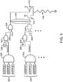
- Fig. 3 is a circuit diagram showing a portion of the drive circuit for the printhead of Fig. 1 .
- the drive circuit includes a circuit layer, which includes two transistors 110 and logic components for controlling the firing of the transistors 110.
- the output of each transistor 110 is coupled to a single resistor 108, which is used as the heating element for fluid ejection and is associated with a single nozzle 104 ( Fig. 1 ).
- the resistor 108 is part of the fluidic layer.
- the resistor 108 and transistors 110 are also shown in Fig. 1 .
- the components shown in Fig. 3 may be repeated for each pair of transistors 110 on the printhead.
- the drive circuit can include additional components not shown in Fig. 3 .
- the circuit layer of Fig. 3 is standardized, meaning that it can be used in combination with several different fluidic layer designs. The placement and number of resistors 108 will vary depending on the nozzle density of the printhead.
- three address bits 300 are received by AND gates 302. Three address bits are used in this example, because there are eight unique nozzle addresses for each primitive.
- the three address bits 300 are labeled ADDR[0], ADDR[1], and ADDR[2].
- An address bit label proceeded by the letter "n" indicates that the address bit has been inverted.
- Each unique combination of address bits 300 will cause the output of one of the AND gates 302 to output a logic one.
- the output of each AND gate 302 is referred to as the "address selection signal" and is a single digital logic bit that indicates which one of the nozzles in a primitive is selected for activation.
- each AND gate 302 is sent to another network of AND gates 304 along with the firing signal 306 and the primitive data 308.
- the output of each AND gate 304 can be coupled to the gate of one or both transistors 110, depending on the type of nozzle configuration. In the example shown in Fig. 3 , the output corresponding to address 0 is output to both of the transistors 110. By comparison, in an implementation with twice as many nozzles 104, one transistor 110 could be coupled to address 0 and the other transistor 110 could be coupled to address 1. Accordingly, it can be seen that the standardized drive circuit component layout of Fig. 3 can be used to support various fluidic layouts (different nozzle densities, for example) without any change in the semiconductor components.
- the interconnect layer provides the electrical connections between the semiconductor components and enables the standardized drive circuit component layout to be adapted to a variety of various fluidic layouts. For example, two different nozzle densities can be supported with minor changes in the interconnect layer as indicated by the circle 310, which shows that the output at address 1 is floating, while the output at address 0 is coupled to both transistors 110.
- Fig. 3 Various other changes can be made to the configuration shown in Fig. 3 .
- the logic components of Fig. 3 are shown as a set of AND gates.
- the logic components may be implemented as any suitable combination of electronic devices, such as AND gates, OR gates, inverters, flip-flops, and diodes, among others.
- various modifications can also be made to the interconnect layer.
- the output at address 0 could be coupled to one of the transistors 110, and the other transistor 110 could be left uncoupled to any output.
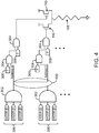
- Another technique for configuring the drive circuitry is shown in Fig. 4 .
- Fig. 4 is a circuit diagram showing another configuration of the drive circuit.
- the drive circuit of Fig. 4 shows another way of connecting the components of the circuit layer.
- the circuit layer and fluidic layer of Fig. 4 is the same as Fig. 3 .
- the drive circuitry is configured differently by using a different interconnect layout.
- each of the AND gates 304 is coupled to one of the transistors 110.
- each transistor 110 is triggered by a different set of logic components.
- the output of the AND gate 302 associated with address 0 is coupled to both networks of logic gates 304. This is indicated by the circle 400, which shows that the output at address 1 is floating, while the output at address 0 is coupled to the logic gates 304.
- the output of the AND gate 302 associated with address 0 can coupled to one network of logic gates 304, and the output of the AND gate 302 associated with address 1 can be coupled to the other networks of logic gates 304.
- Fig. 5 is a process flow diagram for a method of manufacturing a printhead.
- the method 500 can be performed using known semiconductor and MEMs fabrication techniques, which include material deposition, removal, patterning, electrical property modification, and the like.
- the drive circuit components of the circuit layer are formed.
- the drive circuit components may be formed in semiconductor such as silicon.
- the drive circuit components are the devices that are used to address and activate the energy delivery devices associated with particular nozzles.
- the layout of the drive circuit components is a standardized layout that is not dependent on a nozzle density of the printhead and can be used in different printhead types with different nozzle densities.
- the fluidic layer includes the fluid chamber with the fluid ejection nozzles, fluid feed channels, energy delivery devices, and the like.
- the fluidic layer is formed over the drive circuit components of the circuit layer.
- the term "over” does not mean "directly over.” Accordingly, forming the fluidic layer over the drive circuit components means that the fluidic layer can be formed directly over the drive circuit components, or additional intervening layers can be formed over the drive circuit components prior to forming the fluidic layer.
- an interconnect layer design is selected.
- the layout of the interconnect layer can be selected depending, at least in part, on the nozzle density of the printhead.
- the interconnect layer is formed over the drive circuit components of the circuit layer.
- the interconnect layer configures the drive circuit components by coupling the drive circuit components to one another and coupling the drive circuit components to the appropriate energy delivery devices according to the selected configuration.
- each available activation device in the circuit layer is paired with a nozzle, and each energy delivery device is coupled to a single activation device that is addressable to activate the nozzle.
- the forming of the interconnect layer may leave some of the drive circuit components permanently uncoupled from all of the activation devices and unpaired with a corresponding nozzle.
- each energy delivery device can be coupled to a pair of activation devices that are simultaneously addressable to activate the nozzle.
- the pair of activation devices may be driven by an output received from a same component of the drive circuitry, as shown in Fig. 3 for example.
- Each one of the pair of activation devices may also be driven by separate components of the drive circuitry, as shown in Fig. 4 for example.
- each energy delivery device is coupled to a single activation device, and the remaining half of the activation devices is permanently uncoupled.
- the process flow diagram of Fig. 5 is not intended to indicate that the operations of the method 500 are to be executed in any particular order, or that all of the operations of the method 500 are to be included in every case.
- the interconnect layer is formed over the drive circuit components before the fluidic devices are formed over the drive circuit components.
- the method 500 can include any suitable number of additional operations.
- Fig. 6 is a block diagram showing a simplified example of a printhead assembly that includes a standardized drive circuit component layout.
- the example printhead 600 includes a fluidic device 602 coupled to an energy delivery device 604 that can cause fluid to be ejected from a nozzle 606.
- the fluidic device 602 may include a fluid chamber, and the energy delivery device 604 may be a heating element such as a resistor.
- the printhead 600 also includes a circuit layer that includes drive circuit components.
- the drive circuit components include activation devices 608 to activate the energy delivery device 604 and drive logic 610 to drive the activation devices.
- each activation device 608 may be a transistor such as a FET, and the drive logic 610 may include a logic gate or a network of logic gates and other circuitry. Each activation device 608 is coupled to separate drive logic 610.
- the printhead also includes an interconnect layer to electrically couple the drive circuit components. The interconnect layer in the example printhead of Fig. 6 couples the same address selection signal 612 to the drive logic 610 coupled to both activation devices 608.
- Fig. 7 is a block diagram showing a simplified example of another printhead assembly that includes a standardized drive circuit component layout.
- the printhead includes a fluidic device 602, energy delivery device 604, nozzle 606, activation devices 608, drive logic 610, and an interconnect layer to electrically couple the drive circuit components.
- the interconnect layer in the example printhead 700 of Fig. 7 couples the same drive circuit component within the drive logic 610 to both of the activation devices 608.
- an additional drive logic may also be present in the printhead 700, but is permanently decoupled from any activation device and cannot activate a nozzle.
Landscapes
- Engineering & Computer Science (AREA)
- Microelectronics & Electronic Packaging (AREA)
- Particle Formation And Scattering Control In Inkjet Printers (AREA)
Claims (11)
- Verfahren (500) zur Herstellung eines Druckkopfes, Folgendes umfassend:Bilden von Ansteuerschaltungskomponenten (502), wobei eine Anordnung der Ansteuerschaltungskomponenten eine standardisierte Anordnung ist, die nicht von einer Düsendichte des Druckkopfes abhängig ist;Bilden von Fluidvorrichtungen (504) über den Ansteuerschaltungskomponenten, wobei die Fluidvorrichtungen Fluidkammern mit Fluidausstoßdüsen umfassen; undgekennzeichnet durch Folgendes:
Bilden einer Verbindungsschicht (508) über den Ansteuerschaltungskomponenten, wobei die Verbindungsschicht die Ansteuerschaltungskomponenten konfiguriert und wobei eine Anordnung der Verbindungsschicht, zumindest teilweise auf der Düsendichte des Druckkopfes basierend, ausgewählt ist (506). - Verfahren nach Anspruch 1, das ein Bilden einer Vielzahl von Energieabgabevorrichtungen (108) und einer Vielzahl von Aktivierungsvorrichtungen (110) umfasst, die die Energieabgabevorrichtungen (108) aktivieren, wobei jede der Fluidausstoßdüsen (104) einer entsprechenden Energieabgabevorrichtung (108) zugeordnet ist und wobei das Bilden der Verbindungsschicht ein Koppeln jeder Aktivierungsvorrichtung (110) mit einer Energieabgabevorrichtung (108) umfasst, die zum Aktivieren der Düse (104) angesteuert werden kann.
- Verfahren nach Anspruch 1, das ein Bilden einer Vielzahl von Energieabgabevorrichtungen (108) und einer Vielzahl von Aktivierungsvorrichtungen (110) zum Aktivieren der Energieabgabevorrichtungen (108) umfasst, wobei jede der Fluidausstoßdüsen (104) einer entsprechenden Energieabgabevorrichtung (108) zugeordnet ist und wobei das Bilden der Verbindungsschicht ein Koppeln jeder Energieabgabevorrichtung (108) mit einem Paar von Aktivierungsvorrichtungen (110) umfasst, die zum Aktivieren der Düse (104) angesteuert werden kann.
- Verfahren nach Anspruch 3, wobei das Paar von Aktivierungsvorrichtungen (110) über eine Ausgabe (304) gesteuert wird, die von derselben der Ansteuerschaltungskomponenten empfangen wird.
- Verfahren nach Anspruch 3, wobei das Paar von Aktivierungsvorrichtungen (110) eine erste Aktivierungsvorrichtung (608) umfasst, die über eine erste Ausgabe gesteuert wird, die von einer ersten der Ansteuerschaltungskomponenten (610) empfangen wird, sowie eine zweite Aktivierungsvorrichtung (608), die über eine zweite Ausgabe gesteuert wird, die von einer zweiten der Ansteuerschaltungskomponenten (610) empfangen wird.
- Das Verfahren nach Anspruch 1, bei dem das Bilden der Verbindungsschicht umfasst, dass einige der Ansteuerschaltungskomponenten von allen Aktivierungsvorrichtungen (110) dauerhaft entkoppelt bleiben.
- Verfahren nach Anspruch 1, das ein Bilden einer Vielzahl von Energieabgabevorrichtungen (108) und einer Vielzahl von Aktivierungsvorrichtungen (110) zum Aktivieren der Energieabgabevorrichtungen (108) umfasst, wobei jede der Fluidausstoßdüsen (104) einer entsprechenden Energieabgabevorrichtung (108) zugeordnet ist und wobei das Bilden der Verbindungsschicht ein Koppeln jeder Aktivierungsvorrichtung (110) mit einer einzelnen Energieabgabevorrichtung (108), die zum Aktivieren der Düse (104) angesteuert werden kann, und ein dauerhaftes Entkoppeln der Hälfte der Vielzahl von Aktivierungsvorrichtungen (110) umfasst.
- Verfahren nach Anspruch 1, das ein Speichern einer Kennung in einer Speichervorrichtung (210) des Druckkopfes (100) umfasst, wobei ein Drucker (202) die Kennung verwendet, um zu bestimmen, welche Düsenadressen (104) des Druckkopfes gültig sind.
- Verfahren nach Anspruch 1, wobei die Anordnung der Ansteuerschaltungskomponenten bei Druckköpfen mit unterschiedlicher Düsendichte verwendet werden kann.
- Ein Druckkopf (100, 600), umfassend:
eine Fluidvorrichtung (602), die mit einer Energieabgabevorrichtung (604) gekoppelt ist, um zu bewirken, dass Fluid aus einer Düse (606) ausgestoßen wird:
eine Schaltungsschicht, welche Ansteuerschaltungskomponenten umfasst, wobei die Ansteuerschaltungskomponenten Folgendes umfassen:eine erste und eine zweite Aktivierungsvorrichtung (608) zum Aktivieren der Energieversorgungsvorrichtung (604);eine erste Ansteuerlogik (610), die mit der ersten Aktivierungsvorrichtung (608) gekoppelt ist; undeine zweite Ansteuerlogik (610), die mit der zweiten Aktivierungsvorrichtung (608) gekoppelt ist;undeine Verbindungsschicht zum elektrischen Koppeln der Ansteuerschaltungskomponenten, wobei die Verbindungsschicht zum Koppeln desselben Adressauswahlsignals (612) mit der ersten Ansteuerlogik (610) und der zweiten Ansteuerlogik (610) ausgelegt ist,dadurch gekennzeichnet, dass:
die Verbindungsschicht über den Ansteuerschaltungskomponenten gebildet ist, um die Ansteuerschaltungskomponenten in einer Anordnung zu konfigurieren, die zumindest teilweise auf Basis der Düsendichte des Druckkopfes ausgewählt wird, so dass die Verbindungsschicht zusätzliche Ansteuerschaltungskomponenten beinhaltet, die unbenutzten Adressen zugeordnet sind und dauerhaft von der Aktivierung einer Düse (606) auf dem Druckkopf deaktiviert sind. - Druckkopf nach Anspruch 10, wobei der Druckkopf einen Speicher (210) beinhaltet, der eine Düsendichte des Druckkopfes identifiziert.
Applications Claiming Priority (1)
| Application Number | Priority Date | Filing Date | Title |
|---|---|---|---|
| PCT/US2014/068079 WO2016089372A1 (en) | 2014-12-02 | 2014-12-02 | Printhead |
Publications (3)
| Publication Number | Publication Date |
|---|---|
| EP3227121A1 EP3227121A1 (de) | 2017-10-11 |
| EP3227121A4 EP3227121A4 (de) | 2018-07-11 |
| EP3227121B1 true EP3227121B1 (de) | 2019-11-20 |
Family
ID=56092135
Family Applications (1)
| Application Number | Title | Priority Date | Filing Date |
|---|---|---|---|
| EP14907213.4A Not-in-force EP3227121B1 (de) | 2014-12-02 | 2014-12-02 | Druckkopf |
Country Status (4)
| Country | Link |
|---|---|
| US (2) | US10286653B2 (de) |
| EP (1) | EP3227121B1 (de) |
| CN (2) | CN109466178B (de) |
| WO (1) | WO2016089372A1 (de) |
Families Citing this family (7)
| Publication number | Priority date | Publication date | Assignee | Title |
|---|---|---|---|---|
| CN109466178B (zh) * | 2014-12-02 | 2020-07-17 | 惠普发展公司,有限责任合伙企业 | 打印头 |
| JP7134733B2 (ja) * | 2018-06-25 | 2022-09-12 | キヤノン株式会社 | 記録素子基板、液体吐出ヘッド、および液体吐出装置 |
| AU2019428181B2 (en) | 2019-02-06 | 2023-11-16 | Hewlett-Packard Development Company, L.P. | Data packets comprising random numbers for controlling fluid dispensing devices |
| PL4206896T3 (pl) | 2019-02-06 | 2024-10-28 | Hewlett-Packard Development Company L.P. | Identyfikacja bitów losowych w pakietach danych sterujących |
| AU2019428638B2 (en) | 2019-02-06 | 2023-11-09 | Hewlett-Packard Development Company, L.P. | Integrated circuit with address drivers for fluidic die |
| KR102685237B1 (ko) | 2019-02-06 | 2024-07-15 | 휴렛-팩커드 디벨롭먼트 컴퍼니, 엘.피. | 간헐적 클럭 신호를 사용하는 메모리 어레이를 갖는 프린트 컴포넌트 |
| US12257837B2 (en) | 2020-10-23 | 2025-03-25 | Hewlett-Packard Development Company, L.P. | Interspersed fluidic elements and circuit elements in a fluidic die |
Family Cites Families (18)
| Publication number | Priority date | Publication date | Assignee | Title |
|---|---|---|---|---|
| CA2075097C (en) | 1991-08-02 | 2000-03-28 | Hiroyuki Ishinaga | Recording apparatus, recording head and substrate therefor |
| JP3200098B2 (ja) | 1991-08-02 | 2001-08-20 | キヤノン株式会社 | インクジェット記録ヘッドおよびインクジェット記録装置 |
| EP1563998B8 (de) | 1996-06-26 | 2010-10-20 | Canon Kabushiki Kaisha | Aufzeichnungskopf und Aufzeichnungsapparat unter Verwendung desselben |
| US6318846B1 (en) * | 1999-08-30 | 2001-11-20 | Hewlett-Packard Company | Redundant input signal paths for an inkjet print head |
| JP3693118B2 (ja) | 2002-08-12 | 2005-09-07 | セイコーエプソン株式会社 | シリコンデバイスの製造方法及び液体噴射ヘッドの製造方法並びに液体噴射ヘッド |
| JP4593905B2 (ja) | 2003-06-30 | 2010-12-08 | 京セラ株式会社 | 圧電アクチュエータおよびその製造方法、並びに液体吐出装置 |
| US7018012B2 (en) | 2003-11-14 | 2006-03-28 | Lexmark International, Inc. | Microfluid ejection device having efficient logic and driver circuitry |
| TWI225009B (en) * | 2003-12-26 | 2004-12-11 | Ind Tech Res Inst | Printing apparatus, ink jetting head, ink jetting head driving control circuit and method for controlling same |
| US7195341B2 (en) * | 2004-09-30 | 2007-03-27 | Lexmark International, Inc. | Power and ground buss layout for reduced substrate size |
| KR100666955B1 (ko) | 2004-11-15 | 2007-01-10 | 삼성전자주식회사 | 잉크젯 프린트 헤드 및 그 제조 방법 |
| US9283750B2 (en) * | 2005-05-20 | 2016-03-15 | Hewlett-Packard Development Company, L.P. | Constant current mode firing circuit for thermal inkjet-printing nozzle |
| JP4764690B2 (ja) * | 2005-09-27 | 2011-09-07 | 富士フイルム株式会社 | 画像形成装置 |
| JP2007097280A (ja) | 2005-09-28 | 2007-04-12 | Kyocera Corp | 圧電アクチュエータおよびその製造方法、並びにインクジェット記録ヘッド |
| CN101062610A (zh) * | 2006-04-26 | 2007-10-31 | 国际联合科技股份有限公司 | 喷墨印头控制电路 |
| EP2474421A1 (de) | 2009-08-31 | 2012-07-11 | Mimaki Engineering Co., Ltd. | Tintenstrahldrucker und druckverfahren |
| US8485623B2 (en) | 2010-10-01 | 2013-07-16 | Zamtec Ltd | Pagewidth inkjet printhead configured such that printed dot density exceeds nozzle density |
| WO2013055356A1 (en) | 2011-10-14 | 2013-04-18 | Hewlett-Packard Development Company, L.P. | Firing actuator power supply system |
| CN109466178B (zh) | 2014-12-02 | 2020-07-17 | 惠普发展公司,有限责任合伙企业 | 打印头 |
-
2014
- 2014-12-02 CN CN201811309686.7A patent/CN109466178B/zh not_active Expired - Fee Related
- 2014-12-02 WO PCT/US2014/068079 patent/WO2016089372A1/en not_active Ceased
- 2014-12-02 EP EP14907213.4A patent/EP3227121B1/de not_active Not-in-force
- 2014-12-02 US US15/526,921 patent/US10286653B2/en active Active
- 2014-12-02 CN CN201480083842.6A patent/CN107000440B/zh not_active Expired - Fee Related
-
2019
- 2019-05-01 US US16/400,071 patent/US10960661B2/en not_active Expired - Fee Related
Non-Patent Citations (1)
| Title |
|---|
| None * |
Also Published As
| Publication number | Publication date |
|---|---|
| EP3227121A1 (de) | 2017-10-11 |
| CN107000440A (zh) | 2017-08-01 |
| CN109466178A (zh) | 2019-03-15 |
| US10286653B2 (en) | 2019-05-14 |
| US20170320320A1 (en) | 2017-11-09 |
| EP3227121A4 (de) | 2018-07-11 |
| CN107000440B (zh) | 2018-11-06 |
| US10960661B2 (en) | 2021-03-30 |
| CN109466178B (zh) | 2020-07-17 |
| WO2016089372A1 (en) | 2016-06-09 |
| US20190255842A1 (en) | 2019-08-22 |
Similar Documents
| Publication | Publication Date | Title |
|---|---|---|
| US10960661B2 (en) | Fluid ejection device circuit | |
| US11123981B2 (en) | Printhead nozzle addressing | |
| KR100920300B1 (ko) | 잉크젯 프린트헤드 | |
| KR100429352B1 (ko) | 프린터, 액체 방출 장치, 프린트 카트리지, 프린팅 시스템, 및 프린트 헤드 제조 방법 | |
| KR100871542B1 (ko) | 잉크젯 프린트헤드 및 그 작동 방법 | |
| JP4402880B2 (ja) | インクを噴出させるための方法および装置 | |
| CN107073954B (zh) | 打印头组件及打印的方法 | |
| AU2002227165A1 (en) | Inkjet printhead and method for the same | |
| JP4532890B2 (ja) | 記録ヘッドおよび該記録ヘッドを備えた記録装置 | |
| WO2006105373A2 (en) | Power distribution routing to reduce chip area | |
| JP2010505657A (ja) | 3端子切り換え素子を有するアレイ・プリントヘッド |
Legal Events
| Date | Code | Title | Description |
|---|---|---|---|
| STAA | Information on the status of an ep patent application or granted ep patent |
Free format text: STATUS: THE INTERNATIONAL PUBLICATION HAS BEEN MADE |
|
| PUAI | Public reference made under article 153(3) epc to a published international application that has entered the european phase |
Free format text: ORIGINAL CODE: 0009012 |
|
| STAA | Information on the status of an ep patent application or granted ep patent |
Free format text: STATUS: REQUEST FOR EXAMINATION WAS MADE |
|
| 17P | Request for examination filed |
Effective date: 20170522 |
|
| AK | Designated contracting states |
Kind code of ref document: A1 Designated state(s): AL AT BE BG CH CY CZ DE DK EE ES FI FR GB GR HR HU IE IS IT LI LT LU LV MC MK MT NL NO PL PT RO RS SE SI SK SM TR |
|
| AX | Request for extension of the european patent |
Extension state: BA ME |
|
| DAX | Request for extension of the european patent (deleted) | ||
| A4 | Supplementary search report drawn up and despatched |
Effective date: 20180612 |
|
| RIC1 | Information provided on ipc code assigned before grant |
Ipc: B41J 2/175 20060101AFI20180606BHEP Ipc: B41J 2/045 20060101ALI20180606BHEP Ipc: B41J 2/135 20060101ALI20180606BHEP |
|
| RAP1 | Party data changed (applicant data changed or rights of an application transferred) |
Owner name: HEWLETT-PACKARD DEVELOPMENT COMPANY, L.P. |
|
| REG | Reference to a national code |
Ref country code: DE Ref legal event code: R079 Ref document number: 602014057335 Country of ref document: DE Free format text: PREVIOUS MAIN CLASS: B41J0002175000 Ipc: B41J0002070000 |
|
| GRAP | Despatch of communication of intention to grant a patent |
Free format text: ORIGINAL CODE: EPIDOSNIGR1 |
|
| STAA | Information on the status of an ep patent application or granted ep patent |
Free format text: STATUS: GRANT OF PATENT IS INTENDED |
|
| RIC1 | Information provided on ipc code assigned before grant |
Ipc: B41J 2/135 20060101ALI20190521BHEP Ipc: B41J 2/175 20060101ALI20190521BHEP Ipc: B41J 2/045 20060101ALI20190521BHEP Ipc: B41J 2/07 20060101AFI20190521BHEP |
|
| INTG | Intention to grant announced |
Effective date: 20190612 |
|
| GRAS | Grant fee paid |
Free format text: ORIGINAL CODE: EPIDOSNIGR3 |
|
| GRAA | (expected) grant |
Free format text: ORIGINAL CODE: 0009210 |
|
| STAA | Information on the status of an ep patent application or granted ep patent |
Free format text: STATUS: THE PATENT HAS BEEN GRANTED |
|
| AK | Designated contracting states |
Kind code of ref document: B1 Designated state(s): AL AT BE BG CH CY CZ DE DK EE ES FI FR GB GR HR HU IE IS IT LI LT LU LV MC MK MT NL NO PL PT RO RS SE SI SK SM TR |
|
| REG | Reference to a national code |
Ref country code: GB Ref legal event code: FG4D |
|
| REG | Reference to a national code |
Ref country code: CH Ref legal event code: EP |
|
| REG | Reference to a national code |
Ref country code: DE Ref legal event code: R096 Ref document number: 602014057335 Country of ref document: DE |
|
| REG | Reference to a national code |
Ref country code: IE Ref legal event code: FG4D |
|
| REG | Reference to a national code |
Ref country code: AT Ref legal event code: REF Ref document number: 1203744 Country of ref document: AT Kind code of ref document: T Effective date: 20191215 |
|
| REG | Reference to a national code |
Ref country code: NL Ref legal event code: MP Effective date: 20191120 |
|
| REG | Reference to a national code |
Ref country code: LT Ref legal event code: MG4D |
|
| PG25 | Lapsed in a contracting state [announced via postgrant information from national office to epo] |
Ref country code: SE Free format text: LAPSE BECAUSE OF FAILURE TO SUBMIT A TRANSLATION OF THE DESCRIPTION OR TO PAY THE FEE WITHIN THE PRESCRIBED TIME-LIMIT Effective date: 20191120 Ref country code: LV Free format text: LAPSE BECAUSE OF FAILURE TO SUBMIT A TRANSLATION OF THE DESCRIPTION OR TO PAY THE FEE WITHIN THE PRESCRIBED TIME-LIMIT Effective date: 20191120 Ref country code: NL Free format text: LAPSE BECAUSE OF FAILURE TO SUBMIT A TRANSLATION OF THE DESCRIPTION OR TO PAY THE FEE WITHIN THE PRESCRIBED TIME-LIMIT Effective date: 20191120 Ref country code: LT Free format text: LAPSE BECAUSE OF FAILURE TO SUBMIT A TRANSLATION OF THE DESCRIPTION OR TO PAY THE FEE WITHIN THE PRESCRIBED TIME-LIMIT Effective date: 20191120 Ref country code: GR Free format text: LAPSE BECAUSE OF FAILURE TO SUBMIT A TRANSLATION OF THE DESCRIPTION OR TO PAY THE FEE WITHIN THE PRESCRIBED TIME-LIMIT Effective date: 20200221 Ref country code: NO Free format text: LAPSE BECAUSE OF FAILURE TO SUBMIT A TRANSLATION OF THE DESCRIPTION OR TO PAY THE FEE WITHIN THE PRESCRIBED TIME-LIMIT Effective date: 20200220 Ref country code: FI Free format text: LAPSE BECAUSE OF FAILURE TO SUBMIT A TRANSLATION OF THE DESCRIPTION OR TO PAY THE FEE WITHIN THE PRESCRIBED TIME-LIMIT Effective date: 20191120 Ref country code: BG Free format text: LAPSE BECAUSE OF FAILURE TO SUBMIT A TRANSLATION OF THE DESCRIPTION OR TO PAY THE FEE WITHIN THE PRESCRIBED TIME-LIMIT Effective date: 20200220 |
|
| PG25 | Lapsed in a contracting state [announced via postgrant information from national office to epo] |
Ref country code: RS Free format text: LAPSE BECAUSE OF FAILURE TO SUBMIT A TRANSLATION OF THE DESCRIPTION OR TO PAY THE FEE WITHIN THE PRESCRIBED TIME-LIMIT Effective date: 20191120 Ref country code: HR Free format text: LAPSE BECAUSE OF FAILURE TO SUBMIT A TRANSLATION OF THE DESCRIPTION OR TO PAY THE FEE WITHIN THE PRESCRIBED TIME-LIMIT Effective date: 20191120 Ref country code: IS Free format text: LAPSE BECAUSE OF FAILURE TO SUBMIT A TRANSLATION OF THE DESCRIPTION OR TO PAY THE FEE WITHIN THE PRESCRIBED TIME-LIMIT Effective date: 20200320 |
|
| PG25 | Lapsed in a contracting state [announced via postgrant information from national office to epo] |
Ref country code: AL Free format text: LAPSE BECAUSE OF FAILURE TO SUBMIT A TRANSLATION OF THE DESCRIPTION OR TO PAY THE FEE WITHIN THE PRESCRIBED TIME-LIMIT Effective date: 20191120 |
|
| PG25 | Lapsed in a contracting state [announced via postgrant information from national office to epo] |
Ref country code: RO Free format text: LAPSE BECAUSE OF FAILURE TO SUBMIT A TRANSLATION OF THE DESCRIPTION OR TO PAY THE FEE WITHIN THE PRESCRIBED TIME-LIMIT Effective date: 20191120 Ref country code: CZ Free format text: LAPSE BECAUSE OF FAILURE TO SUBMIT A TRANSLATION OF THE DESCRIPTION OR TO PAY THE FEE WITHIN THE PRESCRIBED TIME-LIMIT Effective date: 20191120 Ref country code: PT Free format text: LAPSE BECAUSE OF FAILURE TO SUBMIT A TRANSLATION OF THE DESCRIPTION OR TO PAY THE FEE WITHIN THE PRESCRIBED TIME-LIMIT Effective date: 20200412 Ref country code: EE Free format text: LAPSE BECAUSE OF FAILURE TO SUBMIT A TRANSLATION OF THE DESCRIPTION OR TO PAY THE FEE WITHIN THE PRESCRIBED TIME-LIMIT Effective date: 20191120 Ref country code: DK Free format text: LAPSE BECAUSE OF FAILURE TO SUBMIT A TRANSLATION OF THE DESCRIPTION OR TO PAY THE FEE WITHIN THE PRESCRIBED TIME-LIMIT Effective date: 20191120 |
|
| REG | Reference to a national code |
Ref country code: CH Ref legal event code: PL |
|
| REG | Reference to a national code |
Ref country code: AT Ref legal event code: MK05 Ref document number: 1203744 Country of ref document: AT Kind code of ref document: T Effective date: 20191120 |
|
| REG | Reference to a national code |
Ref country code: DE Ref legal event code: R097 Ref document number: 602014057335 Country of ref document: DE |
|
| REG | Reference to a national code |
Ref country code: BE Ref legal event code: MM Effective date: 20191231 |
|
| PG25 | Lapsed in a contracting state [announced via postgrant information from national office to epo] |
Ref country code: SK Free format text: LAPSE BECAUSE OF FAILURE TO SUBMIT A TRANSLATION OF THE DESCRIPTION OR TO PAY THE FEE WITHIN THE PRESCRIBED TIME-LIMIT Effective date: 20191120 Ref country code: SM Free format text: LAPSE BECAUSE OF FAILURE TO SUBMIT A TRANSLATION OF THE DESCRIPTION OR TO PAY THE FEE WITHIN THE PRESCRIBED TIME-LIMIT Effective date: 20191120 Ref country code: MC Free format text: LAPSE BECAUSE OF FAILURE TO SUBMIT A TRANSLATION OF THE DESCRIPTION OR TO PAY THE FEE WITHIN THE PRESCRIBED TIME-LIMIT Effective date: 20191120 |
|
| PLBE | No opposition filed within time limit |
Free format text: ORIGINAL CODE: 0009261 |
|
| STAA | Information on the status of an ep patent application or granted ep patent |
Free format text: STATUS: NO OPPOSITION FILED WITHIN TIME LIMIT |
|
| 26N | No opposition filed |
Effective date: 20200821 |
|
| PG25 | Lapsed in a contracting state [announced via postgrant information from national office to epo] |
Ref country code: ES Free format text: LAPSE BECAUSE OF FAILURE TO SUBMIT A TRANSLATION OF THE DESCRIPTION OR TO PAY THE FEE WITHIN THE PRESCRIBED TIME-LIMIT Effective date: 20191120 Ref country code: IE Free format text: LAPSE BECAUSE OF NON-PAYMENT OF DUE FEES Effective date: 20191202 Ref country code: LU Free format text: LAPSE BECAUSE OF NON-PAYMENT OF DUE FEES Effective date: 20191202 |
|
| PG25 | Lapsed in a contracting state [announced via postgrant information from national office to epo] |
Ref country code: LI Free format text: LAPSE BECAUSE OF NON-PAYMENT OF DUE FEES Effective date: 20191231 Ref country code: CH Free format text: LAPSE BECAUSE OF NON-PAYMENT OF DUE FEES Effective date: 20191231 Ref country code: PL Free format text: LAPSE BECAUSE OF FAILURE TO SUBMIT A TRANSLATION OF THE DESCRIPTION OR TO PAY THE FEE WITHIN THE PRESCRIBED TIME-LIMIT Effective date: 20191120 Ref country code: AT Free format text: LAPSE BECAUSE OF FAILURE TO SUBMIT A TRANSLATION OF THE DESCRIPTION OR TO PAY THE FEE WITHIN THE PRESCRIBED TIME-LIMIT Effective date: 20191120 Ref country code: SI Free format text: LAPSE BECAUSE OF FAILURE TO SUBMIT A TRANSLATION OF THE DESCRIPTION OR TO PAY THE FEE WITHIN THE PRESCRIBED TIME-LIMIT Effective date: 20191120 Ref country code: BE Free format text: LAPSE BECAUSE OF NON-PAYMENT OF DUE FEES Effective date: 20191231 |
|
| PG25 | Lapsed in a contracting state [announced via postgrant information from national office to epo] |
Ref country code: IT Free format text: LAPSE BECAUSE OF FAILURE TO SUBMIT A TRANSLATION OF THE DESCRIPTION OR TO PAY THE FEE WITHIN THE PRESCRIBED TIME-LIMIT Effective date: 20191120 |
|
| PG25 | Lapsed in a contracting state [announced via postgrant information from national office to epo] |
Ref country code: CY Free format text: LAPSE BECAUSE OF FAILURE TO SUBMIT A TRANSLATION OF THE DESCRIPTION OR TO PAY THE FEE WITHIN THE PRESCRIBED TIME-LIMIT Effective date: 20191120 |
|
| PG25 | Lapsed in a contracting state [announced via postgrant information from national office to epo] |
Ref country code: HU Free format text: LAPSE BECAUSE OF FAILURE TO SUBMIT A TRANSLATION OF THE DESCRIPTION OR TO PAY THE FEE WITHIN THE PRESCRIBED TIME-LIMIT; INVALID AB INITIO Effective date: 20141202 Ref country code: MT Free format text: LAPSE BECAUSE OF FAILURE TO SUBMIT A TRANSLATION OF THE DESCRIPTION OR TO PAY THE FEE WITHIN THE PRESCRIBED TIME-LIMIT Effective date: 20191120 |
|
| PGFP | Annual fee paid to national office [announced via postgrant information from national office to epo] |
Ref country code: GB Payment date: 20211118 Year of fee payment: 8 Ref country code: FR Payment date: 20211117 Year of fee payment: 8 |
|
| PG25 | Lapsed in a contracting state [announced via postgrant information from national office to epo] |
Ref country code: TR Free format text: LAPSE BECAUSE OF FAILURE TO SUBMIT A TRANSLATION OF THE DESCRIPTION OR TO PAY THE FEE WITHIN THE PRESCRIBED TIME-LIMIT Effective date: 20191120 |
|
| PG25 | Lapsed in a contracting state [announced via postgrant information from national office to epo] |
Ref country code: MK Free format text: LAPSE BECAUSE OF FAILURE TO SUBMIT A TRANSLATION OF THE DESCRIPTION OR TO PAY THE FEE WITHIN THE PRESCRIBED TIME-LIMIT Effective date: 20191120 |
|
| PGFP | Annual fee paid to national office [announced via postgrant information from national office to epo] |
Ref country code: DE Payment date: 20220616 Year of fee payment: 9 |
|
| GBPC | Gb: european patent ceased through non-payment of renewal fee |
Effective date: 20221202 |
|
| PG25 | Lapsed in a contracting state [announced via postgrant information from national office to epo] |
Ref country code: GB Free format text: LAPSE BECAUSE OF NON-PAYMENT OF DUE FEES Effective date: 20221202 |
|
| PG25 | Lapsed in a contracting state [announced via postgrant information from national office to epo] |
Ref country code: FR Free format text: LAPSE BECAUSE OF NON-PAYMENT OF DUE FEES Effective date: 20221231 |
|
| REG | Reference to a national code |
Ref country code: DE Ref legal event code: R119 Ref document number: 602014057335 Country of ref document: DE |
|
| PG25 | Lapsed in a contracting state [announced via postgrant information from national office to epo] |
Ref country code: DE Free format text: LAPSE BECAUSE OF NON-PAYMENT OF DUE FEES Effective date: 20240702 |
|
| PG25 | Lapsed in a contracting state [announced via postgrant information from national office to epo] |
Ref country code: DE Free format text: LAPSE BECAUSE OF NON-PAYMENT OF DUE FEES Effective date: 20240702 |