EP3228015B1 - Reduzierer von übertragungsrauschen - Google Patents
Reduzierer von übertragungsrauschen Download PDFInfo
- Publication number
- EP3228015B1 EP3228015B1 EP15868676.6A EP15868676A EP3228015B1 EP 3228015 B1 EP3228015 B1 EP 3228015B1 EP 15868676 A EP15868676 A EP 15868676A EP 3228015 B1 EP3228015 B1 EP 3228015B1
- Authority
- EP
- European Patent Office
- Prior art keywords
- sne
- input
- output
- additional
- signal
- Prior art date
- Legal status (The legal status is an assumption and is not a legal conclusion. Google has not performed a legal analysis and makes no representation as to the accuracy of the status listed.)
- Active
Links
Images


Classifications
-
- H—ELECTRICITY
- H04—ELECTRIC COMMUNICATION TECHNIQUE
- H04B—TRANSMISSION
- H04B1/00—Details of transmission systems, not covered by a single one of groups H04B3/00 - H04B13/00; Details of transmission systems not characterised by the medium used for transmission
- H04B1/02—Transmitters
- H04B1/04—Circuits
- H04B1/0475—Circuits with means for limiting noise, interference or distortion
-
- H—ELECTRICITY
- H03—ELECTRONIC CIRCUITRY
- H03H—IMPEDANCE NETWORKS, e.g. RESONANT CIRCUITS; RESONATORS
- H03H2/00—Networks using elements or techniques not provided for in groups H03H3/00 - H03H21/00
- H03H2/001—Networks using elements or techniques not provided for in groups H03H3/00 - H03H21/00 comprising magnetostatic wave network elements
Definitions
- One or more aspects of embodiments according to the present invention relate to transmitting circuits, and more particularly to a system for transmitting a signal with reduced noise.
- Radio frequency (RF) or microwave signals are on occasion deployed near each other with carrier frequencies that are offset by small frequency differences.
- RF radio frequency
- Such interference may degrade the signal to noise ratio in a system receiving one of the modulated carriers, or, if it is of sufficiently large magnitude, drive the receive system into compression.
- US Patent No. 4,488,122 discloses a device comprising a microstrip including a narrow conductor connected in series between a circuit input terminal and the power amplifier, a film of ferrimag-netic material positioned adjacent the conductor and magnetic biasing means.
- the biasing means normally biases the ferrimagnetic material to operate at frequen-cies about a selected center frequency for nonlinearly enhancing RF input signals as a function of input ampli-tude.
- the device normally, undesirably provides non-linear phase shifts to the input signal as a function of input power at frequencies removed from the center frequency.
- the device can be adjusted to produce phase shift which changes as a function of input power to offset the nonlinear phase shift of the RF amplifier.
- the output of the second SNE is connected to a transmitting antenna.
- the magnetic component includes a thin film of yttrium iron garnet (YIG) on a gadolinium gallium garnet (GGG) substrate.
- YIG yttrium iron garnet
- GGG gadolinium gallium garnet
- the thin film of YIG is a single crystal of YIG
- the GGG substrate is a single crystal of GGG
- the thin film of YIG is lattice-matched to the GGG substrate.
- a portion of the transmission line in proximity with the magnetic component follows a substantially straight path.
- the one or more magnets include two magnets, positioned and oriented with respect to the portion of the microwave transmission line so as to produce, in the magnetic component, a biasing magnetic field substantially parallel to the portion of the microwave transmission line.
- the transmit system includes a plurality of additional components connected in cascade to form a chain having an input and an output, the output of the first SNE connected to the input of the chain, the plurality of additional components including one or more additional SNEs and one or more additional amplifiers, the additional SNEs and the additional amplifiers alternating in the chain, each additional SNE of the one or more additional SNEs having an input and an output, each additional SNE of the one or more additional SNEs including: a microwave transmission line connected between the input and the output of the additional SNE; a magnetic component capable of supporting magnetostatic waves; the magnetic component secured in proximity to the microwave transmission line; one or more magnets secured in proximity to the magnetic component; each additional SNE of the one or more additional SNEs having the characteristic of allowing a signal to propagate from the input of the additional SNE to the output of the additional SNE: with a first attenuation when the power of the signal at the input of the SNE is less than a first threshold, and with a second attenuation when
- the chain includes, as a final element, an amplifier of the one or more additional amplifiers.
- the chain includes, as a final element, an SNE of the one or more additional SNEs.
- the output of the chain is connected to a transmitting antenna.
- the transmit system includes a digital-to-analog converter (DAC) having a digital input and an analog output, the output of the DAC being connected to the input of the first amplifier.
- DAC digital-to-analog converter
- filters attenuate signals in adjacent Nyquist zones, decreasing the out-of-band spurious signals associated with the data conversion process.
- a combination of a DAC, a Nyquist select filter, a driver amp, a mixer, a filter on the output of the mixer, and a high power amplifier may be connected in cascade. While the Nyquist select fixed filter attenuates noise and spurious signals outside of the operational band of the DAC, broadband noise (from both thermal and quantization sources) within the operational band of the DAC may be fed through the transmit chain. This noise is then amplified by the driver amp, and any remaining broadband noise after the post-mixer filter is also amplified by the high power amplifier.
- each element may be driven by its own DAC (with the transmit chain featuring several copies of the cascade described above), or a single DAC may be used to drive multiple elements.
- an N-way splitter may be used to distribute the transmit signal to N modules that apply independent amplitude and phase weights to each signal before amplification in a high power amplifier at every element.
- the broadband noise of the DAC is amplified by the amplifiers in the common transmit chain, and again by each high power amplifier at every element.
- some noise sources such as those associated with the common chain (including the DAC, if a single DAC is used), may be coherent, and thus add constructively to increase the total transmitted noise.
- Transmit noise causes several problems.
- One such problem is electromagnetic interference with separate systems that are either co-located with or sufficiently close to the noisy transmitter. Even if the separate system is operating in a different frequency band, the transmitted noise can be sufficient to raise the effective noise floor of the receive chain, or possibly drive the receive system into compression.
- Cancellation approaches may be used to suppress some interference. For example, a direct sample of the transmitted signal may be fed back into the receive chain with appropriate amplitude and time delay weights to cancel the signal returned from the aperture, or a cancellation signal may be generated through another DAC in an attempt to match the interfering signal. In each case, information about, or a sample of, the transmitted signal is needed; this may be impractical in geographically separated transmit-receive systems, such as cellular communication towers. Moreover, these approaches are not effective at reducing the broadband noise associated with the transmit chain.
- the signal to noise enhancer is a nonlinear passive device that attenuates signals below a first threshold power while passing signals above a second threshold power.
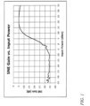
- FIG. 1 shows the gain of an SNE as a function of input power, when the input contains a single tone within the operating frequency range of the SNE.
- the transmission loss remains greater than 32 dB (i.e., the gain remains less than -32 dB).
- the loss decreases (i.e., the gain increases) to reach a loss of approximately 8 dB at a second threshold power of 12 dBm.
- the SNE provides high attenuation for signals with power below the first threshold power and low attenuation for signals with power above the second threshold power, the difference, in this example, being approximately 24 dB.
- the characteristics of an SNE may vary according to the details of its design, so that an SNE may exhibit, for example, less loss for a high-power tone, and the difference in attenuation between a high-power tone and a low-power tone (which also depends on how the first and second power thresholds are chosen) may be greater or less than the 24 dB of this example.
- an SNE with a difference in attenuation (between a high power tone and a low power tone) of as little as 5 dB may provide useful performance benefits.
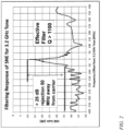
- a key feature of the SNE is the frequency selective nature of the high-power passband: low power signals close in frequency to the passed high-power signals are subject to high levels of attenuation.
- the principal tone is attenuated by 10 dB or less and signals at other frequencies that are 50 MHz or more from the principal tone are attenuated by at least 25 dB more than the amount by which the principal tone is attenuated.
- a conventional linear filter would need a quality factor (Q) of over 1000.
- the SNE acts as a high-Q (>1000) notch filter that automatically tunes to pass high power signals while rejecting low power signals in adjacent frequency bands.
- the characteristic of FIG. 2 corresponds to a measurement in which a low-power test tone was swept in frequency over a first range of frequencies extending below the frequency of the principal tone, and over a second range of frequencies extending above the frequency of the principal tone. Measurements of the attenuation of a test tone very near in frequency to the principal tone are challenging because of the large amplitude difference between the test tone and the principal tone; the characteristic of FIG. 2 thus excludes measurements of the attenuation (expected to be less than the minimum 10 dB attenuation shown) over a small frequency interval including the principal tone.
- the SNE is built according to the disclosure in U.S. Patent 4,283,692 (the "'692 Patent”).
- FIG. 3 is a photograph of a prototype SNE.
- a thin film of yttrium iron garnet (YIG) epitaxially grown on a gadolinium gallium garnet (GGG) substrate 105 is secured, with the thin film side down, on or immediately above a straight portion of a microstrip transmission line fabricated on a surface of a dielectric substrate 110.
- a DC bias magnetic field is applied to the YIG sample in a direction parallel to the straight portion of the microstrip transmission line by two magnets 115.
- Each magnet may be a permanent magnet, as shown in FIG.
- the thin film of YIG and the GGG substrate may each be a single crystal, and the thin film of YIG may be lattice-matched to the GGG substrate.
- the positions of the magnets are adjustable using translation stages 120; in a production unit the magnets may be installed in fixed positions identified, using the prototype, by adjusting the magnet positions in the prototype for acceptable performance.
- a single magnet may be used instead of a pair of magnets, or more than two magnets may be used.
- the propagation of electromagnetic signals along the transmission line excites magnetostatic waves (MSW) in the YIG film of the SNE; the MSW are long wavelength spin waves which may propagate at microwave frequencies in ferromagnetic materials placed within a biasing magnetic field. Microwave energy is coupled from the transmission line to MSW that propagate away from the transmission line.
- MSW magnetostatic waves
- the edge of the film may be ground at an angle, e.g., forming a bevel on the lower edges of the GGG substrate and YIG film, or the GGG substrate may be formed as a curved surface (e.g., the GGG substrate and YIG film may be in the shape of a circular disk).
- the MSW may be attenuated using a conductive material, such as a 0.6 nm layer of aluminum, deposited onto the surface of the microstrip dielectric substrate, sufficiently far from the transmission line to avoid significantly affecting modes propagating in the transmission line.
- the coupling of energy from waves travelling in the microstrip transmission line into magnetostatic surface waves may be increased by depositing a metal (e.g., gold) film on the YIG film in a pattern forming a slot parallel to the microstrip transmission line, or a coplanar structure with a central conductor parallel to the microstrip transmission line, between two coplanar ground planes.
- a metal e.g., gold
- magnetostatic surface waves are launched and propagated in the YIG film in response to an input signal applied to the microstrip transmission line.
- Magnetostatic volume waves are also possible with different directions of the magnetizing field relative to the YIG film, as is well known to those skilled in the art.
- Magnetostatic surface waves and magnetostatic volume waves are collectively referred to herein as magnetostatic waves (MSW).
- MSW magnetostatic waves
- the amount of energy that can be coupled from the transmission line to MSW is limited. Therefore, above a certain power level of the exciting signal, saturation occurs and no additional power can be coupled to MSW. As a result, for low signal power levels, the microwave energy is coupled from the transmission line to MSW. In contrast, for high signal power levels, the coupling to MSW saturates and the amount of loss imparted on the signal propagating from the input to the output of the SNE is reduced. This behavior gives rise to a significant enhancement of the signal-to-noise ratio when the noise power is less than the first threshold power of the SNE and the signal is a tone with power greater than the second threshold power of the SNE.
- a DAC 400 is followed by a fixed Nyquist select filter 402, by an amplifier 405 and by a first SNE 410, and optionally by additional amplifiers 405 and SNEs 410.
- the DAC may be followed by the Nyquist select filter 402 and then by an amplifier to boost the power of the principal tone in the signal to above the second threshold power, so that the principal tone will not be too greatly attenuated by the SNE 410; the gain of the amplifier may be selected, for example, so that the power at the input to the SNE 410 is within the design input power range of the SNE 410, e.g., 15-25 dBm.
- an SNE may have a design input power range with a significantly higher upper limit.
- the chain of components ends at the output of the first SNE 410, i.e., the output of the SNE 410 is the output of the circuit, which may, for example, be connected to a radiating or "transmitting" antenna.
- additional pairs of amplifiers 405 and SNEs 410 are added, each pair providing additional gain.
- FIG. 4B shows an example of such an embodiment, in which an amplifier 405 and an SNE 410 have been added to the transmit system of FIG. 4A .
- the 4B with an SNE 410 after the final amplifier 405 in the chain may be suitable for applications where the degradation in efficiency (i.e., the loss of the SNE for the principal tone, which may be 2-4 dB) is outweighed by the desire to achieve the lowest transmit noise power.
- the degradation in efficiency i.e., the loss of the SNE for the principal tone, which may be 2-4 dB
- Each SNE 410 improves the signal to noise ratio but it also attenuates the principal tone; in applications in which high output power is of greater value than high signal-to-noise ratio at the output, it may be advantageous to employ an amplifier, which may be a high power amplifier 415 as the final element in the chain, as illustrated in FIG. 4C .
- the final amplifier 415 is not followed by an SNE and is therefore not constrained to produce an output power within the design input power range of the SNE 410. In particular it may produce significantly higher power, e.g., 10 W, 100 W, or 1,000 W or more.
- a first SNE 410 is used after the DAC 400 (after the fixed Nyquist select filter 402) to provide an immediate improvement in the DAC's signal to noise ratio.
- the signal at the output of the first SNE 410 is then split by a first splitter 510 into several paths, or "first branches" (25 in the embodiment of FIG. 5 ), each corresponding to a subarray of the array antenna.
- the signal in each first branch is amplified to overcome power lost during the split, and sent through another SNE 410 to provide an additional improvement to the transmit signal to noise ratio.
- the signal in each of the first branches is then split again, by a plurality of second splitters 520, into several paths, or "second branches" (200 paths per subarray in the embodiment of FIG. 5 ), where individual amplitude and phase weights are applied with a multifunction circuit (MFC) 530, and the signal is amplified again before passing through another SNE for still more improvement in the transmit signal to noise ratio.
- the signal in each second branch is finally amplified by a high power amplifier 415.
- the signal path from the output of the first SNE 410 has a tree structure, the tree having a single input (connected to the output of the first SNE 410), the signal at the input of the tree being split one or more times as it propagates to a plurality of outputs (the outputs of the final high power amplifiers 415). Each of the plurality of outputs may then be connected to a transmitting antenna.
- SNEs in the first and second branches of the system also carries the additional benefit that these SNEs repeatedly attenuate noise of common origin, e.g., quantization noise from the DAC 400 or noise produced by the first amplifier 405 following the DAC 400.
- This noise is coherent in all of the second branches and thus contributes coherently to the noise at the receiver, potentially resulting in greater degradation in signal to noise ratio at the receiver than incoherent noise produced, for example, in the amplifiers in the first or second branches.
- a transmit system comprising a DAC 400 and an SNE 410 provides improved rejection of transmit noise generated by the DAC 400. Further, the auto-tuning nature of the SNE 410 and the SNE's ability to achieve a high-Q filter response over a wide operational tuning range without additional control makes the proposed architecture attractive for wideband transmit systems.
- an SNE 410 may be inserted following each DAC 400, amplifier 405, or other noise generating device in the transmit chain, if the signal power level at the insertion point is within the design input power range of the SNE 410.
- SNEs 410 may be used before and/or after frequency conversion, depending on the RF frequency used and the ability of the SNE to operate in the desired band.
- Embodiments of the present invention provide a significant improvement in the transmit noise of phased array and element-level digitally-beamformed systems. Further, they provide these improvements by automatically adapting to the instantaneous operating environment, requiring no input or control from the user, and with no need for calibration.
- the reduction in transmit noise enabled by embodiments of the present invention improves co-site interoperability of multiple systems, applicable to both military and commercial systems.
- the SNE 410 is naturally tunable over wide bandwidths, forming a filtering response within a few hundred nanoseconds (ns) automatically. Significant attenuation, exceeding 60 dB, of in-band noise is possible prior to the high power amplifier. Improvements in signal to noise ratio may be provided for all frequencies in close proximity to (e.g., within 30 MHz of) the transmitted waveform, enabling improved electromagnetic interference performance, and interoperability in co-site environments. Embodiments of the present invention have flexibility to adapt to new band plans without hardware changes, provide the ability to tune to a new frequency an order of magnitude faster than micro-electromechanical systems (MEMS), and require no control or power dissipation to achieve tunability. Embodiments of the present invention have a wide range of potential applications, including commercial applications such as cellular communications transmitters.
- MEMS micro-electromechanical systems
Landscapes
- Engineering & Computer Science (AREA)
- Computer Networks & Wireless Communication (AREA)
- Signal Processing (AREA)
- Amplifiers (AREA)
- Shielding Devices Or Components To Electric Or Magnetic Fields (AREA)
- Transmitters (AREA)
Claims (10)
- Übertragungssystem, umfassend:einen Digital-Analog-Wandler (400), DAC, der einen digitalen Eingang und einen analogen Ausgang aufweist;einen ersten Verstärker (405), der einen Eingang und einen Ausgang aufweist, wobei der Eingang des ersten Verstärkers mit dem analogen Ausgang des DAC verbunden ist; undeinen ersten Signal-Rausch-Verstärker (410), SNE, der einen Eingang und einen Ausgang aufweist, wobei der Eingang des ersten SNE mit dem Ausgang des ersten Verstärkers verbunden ist,einen zweiten Verstärker (405), der einen Eingang und einen Ausgang aufweist, wobei der Eingang des zweiten Verstärkers mit dem analogen Ausgang des ersten SNE verbunden ist; undeinen zweiten SNE (410), der einen Eingang und einen Ausgang aufweist, wobei der Eingang des zweiten SNE mit dem Ausgang des zweiten Verstärkers verbunden ist,wobei der erste SNE und der zweite SNE jeweils umfassen:eine Mikrowellenübertragungsleitung, die zwischen dem Eingang und dem Ausgang des jeweiligen SNE verbunden ist;eine magnetische Komponente, die magnetostatische Wellen unterstützen kann, wobei die magnetische Komponente in der Nähe der Mikrowellenübertragungsleitung befestigt ist; undeinen oder mehrere Magnete, die in der Nähe der magnetischen Komponente befestigt sind; wobeijeder SNE die Eigenschaft aufweist, zuzulassen, dass sich ein Signal von dem Eingang des jeweiligen SNE zu dem Ausgang des jeweiligen SNE ausbreitet:mit einer ersten Dämpfung, wenn die Leistung des Signals an dem Eingang des jeweiligen SNE kleiner als ein erster Schwellenwert ist, undmit einer zweiten Dämpfung, wenn die Leistung des Signals an dem Eingang des jeweiligen SNE größer als ein zweiter Schwellenwert ist,wobei die erste Dämpfung die zweite Dämpfung um mindestens 5 Dezibel (dB) überschreitet.
- Übertragungssystem nach Anspruch 1, wobei der Ausgang des zweiten SNE mit einer Übertragungsantenne verbunden ist.
- Übertragungssystem nach Anspruch 1, wobei die magnetische Komponente einen Dünnfilm aus Yttrium-Eisen-Granat (YIG) auf einem Träger aus Gadolinium-Gallium-Granat (GGG) umfasst.
- Übertragungssystem nach Anspruch 3, wobei der Dünnfilm aus YIG ein Einkristall von YIG ist, der GGG-Träger ein Einkristall von GGG ist und der Dünnfilm aus YIG an den GGG-Träger gitterangepasst ist.
- Übertragungssystem nach Anspruch 1, wobei ein Abschnitt der Übertragungsleitung in der Nähe der magnetischen Komponente einem im Wesentlichen geraden Verlauf folgt.
- Übertragungssystem nach Anspruch 5, wobei der eine oder die mehreren Magnete zwei Magnete umfassen, die in Bezug auf den Abschnitt der Mikrowellenübertragungsleitung so positioniert und ausgerichtet sind, dass sie in der magnetischen Komponente ein Vormagnetisierungsfeld erzeugen, das im Wesentlichen parallel zu dem Abschnitt der Mikrowellenübertragungsleitung ist.
- Übertragungssystem nach Anspruch 1, ferner umfassend eine Vielzahl von zusätzlichen Komponenten, die in Kaskade geschaltet sind, um eine Kette mit einem Eingang und einem Ausgang zu bilden, wobei der Ausgang des zweiten SNE mit dem Eingang der Kette verbunden ist,wobei die Vielzahl von zusätzlichen Komponenten einen oder mehrere zusätzliche SNEs und einen oder mehrere zusätzliche Verstärker umfasst, wobei sich die zusätzlichen SNEs und die zusätzlichen Verstärker in der Kette abwechseln,wobei jeder zusätzliche SNE des einen oder der mehreren zusätzlichen SNEs einen Eingang und einen Ausgang aufweist,wobei jeder zusätzliche SNE des einen oder der mehreren zusätzlichen SNE umfasst:eine Mikrowellenübertragungsleitung, die zwischen dem Eingang und dem Ausgang des zusätzlichen SNE verbunden ist;eine magnetische Komponente, die magnetostatische Wellen unterstützen kann; wobei die magnetische Komponente in der Nähe der Mikrowellenübertragungsleitung befestigt ist;einen oder mehrere Magnete, die in der Nähe der magnetischen Komponente befestigt sind;wobei jeder zusätzliche SNE des einen oder der mehreren zusätzlichen SNEs die Eigenschaft aufweist, zuzulassen, dass sich ein Signal von dem Eingang des zusätzlichen SNE zu dem Ausgang des zusätzlichen SNE ausbreitet:mit einer ersten Dämpfung, wenn die Leistung des Signals an dem Eingang des SNE kleiner als ein erster Schwellenwert ist, undmit einer zweiten Dämpfung, wenn die Leistung des Signals an dem Eingang des SNE größer als ein zweiter Schwellenwert ist,wobei die erste Dämpfung die zweite Dämpfung um mindestens 5 Dezibel (dB) überschreitet.
- Übertragungssystem nach Anspruch 7, wobei die Kette als ein letztes Element einen Verstärker des einen oder der mehreren zusätzlichen Verstärker umfasst.
- Übertragungssystem nach Anspruch 7, wobei die Kette als ein letztes Element einen SNE des einen oder der mehreren zusätzlichen SNE umfasst.
- Übertragungssystem nach Anspruch 9, wobei der Ausgang der Kette mit einer Übertragungsantenne verbunden ist.
Applications Claiming Priority (2)
| Application Number | Priority Date | Filing Date | Title |
|---|---|---|---|
| US14/560,842 US9571134B2 (en) | 2014-12-04 | 2014-12-04 | Transmit noise reducer |
| PCT/US2015/063533 WO2016133577A2 (en) | 2014-12-04 | 2015-12-02 | Transmit noise reducer |
Publications (2)
| Publication Number | Publication Date |
|---|---|
| EP3228015A2 EP3228015A2 (de) | 2017-10-11 |
| EP3228015B1 true EP3228015B1 (de) | 2024-05-01 |
Family
ID=56095276
Family Applications (1)
| Application Number | Title | Priority Date | Filing Date |
|---|---|---|---|
| EP15868676.6A Active EP3228015B1 (de) | 2014-12-04 | 2015-12-02 | Reduzierer von übertragungsrauschen |
Country Status (3)
| Country | Link |
|---|---|
| US (1) | US9571134B2 (de) |
| EP (1) | EP3228015B1 (de) |
| WO (1) | WO2016133577A2 (de) |
Families Citing this family (1)
| Publication number | Priority date | Publication date | Assignee | Title |
|---|---|---|---|---|
| CN107190321A (zh) * | 2017-05-11 | 2017-09-22 | 电子科技大学 | 非互易自旋波异质结波导材料及其制备方法和用途 |
Family Cites Families (20)
| Publication number | Priority date | Publication date | Assignee | Title |
|---|---|---|---|---|
| US4283692A (en) | 1979-07-27 | 1981-08-11 | Westinghouse Electric Corp. | Magnetostatic wave signal-to-noise-enhancer |
| US4488122A (en) | 1982-10-29 | 1984-12-11 | Rca Corporation | Method and apparatus for compensating non-linear phase shift through an RF power amplifier |
| EP0475408B1 (de) | 1990-09-14 | 1996-01-24 | Nippon Hoso Kyokai | Vorrichtung zur Vergrösserung des Signal-/Rauschverhältnisses von magnetostatischen Wellen und FM- oder PM-Empfangsgerät, das diese Vorrichtung benutzt |
| US5483161A (en) | 1992-12-11 | 1996-01-09 | The United States Of America As Represented By The Secretary Of Commerce | Faraday effect continuous circuit flux concentrating magnetic field sensor |
| US5523725A (en) * | 1994-03-03 | 1996-06-04 | Murata Manufacturing Co., Ltd. | Signal-to-noise enhancer |
| JPH08165197A (ja) | 1994-12-14 | 1996-06-25 | Shin Etsu Chem Co Ltd | ガーネット磁性酸化物単結晶及び静磁波素子の製造方法 |
| US6111911A (en) | 1995-06-07 | 2000-08-29 | Sanconix, Inc | Direct sequence frequency ambiguity resolving receiver |
| JP3063054B2 (ja) | 1996-03-08 | 2000-07-12 | 株式会社村田製作所 | 分配器、合成器およびs/nエンハンサ |
| US5831439A (en) | 1996-03-08 | 1998-11-03 | The United States Of America As Respresented By The Secretary Of Commerce | Portable fourier transform microwave spectrometer with cryogenic receiver for trace gas analysis |
| US5802463A (en) | 1996-08-20 | 1998-09-01 | Advanced Micro Devices, Inc. | Apparatus and method for receiving a modulated radio frequency signal by converting the radio frequency signal to a very low intermediate frequency signal |
| JP3019008B2 (ja) | 1996-10-11 | 2000-03-13 | 株式会社村田製作所 | 静磁波装置 |
| DE69920273T2 (de) | 1998-11-12 | 2005-09-22 | Broadcom Corp., Irvine | Integrierte tunerarchitektur |
| DK1006669T3 (da) | 1998-11-30 | 2006-11-27 | Bosch Gmbh Robert | Omstilleligt bredbåndsmodtagerindgangstrin for en flerbåndsmodtager |
| GB0120357D0 (en) * | 2001-08-08 | 2002-05-08 | Astrium Ltd | A signal separating system |
| KR100440252B1 (ko) * | 2002-05-15 | 2004-07-15 | 한국전자통신연구원 | 에스엔 강화기 |
| US7693491B2 (en) * | 2004-11-30 | 2010-04-06 | Broadcom Corporation | Method and system for transmitter output power compensation |
| US7542519B2 (en) * | 2005-12-29 | 2009-06-02 | Crestcom, Inc. | Radio frequency transmitter and method therefor |
| US20090184773A1 (en) | 2006-03-10 | 2009-07-23 | President And Fellows Of Harvard College | Hybrid Pll Combining Fractional-N & Integer-N Modes of Differing Bandwidths |
| US8417076B2 (en) | 2009-06-22 | 2013-04-09 | Oewaves, Inc. | Tunable photonic microwave or radio frequency receivers based on electro-optic optical whispering gallery mode resonators |
| US8461901B1 (en) | 2012-02-17 | 2013-06-11 | Raytheon Company | Harmonic reject mixer with active phase mismatch compensation in the local oscillator path |
-
2014
- 2014-12-04 US US14/560,842 patent/US9571134B2/en active Active
-
2015
- 2015-12-02 EP EP15868676.6A patent/EP3228015B1/de active Active
- 2015-12-02 WO PCT/US2015/063533 patent/WO2016133577A2/en not_active Ceased
Also Published As
| Publication number | Publication date |
|---|---|
| US9571134B2 (en) | 2017-02-14 |
| WO2016133577A3 (en) | 2016-10-06 |
| US20160164552A1 (en) | 2016-06-09 |
| WO2016133577A2 (en) | 2016-08-25 |
| EP3228015A2 (de) | 2017-10-11 |
Similar Documents
| Publication | Publication Date | Title |
|---|---|---|
| KR102106232B1 (ko) | 동시 송신 및 수신을 위한 이산 시간 아날로그 신호 처리 | |
| EP2537257B1 (de) | Breitbandsender-/empfangsanordnung für multifunktionsradar und kommunikation | |
| CN108900212B (zh) | 同孔径任何频率同时发送和接收的通信系统 | |
| US9712233B1 (en) | Full-duplex RF link for multi-channel wideband communication | |
| US11057067B1 (en) | Self-interference signal cancellation | |
| US10027306B2 (en) | Non-reciprocal, tunable notch amplifying RF front-ends based on distributedly modulated capacitors (DMC) | |
| Qin et al. | Broadband parametric circulator with balanced monolithic integrated distributedly modulated capacitors (DMC) | |
| WO2012151191A1 (en) | Directional notch filter for simultaneous transimt and receive of wideband signals | |
| CN103190076A (zh) | 可调谐滤波器设备和方法 | |
| Geiler et al. | Microwave magnetics and considerations for systems design | |
| KR100191906B1 (ko) | 정자파 신호/노이즈(s/n) 인헨서 및 그것을 이용한 fm, pm신호의 수신장치 | |
| US20160087823A1 (en) | Non-reciprocal components with balanced distributedly modulated capacitors (dmc) | |
| US10018707B2 (en) | Automated cancellation of harmonics using feed forward filter reflection for radar transmitter linearization | |
| US20160164528A1 (en) | Frequency source with improved phase noise | |
| CN114204958B (zh) | 射频收发组件、数字阵列系统及其抗干扰方法 | |
| US9548788B2 (en) | Frequency conversion system with improved spurious response and frequency agility | |
| US9391684B1 (en) | Asymmetric power amplifier for digital beam forming | |
| Lee et al. | 2× 2 MIMO in-band full-duplex radio front-end with delay shapable single-tap RF cancellers | |
| EP3228015B1 (de) | Reduzierer von übertragungsrauschen | |
| US7295153B2 (en) | Acousto-radio frequency modulator and applications therefore | |
| CN118962602B (zh) | 射频对消电路 | |
| US20240250706A1 (en) | Self-interference cancelation apparatus in piezoelectric semiconductor platforms | |
| US12206443B2 (en) | Systems and methods for frequency adaptive spurious signal suppression | |
| US20250337464A1 (en) | Phased array transceivers with simultaneous spatial and frequency filtering | |
| US11791810B2 (en) | Transposed delay line oscillator and method |
Legal Events
| Date | Code | Title | Description |
|---|---|---|---|
| STAA | Information on the status of an ep patent application or granted ep patent |
Free format text: STATUS: THE INTERNATIONAL PUBLICATION HAS BEEN MADE |
|
| PUAI | Public reference made under article 153(3) epc to a published international application that has entered the european phase |
Free format text: ORIGINAL CODE: 0009012 |
|
| STAA | Information on the status of an ep patent application or granted ep patent |
Free format text: STATUS: REQUEST FOR EXAMINATION WAS MADE |
|
| 17P | Request for examination filed |
Effective date: 20170616 |
|
| AK | Designated contracting states |
Kind code of ref document: A2 Designated state(s): AL AT BE BG CH CY CZ DE DK EE ES FI FR GB GR HR HU IE IS IT LI LT LU LV MC MK MT NL NO PL PT RO RS SE SI SK SM TR |
|
| AX | Request for extension of the european patent |
Extension state: BA ME |
|
| DAV | Request for validation of the european patent (deleted) | ||
| DAX | Request for extension of the european patent (deleted) | ||
| STAA | Information on the status of an ep patent application or granted ep patent |
Free format text: STATUS: EXAMINATION IS IN PROGRESS |
|
| 17Q | First examination report despatched |
Effective date: 20200720 |
|
| GRAP | Despatch of communication of intention to grant a patent |
Free format text: ORIGINAL CODE: EPIDOSNIGR1 |
|
| STAA | Information on the status of an ep patent application or granted ep patent |
Free format text: STATUS: GRANT OF PATENT IS INTENDED |
|
| INTG | Intention to grant announced |
Effective date: 20231204 |
|
| GRAS | Grant fee paid |
Free format text: ORIGINAL CODE: EPIDOSNIGR3 |
|
| GRAA | (expected) grant |
Free format text: ORIGINAL CODE: 0009210 |
|
| STAA | Information on the status of an ep patent application or granted ep patent |
Free format text: STATUS: THE PATENT HAS BEEN GRANTED |
|
| AK | Designated contracting states |
Kind code of ref document: B1 Designated state(s): AL AT BE BG CH CY CZ DE DK EE ES FI FR GB GR HR HU IE IS IT LI LT LU LV MC MK MT NL NO PL PT RO RS SE SI SK SM TR |
|
| REG | Reference to a national code |
Ref country code: GB Ref legal event code: FG4D |
|
| REG | Reference to a national code |
Ref country code: CH Ref legal event code: EP |
|
| REG | Reference to a national code |
Ref country code: DE Ref legal event code: R096 Ref document number: 602015088588 Country of ref document: DE |
|
| REG | Reference to a national code |
Ref country code: IE Ref legal event code: FG4D |
|
| REG | Reference to a national code |
Ref country code: LT Ref legal event code: MG9D |
|
| REG | Reference to a national code |
Ref country code: NL Ref legal event code: MP Effective date: 20240501 |
|
| PG25 | Lapsed in a contracting state [announced via postgrant information from national office to epo] |
Ref country code: IS Free format text: LAPSE BECAUSE OF FAILURE TO SUBMIT A TRANSLATION OF THE DESCRIPTION OR TO PAY THE FEE WITHIN THE PRESCRIBED TIME-LIMIT Effective date: 20240901 |
|
| PG25 | Lapsed in a contracting state [announced via postgrant information from national office to epo] |
Ref country code: BG Free format text: LAPSE BECAUSE OF FAILURE TO SUBMIT A TRANSLATION OF THE DESCRIPTION OR TO PAY THE FEE WITHIN THE PRESCRIBED TIME-LIMIT Effective date: 20240501 |
|
| PG25 | Lapsed in a contracting state [announced via postgrant information from national office to epo] |
Ref country code: FI Free format text: LAPSE BECAUSE OF FAILURE TO SUBMIT A TRANSLATION OF THE DESCRIPTION OR TO PAY THE FEE WITHIN THE PRESCRIBED TIME-LIMIT Effective date: 20240501 Ref country code: HR Free format text: LAPSE BECAUSE OF FAILURE TO SUBMIT A TRANSLATION OF THE DESCRIPTION OR TO PAY THE FEE WITHIN THE PRESCRIBED TIME-LIMIT Effective date: 20240501 |
|
| PG25 | Lapsed in a contracting state [announced via postgrant information from national office to epo] |
Ref country code: GR Free format text: LAPSE BECAUSE OF FAILURE TO SUBMIT A TRANSLATION OF THE DESCRIPTION OR TO PAY THE FEE WITHIN THE PRESCRIBED TIME-LIMIT Effective date: 20240802 |
|
| PG25 | Lapsed in a contracting state [announced via postgrant information from national office to epo] |
Ref country code: PT Free format text: LAPSE BECAUSE OF FAILURE TO SUBMIT A TRANSLATION OF THE DESCRIPTION OR TO PAY THE FEE WITHIN THE PRESCRIBED TIME-LIMIT Effective date: 20240902 |
|
| REG | Reference to a national code |
Ref country code: AT Ref legal event code: MK05 Ref document number: 1683806 Country of ref document: AT Kind code of ref document: T Effective date: 20240501 |
|
| PG25 | Lapsed in a contracting state [announced via postgrant information from national office to epo] |
Ref country code: NL Free format text: LAPSE BECAUSE OF FAILURE TO SUBMIT A TRANSLATION OF THE DESCRIPTION OR TO PAY THE FEE WITHIN THE PRESCRIBED TIME-LIMIT Effective date: 20240501 |
|
| PG25 | Lapsed in a contracting state [announced via postgrant information from national office to epo] |
Ref country code: ES Free format text: LAPSE BECAUSE OF FAILURE TO SUBMIT A TRANSLATION OF THE DESCRIPTION OR TO PAY THE FEE WITHIN THE PRESCRIBED TIME-LIMIT Effective date: 20240501 |
|
| PG25 | Lapsed in a contracting state [announced via postgrant information from national office to epo] |
Ref country code: AT Free format text: LAPSE BECAUSE OF FAILURE TO SUBMIT A TRANSLATION OF THE DESCRIPTION OR TO PAY THE FEE WITHIN THE PRESCRIBED TIME-LIMIT Effective date: 20240501 |
|
| PG25 | Lapsed in a contracting state [announced via postgrant information from national office to epo] |
Ref country code: PL Free format text: LAPSE BECAUSE OF FAILURE TO SUBMIT A TRANSLATION OF THE DESCRIPTION OR TO PAY THE FEE WITHIN THE PRESCRIBED TIME-LIMIT Effective date: 20240501 |
|
| PG25 | Lapsed in a contracting state [announced via postgrant information from national office to epo] |
Ref country code: LV Free format text: LAPSE BECAUSE OF FAILURE TO SUBMIT A TRANSLATION OF THE DESCRIPTION OR TO PAY THE FEE WITHIN THE PRESCRIBED TIME-LIMIT Effective date: 20240501 |
|
| PG25 | Lapsed in a contracting state [announced via postgrant information from national office to epo] |
Ref country code: PT Free format text: LAPSE BECAUSE OF FAILURE TO SUBMIT A TRANSLATION OF THE DESCRIPTION OR TO PAY THE FEE WITHIN THE PRESCRIBED TIME-LIMIT Effective date: 20240902 Ref country code: PL Free format text: LAPSE BECAUSE OF FAILURE TO SUBMIT A TRANSLATION OF THE DESCRIPTION OR TO PAY THE FEE WITHIN THE PRESCRIBED TIME-LIMIT Effective date: 20240501 Ref country code: NO Free format text: LAPSE BECAUSE OF FAILURE TO SUBMIT A TRANSLATION OF THE DESCRIPTION OR TO PAY THE FEE WITHIN THE PRESCRIBED TIME-LIMIT Effective date: 20240801 Ref country code: NL Free format text: LAPSE BECAUSE OF FAILURE TO SUBMIT A TRANSLATION OF THE DESCRIPTION OR TO PAY THE FEE WITHIN THE PRESCRIBED TIME-LIMIT Effective date: 20240501 Ref country code: LV Free format text: LAPSE BECAUSE OF FAILURE TO SUBMIT A TRANSLATION OF THE DESCRIPTION OR TO PAY THE FEE WITHIN THE PRESCRIBED TIME-LIMIT Effective date: 20240501 Ref country code: IS Free format text: LAPSE BECAUSE OF FAILURE TO SUBMIT A TRANSLATION OF THE DESCRIPTION OR TO PAY THE FEE WITHIN THE PRESCRIBED TIME-LIMIT Effective date: 20240901 Ref country code: HR Free format text: LAPSE BECAUSE OF FAILURE TO SUBMIT A TRANSLATION OF THE DESCRIPTION OR TO PAY THE FEE WITHIN THE PRESCRIBED TIME-LIMIT Effective date: 20240501 Ref country code: GR Free format text: LAPSE BECAUSE OF FAILURE TO SUBMIT A TRANSLATION OF THE DESCRIPTION OR TO PAY THE FEE WITHIN THE PRESCRIBED TIME-LIMIT Effective date: 20240802 Ref country code: FI Free format text: LAPSE BECAUSE OF FAILURE TO SUBMIT A TRANSLATION OF THE DESCRIPTION OR TO PAY THE FEE WITHIN THE PRESCRIBED TIME-LIMIT Effective date: 20240501 Ref country code: ES Free format text: LAPSE BECAUSE OF FAILURE TO SUBMIT A TRANSLATION OF THE DESCRIPTION OR TO PAY THE FEE WITHIN THE PRESCRIBED TIME-LIMIT Effective date: 20240501 Ref country code: BG Free format text: LAPSE BECAUSE OF FAILURE TO SUBMIT A TRANSLATION OF THE DESCRIPTION OR TO PAY THE FEE WITHIN THE PRESCRIBED TIME-LIMIT Effective date: 20240501 Ref country code: AT Free format text: LAPSE BECAUSE OF FAILURE TO SUBMIT A TRANSLATION OF THE DESCRIPTION OR TO PAY THE FEE WITHIN THE PRESCRIBED TIME-LIMIT Effective date: 20240501 Ref country code: RS Free format text: LAPSE BECAUSE OF FAILURE TO SUBMIT A TRANSLATION OF THE DESCRIPTION OR TO PAY THE FEE WITHIN THE PRESCRIBED TIME-LIMIT Effective date: 20240801 |
|
| PG25 | Lapsed in a contracting state [announced via postgrant information from national office to epo] |
Ref country code: DK Free format text: LAPSE BECAUSE OF FAILURE TO SUBMIT A TRANSLATION OF THE DESCRIPTION OR TO PAY THE FEE WITHIN THE PRESCRIBED TIME-LIMIT Effective date: 20240501 |
|
| PG25 | Lapsed in a contracting state [announced via postgrant information from national office to epo] |
Ref country code: EE Free format text: LAPSE BECAUSE OF FAILURE TO SUBMIT A TRANSLATION OF THE DESCRIPTION OR TO PAY THE FEE WITHIN THE PRESCRIBED TIME-LIMIT Effective date: 20240501 |
|
| PG25 | Lapsed in a contracting state [announced via postgrant information from national office to epo] |
Ref country code: CZ Free format text: LAPSE BECAUSE OF FAILURE TO SUBMIT A TRANSLATION OF THE DESCRIPTION OR TO PAY THE FEE WITHIN THE PRESCRIBED TIME-LIMIT Effective date: 20240501 |
|
| PG25 | Lapsed in a contracting state [announced via postgrant information from national office to epo] |
Ref country code: SK Free format text: LAPSE BECAUSE OF FAILURE TO SUBMIT A TRANSLATION OF THE DESCRIPTION OR TO PAY THE FEE WITHIN THE PRESCRIBED TIME-LIMIT Effective date: 20240501 Ref country code: RO Free format text: LAPSE BECAUSE OF FAILURE TO SUBMIT A TRANSLATION OF THE DESCRIPTION OR TO PAY THE FEE WITHIN THE PRESCRIBED TIME-LIMIT Effective date: 20240501 |
|
| PG25 | Lapsed in a contracting state [announced via postgrant information from national office to epo] |
Ref country code: SM Free format text: LAPSE BECAUSE OF FAILURE TO SUBMIT A TRANSLATION OF THE DESCRIPTION OR TO PAY THE FEE WITHIN THE PRESCRIBED TIME-LIMIT Effective date: 20240501 |
|
| PG25 | Lapsed in a contracting state [announced via postgrant information from national office to epo] |
Ref country code: SM Free format text: LAPSE BECAUSE OF FAILURE TO SUBMIT A TRANSLATION OF THE DESCRIPTION OR TO PAY THE FEE WITHIN THE PRESCRIBED TIME-LIMIT Effective date: 20240501 Ref country code: SK Free format text: LAPSE BECAUSE OF FAILURE TO SUBMIT A TRANSLATION OF THE DESCRIPTION OR TO PAY THE FEE WITHIN THE PRESCRIBED TIME-LIMIT Effective date: 20240501 Ref country code: RO Free format text: LAPSE BECAUSE OF FAILURE TO SUBMIT A TRANSLATION OF THE DESCRIPTION OR TO PAY THE FEE WITHIN THE PRESCRIBED TIME-LIMIT Effective date: 20240501 Ref country code: EE Free format text: LAPSE BECAUSE OF FAILURE TO SUBMIT A TRANSLATION OF THE DESCRIPTION OR TO PAY THE FEE WITHIN THE PRESCRIBED TIME-LIMIT Effective date: 20240501 Ref country code: DK Free format text: LAPSE BECAUSE OF FAILURE TO SUBMIT A TRANSLATION OF THE DESCRIPTION OR TO PAY THE FEE WITHIN THE PRESCRIBED TIME-LIMIT Effective date: 20240501 Ref country code: CZ Free format text: LAPSE BECAUSE OF FAILURE TO SUBMIT A TRANSLATION OF THE DESCRIPTION OR TO PAY THE FEE WITHIN THE PRESCRIBED TIME-LIMIT Effective date: 20240501 |
|
| REG | Reference to a national code |
Ref country code: DE Ref legal event code: R097 Ref document number: 602015088588 Country of ref document: DE |
|
| PG25 | Lapsed in a contracting state [announced via postgrant information from national office to epo] |
Ref country code: IT Free format text: LAPSE BECAUSE OF FAILURE TO SUBMIT A TRANSLATION OF THE DESCRIPTION OR TO PAY THE FEE WITHIN THE PRESCRIBED TIME-LIMIT Effective date: 20240501 |
|
| PLBE | No opposition filed within time limit |
Free format text: ORIGINAL CODE: 0009261 |
|
| STAA | Information on the status of an ep patent application or granted ep patent |
Free format text: STATUS: NO OPPOSITION FILED WITHIN TIME LIMIT |
|
| 26N | No opposition filed |
Effective date: 20250204 |
|
| PG25 | Lapsed in a contracting state [announced via postgrant information from national office to epo] |
Ref country code: SI Free format text: LAPSE BECAUSE OF FAILURE TO SUBMIT A TRANSLATION OF THE DESCRIPTION OR TO PAY THE FEE WITHIN THE PRESCRIBED TIME-LIMIT Effective date: 20240501 |
|
| PG25 | Lapsed in a contracting state [announced via postgrant information from national office to epo] |
Ref country code: MC Free format text: LAPSE BECAUSE OF FAILURE TO SUBMIT A TRANSLATION OF THE DESCRIPTION OR TO PAY THE FEE WITHIN THE PRESCRIBED TIME-LIMIT Effective date: 20240501 |
|
| REG | Reference to a national code |
Ref country code: CH Ref legal event code: PL |
|
| PG25 | Lapsed in a contracting state [announced via postgrant information from national office to epo] |
Ref country code: LU Free format text: LAPSE BECAUSE OF NON-PAYMENT OF DUE FEES Effective date: 20241202 |
|
| PG25 | Lapsed in a contracting state [announced via postgrant information from national office to epo] |
Ref country code: SE Free format text: LAPSE BECAUSE OF FAILURE TO SUBMIT A TRANSLATION OF THE DESCRIPTION OR TO PAY THE FEE WITHIN THE PRESCRIBED TIME-LIMIT Effective date: 20240501 |
|
| REG | Reference to a national code |
Ref country code: BE Ref legal event code: MM Effective date: 20241231 |
|
| PG25 | Lapsed in a contracting state [announced via postgrant information from national office to epo] |
Ref country code: BE Free format text: LAPSE BECAUSE OF NON-PAYMENT OF DUE FEES Effective date: 20241231 |
|
| PG25 | Lapsed in a contracting state [announced via postgrant information from national office to epo] |
Ref country code: CH Free format text: LAPSE BECAUSE OF NON-PAYMENT OF DUE FEES Effective date: 20241231 |
|
| PG25 | Lapsed in a contracting state [announced via postgrant information from national office to epo] |
Ref country code: IE Free format text: LAPSE BECAUSE OF NON-PAYMENT OF DUE FEES Effective date: 20241202 |
|
| PGFP | Annual fee paid to national office [announced via postgrant information from national office to epo] |
Ref country code: DE Payment date: 20251126 Year of fee payment: 11 |
|
| PGFP | Annual fee paid to national office [announced via postgrant information from national office to epo] |
Ref country code: GB Payment date: 20251119 Year of fee payment: 11 |
|
| PGFP | Annual fee paid to national office [announced via postgrant information from national office to epo] |
Ref country code: FR Payment date: 20251120 Year of fee payment: 11 |
|
| PG25 | Lapsed in a contracting state [announced via postgrant information from national office to epo] |
Ref country code: CY Free format text: LAPSE BECAUSE OF FAILURE TO SUBMIT A TRANSLATION OF THE DESCRIPTION OR TO PAY THE FEE WITHIN THE PRESCRIBED TIME-LIMIT; INVALID AB INITIO Effective date: 20151202 |