EP3229269B1 - Module del selon une technologie chip on board - Google Patents
Module del selon une technologie chip on board Download PDFInfo
- Publication number
- EP3229269B1 EP3229269B1 EP17164575.7A EP17164575A EP3229269B1 EP 3229269 B1 EP3229269 B1 EP 3229269B1 EP 17164575 A EP17164575 A EP 17164575A EP 3229269 B1 EP3229269 B1 EP 3229269B1
- Authority
- EP
- European Patent Office
- Prior art keywords
- led
- die
- led module
- cavity
- substrate
- Prior art date
- Legal status (The legal status is an assumption and is not a legal conclusion. Google has not performed a legal analysis and makes no representation as to the accuracy of the status listed.)
- Active
Links
Images




Classifications
-
- H—ELECTRICITY
- H10—SEMICONDUCTOR DEVICES; ELECTRIC SOLID-STATE DEVICES NOT OTHERWISE PROVIDED FOR
- H10W—GENERIC PACKAGES, INTERCONNECTIONS, CONNECTORS OR OTHER CONSTRUCTIONAL DETAILS OF DEVICES COVERED BY CLASS H10
- H10W90/00—Package configurations
Definitions
- the invention relates to an LED module in chip-on-board (“ COB ”) technology.
- COB chip-on-board
- the invention also relates to an LED module using COB technology combined with surface mount technology (“ SMT” ).
- SMT surface mount technology
- the invention also relates to a method for producing an LED module using COB technology.
- COB technology (also known as "bare chip assembly” ) is a method for direct assembly of unpackaged semiconductor chips onto printed circuit boards or carrier substrates.
- a housing-less semiconductor chip, or “bare chip” is placed directly on the carrier substrate.
- a housing-less semiconductor chip is also referred to as a “ bare chip “.
- “Bare chip” or “bare die” are used to describe integrated electronic components that are not built into a housing, but are further processed without their own housing. They are applied directly to a circuit board or a ceramic substrate and electrically connected to surrounding components by means of wire bonding.
- the electrical circuit required to operate the LED in particular the driver circuit with the LED, is placed on a common substrate in order to reduce the production costs for this LED.
- an LED module which has at least one LED die and at least one further semiconductor die having at least one further electronic component.
- a “The” (plural “dice”) is in the semiconductor art, a single piece of an unpackaged semiconductor wafer. Such a die is usually obtained by sawing or breaking the finished wafer into rectangular parts (dicing). As a rule, a component, for example a transistor, a light-emitting diode, or a complex assembly, in particular an integrated circuit, is located on a die. For example, a die that has a light emitting diode (LED) is referred to as an LED die.
- the dicing takes place last in the normal production process, directly before installation in a housing or application to a circuit carrier.
- the terms “the” and “chip” are used synonymously below. Unhoused or unhoused chips are referred to in English as “bare chips” or in German as “naked chips” . An “LED die” or “LED chip” corresponds to an unhoused chip ( “bare chip” or “naked chip” ).
- Designing the base substrate with an insulation layer ensures that there is no leakage current or a breakdown voltage lead to the destruction or incorrect operation of the LED module.
- the insulation layer is intended to cool the LED dice.
- the at least one further semiconductor die is arranged on the build-up substrate at a spatial distance from the at least one LED die; or the at least one further semiconductor die is, in embodiments not belonging to the invention, arranged directly on the insulation layer at a spatial distance from the at least one LED die.
- two alternatives for the arrangement of the at least one further semiconductor die with the at least one further electronic component are preferably provided in the LED module.
- the at least one further semiconductor die with the at least one further electronic component is preferably arranged on the build-up substrate at a spatial distance from the at least one LED die.
- the at least one further semiconductor die with the at least one further electronic component is arranged directly on the insulation layer at a spatial distance from the at least one LED die.
- the spatial spacing of the build-up substrate from the at least one LED die (alternative 1) and the spatial spacing of the at least one further semiconductor die with the at least one further electronic component from the at least one LED die (alternative 1 and alternative 2) ensures that a heat development due to the operation of the at least one LED die does not outshine the at least one further electronic component and that the operation of the LED module is guaranteed.
- the spatial distance between the at least one further semiconductor die with the at least one further electronic component and the at least one LED die preferably corresponds to the spatial distance between the at least one further electronic component and the at least one LED die.
- the spatial distance from the at least one corresponds to further semiconductor die with the at least one electronic component for the at least one LED die, preferably at least 2.5 millimeters (mm).
- the spatial distance from the at least one further semiconductor die with the at least one electronic component to the at least corresponds an LED die preferably at least 0.4 millimeters (mm).
- the build-up substrate has a first cavity in which the at least one LED die is arranged.
- the at least one further semiconductor die is preferably arranged in the periphery of the transition between the build-up substrate and the first cavity.
- the manufacturing process can be simplified by placing the LED dice in the first cavity.
- the periphery of the transition between the build-up substrate and the first cavity is understood to mean the surroundings or the edge region of the transition between the build-up substrate and the first cavity.
- the transition between the build-up substrate and the first cavity is understood to mean the area or the point of the build-up substrate at which the first cavity begins or ends in the build-up substrate.
- the construction substrate of the above-described LED module according to the first alternative preferably has a first cavity in which the at least one LED die is arranged, the at least one further semiconductor die with the at least one further electronic component is arranged on the building substrate at a spatial distance from the at least one LED die.
- the construction substrate of the above-described LED module according to the second alternative not according to the invention preferably has a first cavity in which the at least one LED die is arranged, the at least one further semiconductor die with the at least one further electronic Component is arranged directly on the insulation layer at a spatial distance from the at least one LED die.
- the build-up substrate preferably forms a dam or dams in order to close the first cavity of the LED dice limit. This ensures that the driver circuit is spatially spaced from the LED die. This is usually achieved by a so-called dam, which spatially separates the driver circuit from the light source. The dam is then used, for example, to enable the LED dice to be encased.
- a dam is preferably formed or arranged at each transition or boundary region between the build-up substrate and the first cavity.
- a dam is preferably arranged on the insulation layer or on the build-up substrate at each transition or boundary region between the build-up substrate and the first cavity.
- the build-up substrate which also forms an electrical insulation layer, preferably has a layer thickness between 0.8 and 3.2 millimeters (mm), particularly preferably between 1.4 and 1.8 millimeters (mm) and very particularly preferably 1.6 millimeters (mm) on.
- this first cavity can be used to encase the LED dice, for example with a conversion material, in a simplified manner.
- the build-up substrate therefore preferably has two functions in the LED module according to the invention.
- the build-up substrate preferably serves as a layer on which the at least one further semiconductor die having the at least one further electronic component can be arranged or mounted (alternative 1).
- the build-up substrate is preferably used to form at least one dam on at least one edge area of the first cavity of the build-up substrate, for example to enable the LED dice arranged in the first cavity to be encased with, for example, a conversion material.
- the at least one further semiconductor die is preferably arranged inside or outside the first cavity.
- the surface of the base substrate is optically reflective and the insulation layer is optically transparent or reflective.
- the base substrate is used as a reflector at the same time. This is particularly advantageous for the individual LED modules, since the base substrate can now be equipped with a reflector in a simplified manner. The light radiation generated by the LED die can thus be reflected on the base substrate, so that the absorption coefficient is reduced and the LED module emits light more efficiently.
- the insulation layer is preferably transparent to the wavelength of the LED dice.
- the base substrate is made of aluminum, silver or copper.
- the base substrate can thus be used at the same time as a heat sink, which cools the LED dice and prevents excessive local heat development and the consequent destruction of the LED dice.
- the insulation layer is made of an inorganic material, in particular a rotation-coated silicon or an SOL gel siloxane. These materials increase the breakdown voltage between the base substrate and the LED die, since these materials have high breakdown voltage insulation values, for example greater than four kilovolts.
- the insulation layer is preferably also used as a passivation layer against oxidation. In other words, the insulation layer preferably also represents a passivation layer against oxidation.
- the insulation layer is a ceramic printed layer. With such an insulation layer, breakdown voltage insulation values of 60 volts are guaranteed.
- the insulation layer is a plastic layer. With such an insulation layer, the insulation regulations for direct AC can be complied with very easily.
- the at least one further semiconductor die with the at least one further electronic component or the at least one LED die is mounted directly on the construction substrate, on the insulation layer or on a submount as a housing-less semiconductor chip.
- the submount preferably has a ceramic material such as aluminum oxide (Al 2 O 3 ) or aluminum nitride (AlN). Furthermore, the submount preferably has a thickness (layer thickness) between 50 and 200 micrometers ( ⁇ m), particularly preferably between 100 and 150 micrometers ( ⁇ m).
- a ceramic material such as aluminum oxide (Al 2 O 3 ) or aluminum nitride (AlN). Furthermore, the submount preferably has a thickness (layer thickness) between 50 and 200 micrometers ( ⁇ m), particularly preferably between 100 and 150 micrometers ( ⁇ m).
- the at least one further electronic component is preferably, for example, a field effect transistor, a fuse, a resistor, a Zener diode and / or a TVS diode, which is preferably designed as a miniaturized semiconductor chip without a housing.
- the further electronic component is preferably a field effect transistor, a microcontroller, a constant current source and / or a rectifier.
- parts of the further electronic component can not be implemented in COB technology; in particular, an input-side bridge rectifier of the direct AC LED module can be implemented in a different technology, for example in an SMD design.
- the construction substrate is a printed circuit board or circuit board ( printed circuit board material (PCB) ) , preferably made of a composite material, particularly preferably made of FR-4 or FR-4 material.
- PCB printed circuit board material
- the submount is made of a ceramic material or of silicon, preferably aluminum oxide (Al 2 O 3 ) or aluminum nitride (AlN).
- the construction substrate and the submount are made of an electronically insulating material that is suitable for electrically insulating the further component from the base substrate or the insulating layer.
- the LED module has at least one second cavity; and the at least one further semiconductor die is arranged in the at least one second cavity.
- the at least one second cavity is preferably a cavity of the build-up substrate. That is to say, the build-up substrate preferably has the at least one second cavity.
- the at least one second cavity is preferably arranged within the first cavity.
- the at least one is further semiconductor die encased and / or covered with a reflective or transparent potting compound.
- the reflective or transparent potting compound preferably corresponds to at least one reflective or transparent dam, which is preferably provided to delimit the first cavity in the LED module, as described above.
- the reflective or transparent potting compound preferably corresponds to an additional reflective or transparent layer.
- the build-up substrate is designed with a metallic surface or the build-up substrate has a metallized surface.
- a metallic surface is formed between the build-up substrate and the further electronic component, which can be used to electrically connect the further electrical component and the LED die.
- This metallic surface is etched, for example, so that conductor tracks can be formed directly on the FR-4 material or ceramic material of the build-up substrate.
- the at least one LED die is encased with a wavelength conversion material; or the at least one LED die and the at least one further semiconductor die are encased with a wavelength conversion material.
- the material is, for example, phosphor to turn a blue emitting LED into white light. Any kind of mixed light and base wavelength is conceivable in order to obtain a specific wavelength.
- different LED dice are encased with different wavelength conversion materials. In this way, a mixed light can be set individually. The targeted control of each LED die within the LED module can thus change the color temperature of the emitted electromagnetic radiation vary.
- the LED module has a fuse as at least one further electronic component, the fuse being designed as a bonding wire in a cavity of the build-up substrate. If there is an overvoltage or an overcurrent, the bonding wire melts due to the given diameter and protects the at least one LED die.
- the fuse is designed as a wire loop. This makes it possible that, even after the wire has melted, there is no longer an electrical connection between the LED die and the further component due to an overcurrent or an overvoltage.
- the LED module is sheathed with a transparent or translucent material. In this way, all components of the LED module are protected and the light continues to be emitted.
- the construction substrate has a metallic surface on which the at least one further electronic component is arranged.
- At least parts of the at least one further electronic components are designed using SMD technology.
- All electronic components, ie the at least one further electronic component, of the LED module are preferably provided as semiconductor dice in the LED module.
- the LED module has at least one further semiconductor die which has at least one further electronic component.
- Another semiconductor die, which has a further electronic component corresponds to a further electronic components that are provided as semiconductor dies.
- the LED module preferably has any number of further semiconductor dice, each of which has any number of electronic components, such that each electronic component of the LED module is part of a semiconductor die, that is to say that each electronic component in the LED Module is provided as a semiconductor die.
- the at least one LED die also represents a semiconductor die.
- the invention provides a method for producing an LED module according to the invention in accordance with the above statements.
- the at least one further semiconductor die is mounted on the build-up substrate at a spatial distance from the at least one LED die; or the at least one further semiconductor die is, in embodiments not belonging to the invention, mounted directly on the insulation layer at a spatial distance from the at least one LED die.
- the invention provides a method for Production of an LED module according to the invention, in which the at least one further semiconductor die according to alternative 1 is arranged or mounted in the LED module.
- the at least one further semiconductor die having the at least one further electronic component is mounted or arranged on the mounting substrate at a spatial distance from the at least one LED die.
- the at least one further semiconductor die having the at least one further electronic component is mounted or arranged directly on the insulation layer at a spatial distance from the at least one LED die.
- At least one further semiconductor die with at least one further electronic component is arranged on the mounting substrate at a spatial distance from the at least one LED die (alternative 1), and at least one further semiconductor die with at least one further electronic component is directly arranged on the insulation layer at a spatial distance from the at least one LED die (alternative 2).
- the build-up substrate preferably has a first cavity and the at least one LED die is preferably mounted in the first cavity on the insulation layer.
- the at least one further semiconductor die is preferably arranged in the periphery of the transition between the build-up substrate and the first cavity.
- the at least one further semiconductor die is preferably arranged inside or outside the first cavity.
- the LED module has at least one second cavity and the at least one further semiconductor die is arranged in the at least one second cavity.
- the at least one second cavity is preferably arranged within the first cavity.
- the at least one LED die is provided with a transparent or translucent casing in order to protect the LED die.
- the at least one further semiconductor die is enveloped and / or covered with a reflective or transparent potting compound.
- Parts of the further electronic component are preferably not designed in COB technology, but in an SMD design.
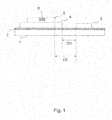
- Fig. 1 a first preferred embodiment of an LED module according to the invention is shown.
- the LED module comprises a base substrate 1 on which an insulation layer 2 is applied over the entire area.
- An LED die 3 embodied as a housing-less semiconductor chip is placed on the insulation layer 2.
- a build-up substrate 4 is formed at a spatial distance D1 from the LED die 3.
- a further semiconductor die 5 having a further electronic component 8 is mounted or formed on the build-up substrate 4 at a spatial distance D2 from the LED die 3.
- the above-described alternative 1 in FIG Fig. 1 shown.
- the further semiconductor die 5 with the one further electronic component 8 can be mounted or formed directly on the insulation layer 2 at a spatial distance D2 from the LED die 3 (this corresponds to the above-described alternative 2, not according to the invention).
- the LED module according to the invention comprises at least one LED die 3 and at least one further semiconductor die 5 having at least one further electronic component 8, the at least one LED die 3 being arranged on the insulation layer 2 and the at least one further Semiconductor die 5 with the at least one further electronic component 8 is arranged at a spatial distance D2 from the at least one LED die 3 on a build-up substrate 4 (alternative 1) formed on the insulation layer 2 or directly on the insulation layer 2 (alternative 2) .
- the embodiment shown is at least one further semiconductor die 5 with at least one further electronic component 8 mounted or formed on a build-up substrate 4 formed on the insulation layer 2 at a spatial distance D2 from the LED die 3 and at least one further semiconductor die 5 with at least Another electronic component 8 is mounted or formed directly on the insulation layer 2 at a spatial distance D2 from the LED die 3.
- the spatial distance D1 corresponds to the minimum distance between the building substrate 4 and the at least one LED die 3.
- the spatial distance between the build-up substrate 4 and each of the LED dice 3 corresponds at least to the spatial distance D1.
- the spatial distance between the building substrate 4 and the individual LED dice 3 can also be greater than the distance D1.
- the spatial distance D2 corresponds to the minimum distance between the at least one further semiconductor die 5 having the at least one further electronic component 8 and the at least one LED die 3.
- the spatial distance between the at least one further semiconductor die 5 and each of the LED dice 3 corresponds to at least the spatial distance D2.
- the spatial distance between the at least one further semiconductor die 5 and individual LED dice 3 can also be greater than the distance D2.
- the distance D2 is greater than the distance D1.
- the distance D2 can also be the same as the distance D1.
- the distance D2 can also be smaller than the distance D1 (see Figure 5a and 5b ).
- the spatial distance D2 corresponds to the at least one further semiconductor die 5 with the at least one further electronic component 8 for the at least one LED die 3, preferably at least 2.5 millimeters (mm).
- the spatial distance D2 from the at least one further semiconductor die 5 corresponds to the at least one further electronic component 8 to the at least one LED die 3, preferably at least 0.4 millimeters (mm).
- the base substrate 1 is preferably made of metal, such as aluminum, silver or copper. Since aluminum, silver or copper cannot be used directly as the base material in order to achieve sufficient insulation from the LED die 3, an insulation layer 2 must be provided.
- the insulation layer 2 is applied to the aluminum substrate 1 as a transparent insulation layer 2, for example.
- This insulation layer 2 can be formed from organic or inorganic material. For example, a silicon layer or a SOL gel siloxane can be used to provide the insulation layer 2.
- the insulation layer 2 ensures that a very high breakdown voltage, for example greater than 4 kilovolts, is required in order to destroy the LED die 3.
- the construction substrate 4 preferably corresponds to a circuit board or circuit board (“ printed circuit board / PCB” ) and is consequently preferably made of a material (PCB material) that is used for circuit boards. Therefore, the building substrate 4 is preferably made of a composite material such as FR-4 or FR-4 material. FR-4 material is used, for example, for classic PCB assembly.
- An LED die 3 or another semiconductor die 5 is preferably arranged on a submount (in Fig. 1 not shown), wherein the submount is preferably made of a ceramic material such as aluminum oxide (Al 2 O 3 ) or aluminum nitride (AlN).
- the LED die 3 or the further semiconductor die 5 can be arranged on the mounting substrate 4 through the submount (in Fig. 1 Not shown).
- a submount preferably has a thickness (layer thickness) between 50 and 200 micrometers ( ⁇ m), particularly preferably between 100 and 150 micrometers ( ⁇ m).
- a field effect transistor embodied as a housing-less semiconductor chip or a microcontroller circuit or a constant current source or a rectifier is preferably embodied as a further electronic component 8 on the build-up substrate 4.
- This further electronic component 8, embodied as a housing-less semiconductor chip, is placed in a further semiconductor die 5 and enables the entire LED module can be manufactured as COB technology.
- the leakage current and the breakdown voltage can be maintained and, moreover, the LED module can be produced in a miniaturized manner.
- a multiplicity of LED dice 3 is preferably formed. Each individual LED dice 3 is encased in a phosphor coating, whereas the other electronic components 8 in the semiconductor die 5 are formed in a periphery outside the first cavity K1 of a build-up substrate 4 (see e.g. Fig. 3 ).
- a metallic top side of the mounting substrate 4 is used in order to connect the further electronic components 8 in an electrically conductive manner and to provide thermal conductivity.
- a ceramic ink is used as the insulating material. This enables a breakdown voltage security of up to 60 volts.
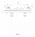
- a second preferred embodiment of an LED module according to the invention is shown.
- the above statements with regard to the preferred embodiment of an LED module according to the invention according to FIG Fig. 1 are essentially for the in Fig. 2 Shown preferred embodiment of an LED module according to the invention applies.
- a plurality of LED dice 3 are mounted on an insulation layer 2 of a base substrate 1.
- the LED dice 3 are arranged in a first cavity K1 of a build-up substrate 4.
- the LED dice 3 are arranged in the further semiconductor dice 5 at a sufficient spatial distance D1 from the construction substrate 4 and at a sufficient spatial distance D2 from the further electronic components 8.
- the spatial distance D1 and the spatial distance D2 are preferably dependent on the diameter of the first cavity K1 and of the LED module, which is preferably a spot light engine module.
- the diameter of the first cavity K1 or of the dam 6 is preferably between 5.8 and 22.8 millimeters (mm), particularly preferably 16.8; 18.8 or 22.8 millimeters (mm).
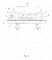
- Fig. 3 a third preferred embodiment of an LED module according to the invention is shown.
- the above statements with regard to the preferred embodiment of an LED module according to the invention according to FIGS Fig. 1 and 2 are essentially for the in Fig. 3 Shown preferred embodiment of an LED module according to the invention applies.
- Additional dams 6 are shown in order to separate the build-up substrate 4 from the LED dice 3 arranged in the first cavity K1.
- each dam 6 are each arranged at a transition or in a border area between the building substrate 4 and the first cavity K1, the dams 6 preferably being formed from the building substrate. That is to say, each dam 6 preferably corresponds to a building substrate whose layer thickness or height is greater than the layer thickness or height of the remaining building substrate 4 in the LED module.
- the build-up substrate 4 preferably has a layer thickness between 0.8 and 3.2 millimeters (mm), preferably between 1.4 and 1.8 millimeters (mm) and very preferably 1.6 millimeters (mm).
- dams 6 are according to Fig. 3 provided to enable the LED dice 3 arranged in the first cavity K1 to be wrapped with a wavelength conversion material 7.
- the dams 6 represent a limitation of the LED dice casing 7.
- This conversion material 7 is, for example, phosphor, in order to form a secondary wavelength from a primary wavelength of the LED die 3, so that a mixed light is produced, which is emitted by the LED module as white light, for example.
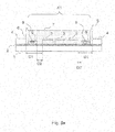
- Fig. 4 a fourth preferred embodiment of an LED module according to the invention is shown.
- the above statements with regard to the preferred embodiment of an LED module according to the invention according to FIGS Fig. 1 , 2 and 3 are essentially for the in Fig. 4 Shown preferred embodiment of an LED module according to the invention applies.
- the at least one further semiconductor die 5 and / or the at least one further electronic component 8 of the at least one further semiconductor die 5 is preferably at least partially encased and / or covered by a reflective potting compound, which preferably corresponds to a reflective dam 6.
- the reflective potting compound preferably represents a reflective polymer matrix, which preferably consists of silicone or epoxy resin (epoxy) with reflective particles.
- the reflective particles correspond, for example, to titanium dioxide (TiO 2 ), aluminum oxide (Al 2 O 3 ), and / or barium titanate (BaTiO 3 ).
- a dam 6 is arranged at both transitions between the building substrate 4 and the first cavity K1, the layer thickness or height of the two dams 6 being greater than the layer thickness or height of the building substrate 4.
- the length of the two dams 6 of the Fig. 4 is greater than the length of the two dams 6 of the Fig. 3 .
- the dams 6 represent a limitation of the LED dice envelope 7.
- This conversion material 7 is, for example, phosphor in order to form a secondary wavelength from a primary wavelength of the LED dice 3, so that a mixed light is produced which is emitted by the LED module, for example is emitted as white light.
- the dams 6 are also provided to the further semiconductor dice 5, which are arranged at a distance D2 from the LED dice 3 in the periphery or the vicinity of the transition between the cavity K1 and the build-up substrate 4 on the build-up substrate 4, and at least partially encasing and / or covering the at least one further electronic component 8.
- the dams 6 are preferably according to FIG Fig. 4 reflective dams, which preferably represent a reflective polymer matrix and preferably consist of silicone or epoxy resin (epoxy) with reflective particles.
- the reflective particles correspond, for example, to titanium dioxide (TiO 2 ), aluminum oxide (Al 2 O 3 ), and / or barium titanate (BaTiO 3 ).
- Figure 5a shows a fifth preferred embodiment of an LED module not according to the invention.
- the above statements with regard to the preferred embodiment of an LED module according to the invention according to FIGS Fig. 1 , 2 , 3 and 4th are essentially for the in Figure 5a Shown preferred embodiment of an LED module according to the invention applies.
- the at least one further semiconductor die 5 having the at least one further electronic component 8 is preferably mounted directly on the insulation layer 2 at a spatial distance D2. Furthermore, the at least one further semiconductor die 5 with the at least one further electronic component 8 is preferably in the periphery or Arranged in the vicinity of the transition between the build-up substrate 4 and the first cavity K1, the at least one further semiconductor die 5 preferably being arranged inside or outside the first cavity K1. Further semiconductor dice 5 can preferably be arranged in the LED module both inside and outside the cavity K1.
- two further semiconductor dice 5, each with a further electronic component 8 are arranged or mounted directly on the insulation layer 2 at a spatial distance D2 from the LED dice 3 in the cavity K1.
- Figure 5a thus shows the case in which the further semiconductor dice 5 are arranged or mounted within the cavity K1 in the periphery or surroundings of the transition between the build-up substrate 4 and the first cavity K1.
- dams 6 are two dams 6 at the two transitions between the cavity K1 and the building substrate 4 according to FIG Figure 5a provided to enable the LED dice 3 arranged in the first cavity K1 to be wrapped with a wavelength conversion material 7.
- the dams 6 represent a limitation of the LED dice envelope 7.
- This conversion material 7 is, for example, phosphor in order to form a secondary wavelength from a primary wavelength of the LED die 3, so that a mixed light is produced which is emitted by the LED module, for example is emitted as white light.
- the length of the dams 6 according to the Figure 5a are shorter than the length of the dams 6 of the Fig. 3 and 4th .
- the two further semiconductor dice 5 arranged in the cavity K1, each having a further electronic component 8, are also encased by the wavelength conversion material 7. Consequently, the at least one LED die 3 and the at least one further semiconductor die 5 having the at least one further electronic component 8 are therefore preferably with a Wavelength conversion material 7 enveloped.
- the distance D2 between the further semiconductor dice 5 and the LED dice 3 is smaller than the spatial distance D1 between the build-up substrate 4 and the LED dice 3.
- the distance D2 can also be greater than (see Fig. 1 , 2 , 3 and 4th ) or equal to the distance D1.
- Figure 5b shows a sixth preferred embodiment of an LED module not according to the invention.
- the above statements with regard to the preferred embodiment of an LED module according to the invention according to FIGS Fig. 1 , 2 , 3 , 4th and 5a are essentially for the in Figure 5b Shown preferred embodiment of an LED module according to the invention applies.
- the LED module according to the Figure 5b corresponds essentially to the LED module according to Figure 5a , whereby in the cavity K1 of the LED module the Figure 5b Between each further semiconductor die 5 and the LED dice 3 a dam 6 is arranged or formed, which separates the respective further semiconductor die 5 from the LED dice 3. According to Figure 5b the formation of two additional dams 6 in the first cavity K1 results in two further cavities K2, in each of which a further semiconductor die 5 having at least one further electronic component 8 is arranged. Consequently, the LED module preferably has at least one second cavity K2, in which the at least one further semiconductor die 5 having the at least one further electronic component 8 is preferably arranged.
- the at least one second cavity K2 is preferably arranged within the first cavity K1.
- the build-up substrate 4 preferably has at least one second cavity K2 (in addition to the first cavity K1).
- a reflective casting compound preferably by a reflective dam 6, at least partially encased and / or covered (not in Figure 5b shown).
- This reflective potting compound or this reflective dam 6 preferably represents a polymer matrix, which preferably consists of silicone or epoxy resin (epoxy) with reflective particles.
- the reflective particles are, for example, titanium dioxide (TiO 2 ), aluminum oxide (Al 2 O 3 ), and / or barium titanate (BaTiO 3 ).
- the two further semiconductor dice 5 in the two second cavities K2 according to FIG Figure 5b and / or the respective at least one further electronic component 8 can be at least partially encased and / or covered by the respective dams 6, the dams 6 then preferably being reflective dams.
- Fig. 6 an exemplary equivalent circuit diagram of a preferred embodiment of an LED module according to the invention is shown.
- an alternating voltage is connected to the mains alternating voltage connections 81.
- the alternating voltage has a level of 230V, for example.
- This alternating voltage is rectified by means of a rectifier 82 and four microcontrollers 83 are provided to which an LED path made up of 84 LEDs 3 is connected.
- This LED path is wired according to the level of the rectified alternating voltage, whereby the microcontroller 83 can bridge parts of the LED path.
- Either or both of the in Fig. 6 Components 83 marked with an asterisk ("*") preferably correspond to a constant current source.
- the LED module thus comprises according to FIG Fig. 6 a further electronic component 8, which corresponds to a rectifier 82, and four further electronic components 8, which Microcontrollers 83 or constant current sources 83 correspond.
- each of the components 82 and 83 is shown in accordance with FIG Fig. 6 arranged as a further electronic component 8 in a semiconductor die 5 on a build-up substrate 4 (alternative 1) or directly on the insulation layer 2 (alternative 2) at a distance D2 from the LED die 3. In this way, complete integration of all circuit components for operating an LED module with AC voltage is obtained.
- a Spot Light Module for Spot Light Engine (SLE) or Spot Light Luminaire applications can thus be provided.
- the leakage current is given a safety margin, thermal conductivity and also rectification of the alternating voltage by means of a single COB module.
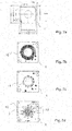
- FIG. 7a to 7d is a seventh preferred embodiment of an LED module according to the invention, partly provided in COB technology and partly in SMT, shown.
- the LED module according to Figures 7a to 7d includes the components of the equivalent circuit according to Fig. 6 .
- Figure 7a the base substrate 1 is shown in plan view. Holes for mounting the LED module are also shown. The dimensions in Figure 7a are to be regarded as exemplary.
- the Figure 7b already shows that the LED module is built in both COB technology and partly in SMT.
- an electrical wiring layer 10 also referred to as a copper top layer, is formed on the insulation layer 2.
- the alternating voltage 81 is applied to this wiring and the SMD components are fitted to it.
- FIG. 11 shows a solder mask layer 11 above the wiring layer 10 according to FIG Figure 7b .
- This solder resist 11 also referred to as a solder mask, soldermask or resist, fulfills different functions on the base substrate 1. It serves to protect the base substrate 1 from corrosion and mechanical damage and, during soldering, prevents wetting of the areas covered with it on the base substrate 1. Furthermore, the solder resist 11 improves the electrical properties such as dielectric strength. Epoxy resin, for example, is used as the material for a solder resist 11.
- the assembly with SMD components on the base substrate 1 is now provided.
- the bridge rectifier 82 with the diodes D1 to D4, the microcontroller or constant current sources 83, the switch Q1 and the diode D5 are off according to the equivalent circuit diagram Fig. 6 attached as SMD parts on the base substrate 1.
- the 84 LED dies 3 are introduced into the interior of the base substrate 1 in the manner indicated above.
- An electrically insulating layer 2, for example a plastic layer, can be applied to the aluminum platform 1 in order to comply with the insulation regulations for direct AC LED modules.
- the LED chips 3 have an insulating sapphire layer on their underside which, however, only has a layer thickness of, for example, 100 micrometers (pm) and thus does not meet the requirements for encapsulated modules with a minimum insulation thickness of 400 micrometers (pm).
- the SMD technology can be combined with the COB technology, whereby costs can be reduced and manufacturing processes can be simplified.
- FIG. 14 is a process flow diagram for a preferred exemplary embodiment of a method 900 according to the invention for producing an LED module in chip-on-board Technology (according to the above-described alternatives 1 and 2 with or without a cavity in a build-up substrate).
- a base substrate 1 is provided.
- an insulation layer 2 is applied over the entire area to the base substrate 1.
- a build-up substrate 4 is arranged on the insulation layer 2.
- the build-up substrate optionally has a first cavity K1.
- the build-up substrate 4 can optionally have at least one second cavity K2, which is preferably formed or arranged in the first cavity K1.
- step 904 at least one LED die 3 is mounted on the insulation layer 2 (if the build-up substrate 4 does not have a first cavity K1) or in the first cavity K1 on the insulation layer 2 (if the build-up substrate 4 has a first cavity K1).
- step 905 at least one further semiconductor die 5, preferably embodied as a housing-free semiconductor chip, is mounted on the build-up substrate 4 (alternative 1 according to the invention) or on the insulation layer 2 (alternative 2 not according to the invention), the semiconductor die 5 having at least one further electronic component 8, with which the LED die 3 is switched.
- the at least one further semiconductor die 5 is preferably arranged or mounted in at least one second cavity K2 in step 905 (if the build-up substrate 4 has at least one second cavity K2).
Landscapes
- Led Device Packages (AREA)
Claims (13)
- Module LED équipé de la technologie chip on board, présentant :a) un substrat de base (1) ; le substrat de base (1) se composant de préférence d'aluminium, d'argent ou de cuivreb) une couche isolante (2) formée sur toute la surface du substrat de base (1) ;c) au moins une puce LED (3) montée directement sur la couche isolante (2) ;d) un substrat de montage (4) formé sur la couche isolante (2) à distance spatiale (D1) de l'au moins une puce LED (3) ; ete) au moins une autre puce à semi-conducteur (5) comportant au moins un autre composant électronique (8) conçu pour le câblage de la puce LED (3) ;f) l'au moins une autre puce à semi-conducteur (5) étant agencée sur le substrat de montage (4) à distance spatiale (D2) de l'au moins une puce LED (3).
- Module LED selon la revendication 1,- le substrat de montage (4) présentant une première cavité (K1) dans laquelle l'au moins une puce LED (3) est agencée, et- l'au moins une autre puce à semi-conducteur (5) étant agencée à la périphérie de la transition entre le substrat de montage (4) et la première cavité (K1).
- Module LED selon la revendication 1 ou 2,- la surface du substrat de base (1) étant optiquement réfléchissante, et- la couche d'isolation (2) étant optiquement transparente ou réfléchissante.
- Module LED selon l'une quelconque des revendications précédentes, dans lequel l'au moins une autre puce à semi-conducteur (5) ou l'au moins une puce LED (3) est montée directement sur le substrat de montage (4), sur la couche isolante (2) ou sur un support sous-jacent, sous la forme d'une puce nue sans boîtier.
- Module LED selon l'une quelconque des revendications précédentes, dans lequel l'au moins un autre composant électronique (8) est un fusible, une résistance, une diode Zener et/ou une diode d'écrêtage, ou dans lequel l'au moins un autre composant électronique (8) est un transistor à effet de champ, un microcontrôleur (83), une source de courant constant (83) ou un redresseur (82).
- Module LED selon l'une quelconque des revendications précédentes,- le module LED présentant au moins une deuxième cavité (K2), et- l'au moins une autre puce à semi-conducteur (5) étant agencée dans l'au moins une deuxième cavité (K2).
- Module LED selon l'une quelconque des revendications précédentes,- l'au moins une puce LED (3) étant enveloppée d'un matériau de conversion de longueur d'onde (7), ou- l'au moins une puce LED (3) et l'au moins une autre puce à semi-conducteur (5) étant enveloppées d'un matériau de conversion de longueur d'onde (7).
- Module LED selon l'une quelconque des revendications précédentes, dans lequel l'au moins une autre puce à semi-conducteur (5) est enveloppée et/ou recouverte d'un composé d'enrobage réfléchissant ou transparent.
- Module LED selon l'une quelconque des revendications précédentes, ledit module LED présentant un fusible en guise d'au moins un autre composant électronique (8), le fusible étant conçu sous la forme d'un fil de connexion dans une cavité (K) du substrat de montage (4), ou
le module à LED comportant un fusible en guise d'au moins un autre composant électronique (8), le fusible étant conçu sous la forme d'une boucle de fil. - Module LED selon l'une quelconque des revendications précédentes, dans lequel le substrat de montage (4) présente une surface métallique sur laquelle est agencé l'au moins un autre composant électronique (8).
- Procédé (900) pour la fabrication d'un module LED équipé de la technologie chip on board selon l'une des revendications précédentes, le procédé comprenant les étapes suivantes :a) mise à disposition (901) d'un substrat de base (1) ;b) application (902) d'une couche isolante (2) sur toute la surface du substrat de base (1) ;c) montage (905) d'au moins une puce LED (3) sur la couche isolante (2) ;d) formation (903) d'un substrat de montage (4) sur la couche isolante (2) à distance spatiale (D1) de l'au moins une puce LED (3) ;e) montage (906) d'au moins une autre puce à semi-conducteur (5) dans le module LED, l'au moins une autre puce à semi-conducteur (5) présentant au moins un autre composant électronique (8) conçu pour le câblage de la puce LED (3) ; etf) montage (906) de l'au moins une autre puce à semi-conducteur (5) sur le substrat de montage (4) à distance spatiale (D2) de l'au moins une puce LED (3).
- Procédé (900) selon la revendication 11, dans lequel le substrat de montage (4) présente une première cavité (K1), le procédé comprenant en outre les étapes suivantes :- montage (905) de l'au moins une puce LED (3) dans la première cavité (K1) sur la couche isolante (2), et- agencement de l'au moins une autre puce à semi-conducteur (5) à la périphérie de la transition entre le substrat de montage (4) et la première cavité (K1).
- Procédé (900) selon la revendication 11 ou 12, présentant en outre l'étape suivante :- enveloppement de l'au moins une puce LED (3) avec un matériau de conversion de longueur d'onde (7), ou- enveloppement de l'au moins une puce LED (3) et de l'au moins une autre puce à semi-conducteur (5) avec un matériau de conversion de longueur d'onde (7).
Applications Claiming Priority (1)
| Application Number | Priority Date | Filing Date | Title |
|---|---|---|---|
| DE102016205691.3A DE102016205691A1 (de) | 2016-04-06 | 2016-04-06 | LED-Modul in Chip-on-Board-Technologie |
Publications (2)
| Publication Number | Publication Date |
|---|---|
| EP3229269A1 EP3229269A1 (fr) | 2017-10-11 |
| EP3229269B1 true EP3229269B1 (fr) | 2021-07-21 |
Family
ID=58489198
Family Applications (1)
| Application Number | Title | Priority Date | Filing Date |
|---|---|---|---|
| EP17164575.7A Active EP3229269B1 (fr) | 2016-04-06 | 2017-04-03 | Module del selon une technologie chip on board |
Country Status (2)
| Country | Link |
|---|---|
| EP (1) | EP3229269B1 (fr) |
| DE (1) | DE102016205691A1 (fr) |
Families Citing this family (3)
| Publication number | Priority date | Publication date | Assignee | Title |
|---|---|---|---|---|
| DE102017106959A1 (de) | 2017-03-31 | 2018-10-04 | Osram Opto Semiconductors Gmbh | Leuchtvorrichtung und Leuchtsystem |
| CN113497075B (zh) * | 2020-04-01 | 2024-06-11 | 刘台徽 | 全彩微型发光二极管封装体及其封装方法 |
| CN112967935B (zh) * | 2021-02-09 | 2022-04-15 | 池州昀冢电子科技有限公司 | 封装结构及其制备方法 |
Family Cites Families (8)
| Publication number | Priority date | Publication date | Assignee | Title |
|---|---|---|---|---|
| DE29621154U1 (de) * | 1996-12-05 | 1998-04-02 | Wickmann-Werke GmbH, 58453 Witten | Elektrische Sicherung |
| DE102009010179A1 (de) * | 2009-02-23 | 2010-09-02 | Osram Gesellschaft mit beschränkter Haftung | Leuchtmodul mit Reflektorwand |
| US8608340B2 (en) * | 2010-06-28 | 2013-12-17 | Toshiba Lighting & Technology Corporation | Light-emitting module and lighting apparatus with the same |
| DE102012101560B4 (de) * | 2011-10-27 | 2016-02-04 | Epcos Ag | Leuchtdiodenvorrichtung |
| CN203910842U (zh) | 2011-12-20 | 2014-10-29 | 西铁城控股株式会社 | Led模块 |
| KR20130090644A (ko) * | 2012-02-06 | 2013-08-14 | 주식회사 두성에이텍 | 개별 반사 구조를 갖는 pcb 및 이를 이용한 발광 다이오드 패키지 제조 방법 |
| DE102012104494A1 (de) * | 2012-05-24 | 2013-11-28 | Epcos Ag | Leuchtdiodenvorrichtung |
| DE102014205470B4 (de) * | 2014-03-24 | 2016-10-13 | Osram Gmbh | Leuchtvorrichtung mit CoB-Bereich |
-
2016
- 2016-04-06 DE DE102016205691.3A patent/DE102016205691A1/de not_active Withdrawn
-
2017
- 2017-04-03 EP EP17164575.7A patent/EP3229269B1/fr active Active
Non-Patent Citations (1)
| Title |
|---|
| None * |
Also Published As
| Publication number | Publication date |
|---|---|
| DE102016205691A1 (de) | 2017-10-12 |
| EP3229269A1 (fr) | 2017-10-11 |
Similar Documents
| Publication | Publication Date | Title |
|---|---|---|
| DE102004044149B4 (de) | Hochleistungs-Leuchtdiodenvorrichtung | |
| EP2815177B1 (fr) | Module d'éclairage | |
| WO2014122061A1 (fr) | Module d'éclairage optoélectronique, dispositif d'éclairage optoélectronique et projecteur de véhicule automobile | |
| EP2815439A1 (fr) | Module de led comprenant un support à haute réflectivité | |
| DE112016002072B4 (de) | Emissionseinrichtung für ultraviolette strahlen | |
| DE102010016720B4 (de) | Leuchtdiodenanordnung für hohe Sicherheitsanforderungen | |
| WO2017190895A1 (fr) | Système à diodes électroluminescentes multiples | |
| EP2888745B1 (fr) | Ensemble composant électrique | |
| DE102017104606A1 (de) | Lichtemittierender Apparat und Beleuchtungsapparat | |
| WO2016202609A1 (fr) | Agencement de diodes luminescentes et procédé de fabrication d'un agencement de diodes luminescentes | |
| EP3229269B1 (fr) | Module del selon une technologie chip on board | |
| EP2609633B1 (fr) | Composant émetteur de rayonnement et procédé de fabrication d'un composant émetteur de rayonnement | |
| DE102012202353A1 (de) | Leuchtmodul-Leiterplatte | |
| DE102017102619B4 (de) | LED-Einheit und LED-Modul | |
| DE102016116617A1 (de) | Lichtemittierende Vorrichtung | |
| DE102018100115A1 (de) | Montierungssubstrat, Licht emittierende Einrichtung und Beleuchtungseinrichtung | |
| WO2013060868A1 (fr) | Dispositif à diode électroluminescente comprenant des composants encastrés | |
| DE102017101769A1 (de) | Verfahren zum herstellen einer optoelektronischen faser und optoelektronische faser | |
| DE102013207111B4 (de) | Optoelektronisches Bauelement | |
| DE102016114175A1 (de) | Licht emittierende Einrichtung und Beleuchtungseinrichtung | |
| WO2017001327A1 (fr) | Dispositif d'éclairage optoélectronique | |
| WO2017129697A1 (fr) | Composant optoélectronique à contacts latéraux | |
| EP2626918B1 (fr) | Module à DEL avec un substrat de haute reflectivité et procédé de fabrication d'un module à DEL avec un substrat de haute reflectivité | |
| DE102015117936A1 (de) | Optoelektronische Leuchtvorrichtung | |
| DE102016114277B4 (de) | Lichtemittierendes Bauteil |
Legal Events
| Date | Code | Title | Description |
|---|---|---|---|
| PUAI | Public reference made under article 153(3) epc to a published international application that has entered the european phase |
Free format text: ORIGINAL CODE: 0009012 |
|
| STAA | Information on the status of an ep patent application or granted ep patent |
Free format text: STATUS: THE APPLICATION HAS BEEN PUBLISHED |
|
| AK | Designated contracting states |
Kind code of ref document: A1 Designated state(s): AL AT BE BG CH CY CZ DE DK EE ES FI FR GB GR HR HU IE IS IT LI LT LU LV MC MK MT NL NO PL PT RO RS SE SI SK SM TR |
|
| AX | Request for extension of the european patent |
Extension state: BA ME |
|
| STAA | Information on the status of an ep patent application or granted ep patent |
Free format text: STATUS: REQUEST FOR EXAMINATION WAS MADE |
|
| 17P | Request for examination filed |
Effective date: 20180116 |
|
| RBV | Designated contracting states (corrected) |
Designated state(s): AL AT BE BG CH CY CZ DE DK EE ES FI FR GB GR HR HU IE IS IT LI LT LU LV MC MK MT NL NO PL PT RO RS SE SI SK SM TR |
|
| STAA | Information on the status of an ep patent application or granted ep patent |
Free format text: STATUS: EXAMINATION IS IN PROGRESS |
|
| 17Q | First examination report despatched |
Effective date: 20190521 |
|
| RAP1 | Party data changed (applicant data changed or rights of an application transferred) |
Owner name: TRIDONIC GMBH & CO. KG |
|
| GRAP | Despatch of communication of intention to grant a patent |
Free format text: ORIGINAL CODE: EPIDOSNIGR1 |
|
| STAA | Information on the status of an ep patent application or granted ep patent |
Free format text: STATUS: GRANT OF PATENT IS INTENDED |
|
| INTG | Intention to grant announced |
Effective date: 20210426 |
|
| GRAS | Grant fee paid |
Free format text: ORIGINAL CODE: EPIDOSNIGR3 |
|
| GRAA | (expected) grant |
Free format text: ORIGINAL CODE: 0009210 |
|
| STAA | Information on the status of an ep patent application or granted ep patent |
Free format text: STATUS: THE PATENT HAS BEEN GRANTED |
|
| AK | Designated contracting states |
Kind code of ref document: B1 Designated state(s): AL AT BE BG CH CY CZ DE DK EE ES FI FR GB GR HR HU IE IS IT LI LT LU LV MC MK MT NL NO PL PT RO RS SE SI SK SM TR |
|
| REG | Reference to a national code |
Ref country code: GB Ref legal event code: FG4D Free format text: NOT ENGLISH |
|
| REG | Reference to a national code |
Ref country code: CH Ref legal event code: EP |
|
| REG | Reference to a national code |
Ref country code: DE Ref legal event code: R096 Ref document number: 502017010936 Country of ref document: DE |
|
| REG | Reference to a national code |
Ref country code: AT Ref legal event code: REF Ref document number: 1413391 Country of ref document: AT Kind code of ref document: T Effective date: 20210815 |
|
| REG | Reference to a national code |
Ref country code: IE Ref legal event code: FG4D Free format text: LANGUAGE OF EP DOCUMENT: GERMAN |
|
| REG | Reference to a national code |
Ref country code: LT Ref legal event code: MG9D |
|
| REG | Reference to a national code |
Ref country code: NL Ref legal event code: MP Effective date: 20210721 |
|
| PG25 | Lapsed in a contracting state [announced via postgrant information from national office to epo] |
Ref country code: RS Free format text: LAPSE BECAUSE OF FAILURE TO SUBMIT A TRANSLATION OF THE DESCRIPTION OR TO PAY THE FEE WITHIN THE PRESCRIBED TIME-LIMIT Effective date: 20210721 Ref country code: SE Free format text: LAPSE BECAUSE OF FAILURE TO SUBMIT A TRANSLATION OF THE DESCRIPTION OR TO PAY THE FEE WITHIN THE PRESCRIBED TIME-LIMIT Effective date: 20210721 Ref country code: BG Free format text: LAPSE BECAUSE OF FAILURE TO SUBMIT A TRANSLATION OF THE DESCRIPTION OR TO PAY THE FEE WITHIN THE PRESCRIBED TIME-LIMIT Effective date: 20211021 Ref country code: LT Free format text: LAPSE BECAUSE OF FAILURE TO SUBMIT A TRANSLATION OF THE DESCRIPTION OR TO PAY THE FEE WITHIN THE PRESCRIBED TIME-LIMIT Effective date: 20210721 Ref country code: PT Free format text: LAPSE BECAUSE OF FAILURE TO SUBMIT A TRANSLATION OF THE DESCRIPTION OR TO PAY THE FEE WITHIN THE PRESCRIBED TIME-LIMIT Effective date: 20211122 Ref country code: NL Free format text: LAPSE BECAUSE OF FAILURE TO SUBMIT A TRANSLATION OF THE DESCRIPTION OR TO PAY THE FEE WITHIN THE PRESCRIBED TIME-LIMIT Effective date: 20210721 Ref country code: NO Free format text: LAPSE BECAUSE OF FAILURE TO SUBMIT A TRANSLATION OF THE DESCRIPTION OR TO PAY THE FEE WITHIN THE PRESCRIBED TIME-LIMIT Effective date: 20211021 Ref country code: ES Free format text: LAPSE BECAUSE OF FAILURE TO SUBMIT A TRANSLATION OF THE DESCRIPTION OR TO PAY THE FEE WITHIN THE PRESCRIBED TIME-LIMIT Effective date: 20210721 Ref country code: FI Free format text: LAPSE BECAUSE OF FAILURE TO SUBMIT A TRANSLATION OF THE DESCRIPTION OR TO PAY THE FEE WITHIN THE PRESCRIBED TIME-LIMIT Effective date: 20210721 Ref country code: HR Free format text: LAPSE BECAUSE OF FAILURE TO SUBMIT A TRANSLATION OF THE DESCRIPTION OR TO PAY THE FEE WITHIN THE PRESCRIBED TIME-LIMIT Effective date: 20210721 |
|
| PG25 | Lapsed in a contracting state [announced via postgrant information from national office to epo] |
Ref country code: PL Free format text: LAPSE BECAUSE OF FAILURE TO SUBMIT A TRANSLATION OF THE DESCRIPTION OR TO PAY THE FEE WITHIN THE PRESCRIBED TIME-LIMIT Effective date: 20210721 Ref country code: LV Free format text: LAPSE BECAUSE OF FAILURE TO SUBMIT A TRANSLATION OF THE DESCRIPTION OR TO PAY THE FEE WITHIN THE PRESCRIBED TIME-LIMIT Effective date: 20210721 Ref country code: GR Free format text: LAPSE BECAUSE OF FAILURE TO SUBMIT A TRANSLATION OF THE DESCRIPTION OR TO PAY THE FEE WITHIN THE PRESCRIBED TIME-LIMIT Effective date: 20211022 |
|
| REG | Reference to a national code |
Ref country code: DE Ref legal event code: R097 Ref document number: 502017010936 Country of ref document: DE |
|
| PG25 | Lapsed in a contracting state [announced via postgrant information from national office to epo] |
Ref country code: DK Free format text: LAPSE BECAUSE OF FAILURE TO SUBMIT A TRANSLATION OF THE DESCRIPTION OR TO PAY THE FEE WITHIN THE PRESCRIBED TIME-LIMIT Effective date: 20210721 |
|
| PLBE | No opposition filed within time limit |
Free format text: ORIGINAL CODE: 0009261 |
|
| STAA | Information on the status of an ep patent application or granted ep patent |
Free format text: STATUS: NO OPPOSITION FILED WITHIN TIME LIMIT |
|
| PG25 | Lapsed in a contracting state [announced via postgrant information from national office to epo] |
Ref country code: SM Free format text: LAPSE BECAUSE OF FAILURE TO SUBMIT A TRANSLATION OF THE DESCRIPTION OR TO PAY THE FEE WITHIN THE PRESCRIBED TIME-LIMIT Effective date: 20210721 Ref country code: SK Free format text: LAPSE BECAUSE OF FAILURE TO SUBMIT A TRANSLATION OF THE DESCRIPTION OR TO PAY THE FEE WITHIN THE PRESCRIBED TIME-LIMIT Effective date: 20210721 Ref country code: RO Free format text: LAPSE BECAUSE OF FAILURE TO SUBMIT A TRANSLATION OF THE DESCRIPTION OR TO PAY THE FEE WITHIN THE PRESCRIBED TIME-LIMIT Effective date: 20210721 Ref country code: EE Free format text: LAPSE BECAUSE OF FAILURE TO SUBMIT A TRANSLATION OF THE DESCRIPTION OR TO PAY THE FEE WITHIN THE PRESCRIBED TIME-LIMIT Effective date: 20210721 Ref country code: CZ Free format text: LAPSE BECAUSE OF FAILURE TO SUBMIT A TRANSLATION OF THE DESCRIPTION OR TO PAY THE FEE WITHIN THE PRESCRIBED TIME-LIMIT Effective date: 20210721 Ref country code: AL Free format text: LAPSE BECAUSE OF FAILURE TO SUBMIT A TRANSLATION OF THE DESCRIPTION OR TO PAY THE FEE WITHIN THE PRESCRIBED TIME-LIMIT Effective date: 20210721 |
|
| 26N | No opposition filed |
Effective date: 20220422 |
|
| PG25 | Lapsed in a contracting state [announced via postgrant information from national office to epo] |
Ref country code: IT Free format text: LAPSE BECAUSE OF FAILURE TO SUBMIT A TRANSLATION OF THE DESCRIPTION OR TO PAY THE FEE WITHIN THE PRESCRIBED TIME-LIMIT Effective date: 20210721 |
|
| PGFP | Annual fee paid to national office [announced via postgrant information from national office to epo] |
Ref country code: GB Payment date: 20220419 Year of fee payment: 6 Ref country code: FR Payment date: 20220427 Year of fee payment: 6 |
|
| PGFP | Annual fee paid to national office [announced via postgrant information from national office to epo] |
Ref country code: AT Payment date: 20220419 Year of fee payment: 6 |
|
| REG | Reference to a national code |
Ref country code: CH Ref legal event code: PL |
|
| REG | Reference to a national code |
Ref country code: BE Ref legal event code: MM Effective date: 20220430 |
|
| REG | Reference to a national code |
Ref country code: DE Ref legal event code: R084 Ref document number: 502017010936 Country of ref document: DE |
|
| PG25 | Lapsed in a contracting state [announced via postgrant information from national office to epo] |
Ref country code: MC Free format text: LAPSE BECAUSE OF FAILURE TO SUBMIT A TRANSLATION OF THE DESCRIPTION OR TO PAY THE FEE WITHIN THE PRESCRIBED TIME-LIMIT Effective date: 20210721 Ref country code: LU Free format text: LAPSE BECAUSE OF NON-PAYMENT OF DUE FEES Effective date: 20220403 Ref country code: LI Free format text: LAPSE BECAUSE OF NON-PAYMENT OF DUE FEES Effective date: 20220430 Ref country code: CH Free format text: LAPSE BECAUSE OF NON-PAYMENT OF DUE FEES Effective date: 20220430 |
|
| PG25 | Lapsed in a contracting state [announced via postgrant information from national office to epo] |
Ref country code: BE Free format text: LAPSE BECAUSE OF NON-PAYMENT OF DUE FEES Effective date: 20220430 |
|
| PG25 | Lapsed in a contracting state [announced via postgrant information from national office to epo] |
Ref country code: IE Free format text: LAPSE BECAUSE OF NON-PAYMENT OF DUE FEES Effective date: 20220403 |
|
| P01 | Opt-out of the competence of the unified patent court (upc) registered |
Effective date: 20230530 |
|
| PGFP | Annual fee paid to national office [announced via postgrant information from national office to epo] |
Ref country code: DE Payment date: 20230427 Year of fee payment: 7 |
|
| REG | Reference to a national code |
Ref country code: AT Ref legal event code: MM01 Ref document number: 1413391 Country of ref document: AT Kind code of ref document: T Effective date: 20230403 |
|
| GBPC | Gb: european patent ceased through non-payment of renewal fee |
Effective date: 20230403 |
|
| PG25 | Lapsed in a contracting state [announced via postgrant information from national office to epo] |
Ref country code: GB Free format text: LAPSE BECAUSE OF NON-PAYMENT OF DUE FEES Effective date: 20230403 |
|
| PG25 | Lapsed in a contracting state [announced via postgrant information from national office to epo] |
Ref country code: GB Free format text: LAPSE BECAUSE OF NON-PAYMENT OF DUE FEES Effective date: 20230403 Ref country code: FR Free format text: LAPSE BECAUSE OF NON-PAYMENT OF DUE FEES Effective date: 20230430 Ref country code: AT Free format text: LAPSE BECAUSE OF NON-PAYMENT OF DUE FEES Effective date: 20230403 |
|
| PG25 | Lapsed in a contracting state [announced via postgrant information from national office to epo] |
Ref country code: HU Free format text: LAPSE BECAUSE OF FAILURE TO SUBMIT A TRANSLATION OF THE DESCRIPTION OR TO PAY THE FEE WITHIN THE PRESCRIBED TIME-LIMIT; INVALID AB INITIO Effective date: 20170403 |
|
| PG25 | Lapsed in a contracting state [announced via postgrant information from national office to epo] |
Ref country code: MK Free format text: LAPSE BECAUSE OF FAILURE TO SUBMIT A TRANSLATION OF THE DESCRIPTION OR TO PAY THE FEE WITHIN THE PRESCRIBED TIME-LIMIT Effective date: 20210721 Ref country code: CY Free format text: LAPSE BECAUSE OF FAILURE TO SUBMIT A TRANSLATION OF THE DESCRIPTION OR TO PAY THE FEE WITHIN THE PRESCRIBED TIME-LIMIT Effective date: 20210721 |
|
| PG25 | Lapsed in a contracting state [announced via postgrant information from national office to epo] |
Ref country code: MT Free format text: LAPSE BECAUSE OF FAILURE TO SUBMIT A TRANSLATION OF THE DESCRIPTION OR TO PAY THE FEE WITHIN THE PRESCRIBED TIME-LIMIT Effective date: 20210721 |
|
| REG | Reference to a national code |
Ref country code: DE Ref legal event code: R119 Ref document number: 502017010936 Country of ref document: DE |
|
| PG25 | Lapsed in a contracting state [announced via postgrant information from national office to epo] |
Ref country code: DE Free format text: LAPSE BECAUSE OF NON-PAYMENT OF DUE FEES Effective date: 20241105 |
|
| PG25 | Lapsed in a contracting state [announced via postgrant information from national office to epo] |
Ref country code: DE Free format text: LAPSE BECAUSE OF NON-PAYMENT OF DUE FEES Effective date: 20241105 |
|
| PG25 | Lapsed in a contracting state [announced via postgrant information from national office to epo] |
Ref country code: TR Free format text: LAPSE BECAUSE OF FAILURE TO SUBMIT A TRANSLATION OF THE DESCRIPTION OR TO PAY THE FEE WITHIN THE PRESCRIBED TIME-LIMIT Effective date: 20210721 |