EP3229285A1 - Pixeldefinitionsschicht und herstellungsverfahren dafür, anzeigetafel und anzeigevorrichtung - Google Patents
Pixeldefinitionsschicht und herstellungsverfahren dafür, anzeigetafel und anzeigevorrichtung Download PDFInfo
- Publication number
- EP3229285A1 EP3229285A1 EP15831209.0A EP15831209A EP3229285A1 EP 3229285 A1 EP3229285 A1 EP 3229285A1 EP 15831209 A EP15831209 A EP 15831209A EP 3229285 A1 EP3229285 A1 EP 3229285A1
- Authority
- EP
- European Patent Office
- Prior art keywords
- pixel defining
- defining layer
- layer
- openings
- correspondence
- Prior art date
- Legal status (The legal status is an assumption and is not a legal conclusion. Google has not performed a legal analysis and makes no representation as to the accuracy of the status listed.)
- Granted
Links
Images


Classifications
-
- H—ELECTRICITY
- H10—SEMICONDUCTOR DEVICES; ELECTRIC SOLID-STATE DEVICES NOT OTHERWISE PROVIDED FOR
- H10K—ORGANIC ELECTRIC SOLID-STATE DEVICES
- H10K50/00—Organic light-emitting devices
- H10K50/10—OLEDs or polymer light-emitting diodes [PLED]
- H10K50/11—OLEDs or polymer light-emitting diodes [PLED] characterised by the electroluminescent [EL] layers
-
- H—ELECTRICITY
- H10—SEMICONDUCTOR DEVICES; ELECTRIC SOLID-STATE DEVICES NOT OTHERWISE PROVIDED FOR
- H10K—ORGANIC ELECTRIC SOLID-STATE DEVICES
- H10K59/00—Integrated devices, or assemblies of multiple devices, comprising at least one organic light-emitting element covered by group H10K50/00
- H10K59/10—OLED displays
- H10K59/12—Active-matrix OLED [AMOLED] displays
- H10K59/122—Pixel-defining structures or layers, e.g. banks
-
- H—ELECTRICITY
- H10—SEMICONDUCTOR DEVICES; ELECTRIC SOLID-STATE DEVICES NOT OTHERWISE PROVIDED FOR
- H10K—ORGANIC ELECTRIC SOLID-STATE DEVICES
- H10K50/00—Organic light-emitting devices
- H10K50/80—Constructional details
-
- H—ELECTRICITY
- H10—SEMICONDUCTOR DEVICES; ELECTRIC SOLID-STATE DEVICES NOT OTHERWISE PROVIDED FOR
- H10K—ORGANIC ELECTRIC SOLID-STATE DEVICES
- H10K59/00—Integrated devices, or assemblies of multiple devices, comprising at least one organic light-emitting element covered by group H10K50/00
-
- H—ELECTRICITY
- H10—SEMICONDUCTOR DEVICES; ELECTRIC SOLID-STATE DEVICES NOT OTHERWISE PROVIDED FOR
- H10K—ORGANIC ELECTRIC SOLID-STATE DEVICES
- H10K59/00—Integrated devices, or assemblies of multiple devices, comprising at least one organic light-emitting element covered by group H10K50/00
- H10K59/10—OLED displays
- H10K59/12—Active-matrix OLED [AMOLED] displays
- H10K59/121—Active-matrix OLED [AMOLED] displays characterised by the geometry or disposition of pixel elements
-
- H—ELECTRICITY
- H10—SEMICONDUCTOR DEVICES; ELECTRIC SOLID-STATE DEVICES NOT OTHERWISE PROVIDED FOR
- H10K—ORGANIC ELECTRIC SOLID-STATE DEVICES
- H10K59/00—Integrated devices, or assemblies of multiple devices, comprising at least one organic light-emitting element covered by group H10K50/00
- H10K59/80—Constructional details
- H10K59/88—Dummy elements, i.e. elements having non-functional features
-
- H—ELECTRICITY
- H10—SEMICONDUCTOR DEVICES; ELECTRIC SOLID-STATE DEVICES NOT OTHERWISE PROVIDED FOR
- H10K—ORGANIC ELECTRIC SOLID-STATE DEVICES
- H10K71/00—Manufacture or treatment specially adapted for the organic devices covered by this subclass
-
- H—ELECTRICITY
- H10—SEMICONDUCTOR DEVICES; ELECTRIC SOLID-STATE DEVICES NOT OTHERWISE PROVIDED FOR
- H10K—ORGANIC ELECTRIC SOLID-STATE DEVICES
- H10K71/00—Manufacture or treatment specially adapted for the organic devices covered by this subclass
- H10K71/10—Deposition of organic active material
- H10K71/191—Deposition of organic active material characterised by provisions for the orientation or alignment of the layer to be deposited
-
- H—ELECTRICITY
- H10—SEMICONDUCTOR DEVICES; ELECTRIC SOLID-STATE DEVICES NOT OTHERWISE PROVIDED FOR
- H10K—ORGANIC ELECTRIC SOLID-STATE DEVICES
- H10K2102/00—Constructional details relating to the organic devices covered by this subclass
- H10K2102/301—Details of OLEDs
- H10K2102/302—Details of OLEDs of OLED structures
-
- H—ELECTRICITY
- H10—SEMICONDUCTOR DEVICES; ELECTRIC SOLID-STATE DEVICES NOT OTHERWISE PROVIDED FOR
- H10K—ORGANIC ELECTRIC SOLID-STATE DEVICES
- H10K71/00—Manufacture or treatment specially adapted for the organic devices covered by this subclass
- H10K71/10—Deposition of organic active material
- H10K71/12—Deposition of organic active material using liquid deposition, e.g. spin coating
Definitions
- the present invention relates to the field of display technology, and particularly to a pixel defining layer and a manufacturing method thereof, a display panel and a display device.
- Method for manufacturing OLED/PLED displays by using solution processes has many advantages and potentials such as low cost, high yield and capability to easily reach large size, and is a potential development direction of the OLED technology.
- OLED/PLED technology it is required to use an organic or inorganic material to manufacture a pixel defining layer, to define an organic material for emitting light within sub-pixel regions defined in the pixel defining layer, so as to achieve high resolution and full color display.
- an anode 102 when an organic light emitting device is manufactured by using inkjet printing or nozzle printing, an anode 102 is usually formed of an hydrophilic transparent conductive film (such as ITO film), and for a good attachment with the anode 102, the solvent for forming an organic light emitting material layer 104 (including a hole transport layer and a hole injection layer) is also hydrophilic.
- the pixel defining layer 103 is usually formed of positive photoresist.
- the pixel defining layer 103 is formed of positive photoresist, after being exposed and developed, the pixel defining layer 103 may have an inverted trapezoidal shape (which is wide at top and narrow at bottom), which has a proper slope angle and thus may reduce breakage of the organic material film layer or the cathode film layer.
- the positive photoresist has hydrophobicity, resulting in poor attachment between the hydrophilic organic material solvent and the hydrophobic pixel defining layer, the formed organic light emitting material layer 104 may contract and thus the cathode 105 and the anode 102 may have a short circuit therebetween, causing adverse display of the display device, and it should be noted that, in the figure, 101 represents the substrate.
- both the pixel defining layer and the organic material solvent are hydrophilic, avoiding the contraction of the organic material, and thus restraining short between the cathode and the anode.
- the pixel defining layer formed of negative photoresist has a regular trapezoidal shape (which is narrow at top and wide at bottom), as shown in Figure 1(b) , the slope angle of the regular trapezoid is improper, so that the cathode is intended to be open, thus resulting in adverse display of the display device.
- the present invention proposes a pixel defining layer and a manufacturing method thereof, a display panel and a display device, which can prevent the short-circuiting between the cathode and the anode and the phenomenon that the cathode is in an open state from easily occurring in the organic light emitting device manufactured by using an inkjet printing method or a nozzle print method.
- the present invention provides a pixel defining layer comprising a first pixel defining layer and a second pixel defining layer stacked on the first pixel defining layer, wherein the first pixel defining layer has a plurality of first openings corresponding to light-emitting regions of respective sub-pixels in one-to-one correspondence, the second pixel defining layer has a plurality of second openings corresponding to the plurality of first openings in one-to-one correspondence, cross section of the first opening being in a regular trapezoidal shape which is narrow at top and wide at bottom, and a cross section of the second opening is in an inverted trapezoidal shape which is wide at top and narrow at bottom.
- the first pixel defining layer is a hydrophilic film layer
- the second pixel defining layer is a hydrophobic film layer
- the hydrophilic film layer is a negative photoresist film layer
- the hydrophobic film layer is a positive photoresist film layer
- a thickness of the first pixel defining layer is smaller than that of the second pixel defining layer.
- the thickness of the first pixel defining layer is between 2000 ⁇ 5000 ⁇ , and the thickness of the second pixel defining layer is between 5000 ⁇ 15000 ⁇ .
- the present invention provides a display panel comprising the above pixel defining layer formed on a substrate.
- the plurality of first openings of the first pixel defining layer are formed therein with anode layers and organic light-emitting layers of respective sub-pixels, the organic light-emitting layer is on the anode layer, and a sum of thicknesses of the organic light-emitting layer and the anode layer is identical to or larger than the thickness of the first pixel defining layer.
- the plurality of second openings of the second pixel defining layer are formed therein with cathode layers of respective sub-pixels, and the cathode layer is on the organic light-emitting layer.
- the present invention provides a display device comprising the above display panel.
- the present invention provides a manufacturing method of a pixel defining layer comprising:
- the step of forming a hydrophilic film layer on a substrate, and patterning the hydrophilic film layer to form a first pixel defining layer having a plurality of first openings corresponding to light-emitting regions of respective sub-pixels in one-to-one correspondence comprises:
- the step of forming a hydrophobic film layer on the substrate formed with the first pixel defining layer thereon, and patterning the hydrophobic film layer to form a second pixel defining layer having a plurality of second openings corresponding to the plurality of first openings in one-to-one correspondence comprises:
- two pixel defining layers i.e., the first pixel defining layer and the second pixel defining layer, are adopted to constitute one pixel defining layer for defining light emitting regions of respective sub-pixel units, and the first pixel defining layer is a hydrophilic film layer, and the second pixel defining layer is a hydrophobic film layer.
- the organic light emitting material may be well attached to the first pixel defining layer due to the hydrophilicity thereof, and may completely cover the anode layer in the light emitting region, thus even after the cathode is formed sequentially, short-circuiting between the anode and the cathode due to contraction of the organic light emitting layer may be avoided.
- the hydrophobic second pixel defining layer is formed on the first pixel defining layer, the second pixel defining layer has a plurality of second openings corresponding to the plurality of first openings in one-to-one correspondence, and cross section of the second opening is in an inverted trapezoidal shape which is wide at top and narrow at bottom. Therefore, the phenomenon that the cathode is in an open state when forming the cathode above the organic light emitting layer may be avoided.
- Fig.2(a) and Fig.2(b) show structural diagrams of a pixel defining layer according to an embodiment in the present invention.
- the pixel defining layer comprises a first pixel defining layer 202 and a second pixel defining layer 203 stacked on the first pixel defining layer 202, wherein the first pixel layer 202 has a plurality of first openings 204 corresponding to light-emitting regions of respective sub-pixels in one-to-one correspondence, the second pixel defining layer 204 has a plurality of second openings 205 corresponding to the plurality of first openings 204 in one-to-one correspondence, cross section of the first opening 204 is in a regular trapezoidal shape which is narrow at top and wide at bottom, and cross section of the second opening 205 is in an inverted trapezoidal shape which is wide at top and narrow at bottom, and as an example, only one first opening 204 and one second opening 205 are illustrated in Fig.2(a) and Fig.2(b) .
- the first pixel defining layer 202 is a hydrophilic film layer
- the second pixel defining layer 203 is a hydrophobic film layer.
- the hydrophilic film layer is formed of negative photoresist
- the hydrophobic film layer is formed of positive photoresist
- the plurality of openings formed in the pixel defining layer are used to define the light emitting regions of the respective sub-pixel units, organic light emitting material solution may be formed in the light emitting regions through printing, and therefore, the pixel defining layer can well prevent the color mixture of organic light emitting materials in respective sub-pixel units of different colors.
- the pixel defining layer may be formed of photoresist, in the present invention, in view of the phenomenon of short between the cathode and the anode or the phenomenon of open of the cathode due to contraction of the organic light emitting material when the pixel defining layer is manufactured by using the photoresist, two pixel defining layers, i.e., the first pixel defining layer 202 and the second pixel defining layer 203, are adopted to constitute one pixel defining layer for defining light emitting regions of the respective sub-pixel units, and the first pixel defining layer 202 is a hydrophilic film layer, and the second pixel defining layer 203 is a hydrophobic film layer.
- the organic light emitting material may be well attached to the first pixel defining layer 202 due to the hydrophilicity thereof, and may fill the whole bottoms of the light emitting regions, thus even after the cathode is formed sequentially, short between the anode and the cathode due to contraction of the organic light emitting layer may be avoided.
- the hydrophobic second pixel defining layer 203 is formed on the first pixel defining layer 202, the second pixel defining layer 203 has a plurality of second openings 205 corresponding to the plurality of first openings 204 in one-to-one correspondence, and cross section of the second opening 205 is in an inverted trapezoidal shape which is wide at top and narrow at bottom. Therefore, the open of the cathode when forming the cathode above the organic light emitting layer may be avoided.
- the first pixel defining layer 202 is formed on a substrate 201.
- a thickness of the first pixel defining layer 202 is smaller than that of the second pixel defining layer 203.
- the plurality of first openings 204 formed in the first pixel defining layer 202 are mainly used to form anodes and fill the organic light emitting material above the anodes, if the thickness of the first pixel defining layer 202 is too large so as to be larger than a sum of thicknesses of the anode and the organic light emitting layer, when the cathode is formed, as the cathode may be formed in the first opening 204 which is narrow at top and wide at bottom so that the cathode may be open.
- the thickness of the first pixel defining layer 202 is preferably smaller than or equal to the sum of thicknesses of the anode and the organic light emitting layer, thus the cathode layer is only formed in the second opening 205 which is wide at top and narrow at bottom, so that the cathode is prevented from being in an open state.
- the thickness of the first pixel defining layer 202 is between 2000 ⁇ 5000 ⁇ , and the thickness may be thinned by a Plasma Ashing process after the plurality of first openings 204 are formed through exposure and development.
- the plurality of first openings 204 may be formed by an exposure process and a development process. Since the first pixel defining layer 202 is formed of the hydrophilic negative photoresist film, after exposing, the cross section of the formed first opening 204 is in a regular trapezoidal shape which is narrow at top and wide at bottom. Certainly, when the first pixel defining layer 202 may be formed by using other hydrophilic materials, under some growth circumstances and parameters, the cross section of the formed first opening 204 may also be in a regular trapezoidal shape which is narrow at top and wide at bottom.
- the thickness of the second pixel defining layer 203 is between 5000 ⁇ 15000 ⁇ .
- the plurality of second openings 205 may be formed by an exposure process and a development process. Since the second pixel defining layer 203 is formed of the hydrophobic positive photoresist film, after exposing, the cross section of the formed second opening 205 is in an inverted trapezoidal shape which is wide at top and narrow at bottom.
- anode layers of sub-pixel units may be formed in the first openings 204, then organic light emitting material solution is printed on the anode layers so as to form the organic light emitting layers. Since the organic light emitting material solution is hydrophilic, it can be well attached to the hydrophilic first pixel defining layer 202, and thus can fill the whole inner space of the first opening 204 above the anode layer, avoiding the short between the cathode and the anode due to the contraction of the organic light emitting material solution.
- the cathode layer is only formed in the second opening 205.
- the second opening 205 formed in the second pixel defining layer 203 is in an inverted trapezoidal shape which is wide at top and narrow at bottom, effectively avoiding the open of the cathode when the metal for the cathode is evaporated.
- the present invention also proposes a display panel comprising an anode layer, a cathode layer and the above pixel defining layer formed on a substrate.
- Each of the plurality of first openings 204 in the first pixel defining layer 202 are formed therein with an anode layer and an organic light emitting layer for a sub-pixel unit, a sum of the thicknesses of the anode layer and the organic light emitting layer is larger than or equals to that of the first pixel defining layer 202.
- 206 represents the anode layer
- 207 represents the light emitting layer
- 208 represents the cathode layer. It can be seen from the figure that, in the solution proposed in the present invention, both the short between the anode and the cathode and the open of the cathode are non-existent.
- Fig.3 is a flow chart of a manufacturing method of the pixel defining layer according to an embodiment of the present invention.
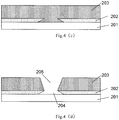
- Fig.4(a) ⁇ Fig.4(b) are flow charts of manufacturing processes of the pixel defining layer according to an embodiment of the present invention.
- the manufacturing method comprises:
- the substrate may be a glass substrate or an array substrate.
- the step 301 may further comprise:
- the negative photoresist film is spin coated or drop coated, the negative photoresist film is exposed and developed so as to form the plurality of first openings 204 corresponding to light-emitting regions of respective sub-pixels in one-to-one correspondence.
- first pixel defining layer 202 is formed by a negative photoresist film
- a cross section of each of the plurality of first openings 204 formed by exposing and developing the first pixel defining layer 202 is in a regular trapezoidal shape which is narrow at top and wide at bottom.
- step 302 forming a hydrophobic film layer on the substrate formed with the first pixel defining layer 202 thereon, as shown in Fig.4(c) , and patterning the hydrophobic film layer to form a second pixel defining layer 203 having a plurality of second openings 205 corresponding to the plurality of first openings 204 in one-to-one correspondence, as shown in Fig.4(d) .
- the step 302 may further comprise:
- the cross section of the formed second opening 205 is in an inverted trapezoidal shape which is wide at top and narrow at bottom.
- the pixel defining layer manufactured by the above manufacturing method proposed in the present invention since both the hydrophilic first pixel defining layer 202 and the hydrophobic the second pixel defining layer 203 are used to constitute the pixel defining layer, and the first pixel defining layer 202 has a plurality of first openings 204 therein corresponding to light-emitting regions of respective sub-pixels in one-to-one correspondence, the second pixel defining layer 203 has a plurality of second openings 205 therein corresponding to the plurality of first openings 204 in one-to-one correspondence.
- the hydrophilic organic light emitting material solution may easily spread in the plurality of first openings 204 in the first pixel defining layer 202 so as to fill the first openings 204, avoiding the short between the anode and the cathode.
- the cross section of the second opening 205 formed therein is in an inverted trapezoidal shape which is wide at top and narrow at bottom, avoiding the open of the cathode.
Landscapes
- Engineering & Computer Science (AREA)
- Physics & Mathematics (AREA)
- Microelectronics & Electronic Packaging (AREA)
- Manufacturing & Machinery (AREA)
- Optics & Photonics (AREA)
- Geometry (AREA)
- Electroluminescent Light Sources (AREA)
Applications Claiming Priority (2)
| Application Number | Priority Date | Filing Date | Title |
|---|---|---|---|
| CN201410736128.4A CN104393192A (zh) | 2014-12-04 | 2014-12-04 | 一种像素界定层及其制作方法、显示面板、显示装置 |
| PCT/CN2015/092262 WO2016086728A1 (zh) | 2014-12-04 | 2015-10-20 | 像素界定层及其制作方法、显示面板和显示装置 |
Publications (3)
| Publication Number | Publication Date |
|---|---|
| EP3229285A1 true EP3229285A1 (de) | 2017-10-11 |
| EP3229285A4 EP3229285A4 (de) | 2018-08-01 |
| EP3229285B1 EP3229285B1 (de) | 2023-07-26 |
Family
ID=52611061
Family Applications (1)
| Application Number | Title | Priority Date | Filing Date |
|---|---|---|---|
| EP15831209.0A Active EP3229285B1 (de) | 2014-12-04 | 2015-10-20 | Anzeigetafel mit pixeldefinitionsschicht |
Country Status (4)
| Country | Link |
|---|---|
| US (1) | US9653526B2 (de) |
| EP (1) | EP3229285B1 (de) |
| CN (1) | CN104393192A (de) |
| WO (1) | WO2016086728A1 (de) |
Cited By (1)
| Publication number | Priority date | Publication date | Assignee | Title |
|---|---|---|---|---|
| CN108110035A (zh) * | 2017-12-14 | 2018-06-01 | 京东方科技集团股份有限公司 | 一种有机发光二极管基板及其制备方法、显示面板 |
Families Citing this family (38)
| Publication number | Priority date | Publication date | Assignee | Title |
|---|---|---|---|---|
| KR102221599B1 (ko) * | 2014-06-18 | 2021-03-02 | 엘지이노텍 주식회사 | 발광 소자 패키지 |
| CN104393192A (zh) * | 2014-12-04 | 2015-03-04 | 京东方科技集团股份有限公司 | 一种像素界定层及其制作方法、显示面板、显示装置 |
| KR102365778B1 (ko) * | 2015-02-24 | 2022-02-21 | 삼성디스플레이 주식회사 | 유기 발광 표시 장치 및 그 제조 방법 |
| CN105206643A (zh) * | 2015-08-21 | 2015-12-30 | Tcl集团股份有限公司 | 一种像素界定层结构及其制作方法、显示面板及显示装置 |
| CN105404038A (zh) * | 2015-12-18 | 2016-03-16 | Tcl集团股份有限公司 | 一种像素界定结构及制作方法、显示面板及显示装置 |
| KR102414593B1 (ko) * | 2015-12-30 | 2022-06-30 | 엘지디스플레이 주식회사 | 유기 발광 표시 장치 및 이의 제조 방법 |
| CN105826355B (zh) * | 2016-05-03 | 2017-03-08 | 京东方科技集团股份有限公司 | 一种显示面板的制作方法 |
| CN107046048B (zh) * | 2016-09-30 | 2020-09-04 | 广东聚华印刷显示技术有限公司 | 像素界定层及其制备方法和应用 |
| CN106783924B (zh) * | 2016-12-27 | 2020-10-27 | Tcl科技集团股份有限公司 | 一种oled显示面板及其制作方法 |
| CN108630828B (zh) * | 2017-03-17 | 2019-11-12 | 昆山工研院新型平板显示技术中心有限公司 | 一种有机电致发光装置及其制备方法 |
| CN107123745B (zh) * | 2017-04-27 | 2018-12-14 | 上海天马有机发光显示技术有限公司 | 像素阵列及其制作方法、显示面板和显示装置 |
| CN109119437B (zh) * | 2017-06-23 | 2021-09-28 | 京东方科技集团股份有限公司 | 像素界定层及制造方法、显示基板及制造方法、显示面板 |
| CN107706317A (zh) * | 2017-09-26 | 2018-02-16 | 京东方科技集团股份有限公司 | 一种oled显示基板的制备方法 |
| CN107706222B (zh) * | 2017-09-28 | 2021-01-22 | 京东方科技集团股份有限公司 | 一种阵列基板及其制备方法、显示面板 |
| CN109994654B (zh) * | 2017-12-29 | 2021-07-16 | 深圳Tcl工业研究院有限公司 | 一种发光器件的制备方法 |
| CN108231856A (zh) * | 2018-01-12 | 2018-06-29 | 京东方科技集团股份有限公司 | 像素界定层、显示面板及显示装置 |
| CN110265428B (zh) * | 2018-03-12 | 2024-05-24 | 京东方科技集团股份有限公司 | 显示面板及其制备方法、显示装置 |
| CN110164906B (zh) * | 2018-03-15 | 2021-03-19 | 合肥视涯技术有限公司 | 一种微型有机发光显示装置及其形成方法 |
| CN108336123B (zh) * | 2018-04-04 | 2021-01-26 | 京东方科技集团股份有限公司 | 一种oled基板及其制备方法、显示装置 |
| CN112038386B (zh) * | 2018-06-19 | 2025-06-27 | 云谷(固安)科技有限公司 | 柔性显示面板及其制备方法和显示装置 |
| CN108987442B (zh) * | 2018-06-29 | 2021-04-30 | 云谷(固安)科技有限公司 | 有机电致发光装置 |
| CN108899349B (zh) * | 2018-07-12 | 2021-01-22 | 京东方科技集团股份有限公司 | 显示面板及其制造方法和显示装置 |
| CN108962964B (zh) * | 2018-08-01 | 2020-06-30 | 京东方科技集团股份有限公司 | 一种显示面板及其制备方法、显示装置 |
| CN109065764B (zh) * | 2018-08-14 | 2023-04-28 | 京东方科技集团股份有限公司 | 显示面板的制造方法及显示面板 |
| CN109346505B (zh) * | 2018-10-11 | 2021-04-13 | 京东方科技集团股份有限公司 | 一种有机发光显示面板、其制备方法及显示装置 |
| CN109509782B (zh) * | 2019-01-02 | 2022-09-16 | 京东方科技集团股份有限公司 | 像素界定层及其制造方法、自发光显示面板、显示装置 |
| CN110047894A (zh) * | 2019-04-24 | 2019-07-23 | 深圳市华星光电半导体显示技术有限公司 | 显示面板及其制作方法 |
| WO2021017011A1 (zh) | 2019-08-01 | 2021-02-04 | 京东方科技集团股份有限公司 | 显示基板及显示装置 |
| CN112420967A (zh) * | 2019-08-21 | 2021-02-26 | 咸阳彩虹光电科技有限公司 | 一种显示面板的制备方法、显示面板及显示装置 |
| CN112420968B (zh) * | 2019-08-21 | 2023-02-03 | 咸阳彩虹光电科技有限公司 | 一种显示面板的制造方法、显示面板及显示装置 |
| CN110854169A (zh) * | 2019-10-31 | 2020-02-28 | 深圳市华星光电半导体显示技术有限公司 | 一种oled器件及其制备方法 |
| CN111092111A (zh) * | 2020-01-16 | 2020-05-01 | 云谷(固安)科技有限公司 | 显示面板、显示面板的制备方法以及显示装置 |
| CN111370586A (zh) * | 2020-03-18 | 2020-07-03 | 昆山国显光电有限公司 | 显示面板及其制备方法、显示装置 |
| CN113571545A (zh) * | 2020-04-28 | 2021-10-29 | 海信视像科技股份有限公司 | 一种显示装置及其制作方法 |
| CN111564484A (zh) * | 2020-05-22 | 2020-08-21 | 云谷(固安)科技有限公司 | 显示面板以其加工方法、显示装置 |
| US12302710B2 (en) | 2021-08-11 | 2025-05-13 | Yunnan Invensight Optoelectronics Technology Co., Ltd. | Display substrate and electronic apparatus |
| WO2023015488A1 (zh) | 2021-08-11 | 2023-02-16 | 京东方科技集团股份有限公司 | 显示基板及电子装置 |
| CN115832121B (zh) * | 2022-10-11 | 2026-02-24 | 京东方华灿光电(苏州)有限公司 | 改善电极包覆性的发光二极管及其制备方法 |
Family Cites Families (13)
| Publication number | Priority date | Publication date | Assignee | Title |
|---|---|---|---|---|
| JP2003007460A (ja) | 2001-06-22 | 2003-01-10 | Sony Corp | 表示装置の製造方法および表示装置 |
| JP3858707B2 (ja) * | 2002-01-29 | 2006-12-20 | 株式会社豊田自動織機 | 有機el素子 |
| JP3915806B2 (ja) * | 2003-11-11 | 2007-05-16 | セイコーエプソン株式会社 | 電気光学装置および電子機器 |
| JP5092485B2 (ja) * | 2007-03-27 | 2012-12-05 | 凸版印刷株式会社 | 有機エレクトロルミネッセンスディスプレイ及びその製造方法 |
| GB2455747B (en) * | 2007-12-19 | 2011-02-09 | Cambridge Display Tech Ltd | Electronic devices and methods of making the same using solution processing techniques |
| KR101073561B1 (ko) * | 2009-02-05 | 2011-10-17 | 삼성모바일디스플레이주식회사 | 유기전계발광소자 및 그의 제조 방법 |
| CN102945855B (zh) * | 2012-11-13 | 2016-08-03 | 京东方科技集团股份有限公司 | 发光显示背板、显示装置和像素界定层的制备方法 |
| KR102097443B1 (ko) * | 2013-05-09 | 2020-04-07 | 삼성디스플레이 주식회사 | 유기 발광 표시 장치 및 그 제조 방법 |
| CN103413819B (zh) * | 2013-07-22 | 2016-08-31 | 京东方科技集团股份有限公司 | 一种有机发光显示面板、像素界定层及其制作方法 |
| KR102280777B1 (ko) * | 2013-12-20 | 2021-07-23 | 삼성디스플레이 주식회사 | 표시 장치 및 그 제조 방법 |
| CN103928497B (zh) * | 2014-04-01 | 2016-07-13 | 京东方科技集团股份有限公司 | Oled显示器件及其制作方法、显示装置 |
| CN203787433U (zh) * | 2014-04-01 | 2014-08-20 | 京东方科技集团股份有限公司 | Oled显示器件及显示装置 |
| CN104393192A (zh) * | 2014-12-04 | 2015-03-04 | 京东方科技集团股份有限公司 | 一种像素界定层及其制作方法、显示面板、显示装置 |
-
2014
- 2014-12-04 CN CN201410736128.4A patent/CN104393192A/zh active Pending
-
2015
- 2015-10-20 EP EP15831209.0A patent/EP3229285B1/de active Active
- 2015-10-20 WO PCT/CN2015/092262 patent/WO2016086728A1/zh not_active Ceased
- 2015-10-20 US US14/912,267 patent/US9653526B2/en not_active Expired - Fee Related
Cited By (2)
| Publication number | Priority date | Publication date | Assignee | Title |
|---|---|---|---|---|
| CN108110035A (zh) * | 2017-12-14 | 2018-06-01 | 京东方科技集团股份有限公司 | 一种有机发光二极管基板及其制备方法、显示面板 |
| CN108110035B (zh) * | 2017-12-14 | 2020-11-27 | 京东方科技集团股份有限公司 | 一种有机发光二极管基板及其制备方法、显示面板 |
Also Published As
| Publication number | Publication date |
|---|---|
| US9653526B2 (en) | 2017-05-16 |
| US20160351635A1 (en) | 2016-12-01 |
| EP3229285B1 (de) | 2023-07-26 |
| EP3229285A4 (de) | 2018-08-01 |
| WO2016086728A1 (zh) | 2016-06-09 |
| CN104393192A (zh) | 2015-03-04 |
Similar Documents
| Publication | Publication Date | Title |
|---|---|---|
| US9653526B2 (en) | Pixel defining layer and manufacturing method thereof, display panel and display device | |
| US10886343B2 (en) | Pixel defining layer and method for manufacturing the same, display panel and method for manufacturing the same, and display device | |
| US10403819B2 (en) | Pixel define layer and manufacturing method thereof and related light emitting display | |
| US9224975B2 (en) | Organic light emitting display panel and method of manufacturing the same | |
| US10283576B2 (en) | Organic light emitting display substrate in which light emitted from light emitting unit has increased uniformity, manufacturing method thereof and display device | |
| EP3240029B1 (de) | Anzeigesubstrat, herstellungsverfahren und anzeigevorrichtung dafür | |
| US11276735B2 (en) | Array substrate, method of fabricating array substrate, display panel, and display device | |
| US10163993B2 (en) | Display panel and method for manufacturing same | |
| CN107819017B (zh) | 像素界定结构、显示基板及其制作方法和显示装置 | |
| US11088211B2 (en) | Display substrate, manufacturing method thereof, and display apparatus | |
| US10305049B2 (en) | OLED substrate and manufacture method thereof | |
| US11239282B2 (en) | Pixel structure and fabrication method thereof, display substrate and display apparatus | |
| CN108565352B (zh) | 有机发光二极管显示面板及其制造方法、显示装置 | |
| CN103413819A (zh) | 一种有机发光显示面板、像素界定层及其制作方法 | |
| JP2019504434A (ja) | タッチスクリーンとその製造方法及び表示装置 | |
| CN110137225A (zh) | Oled显示面板及其制备方法 | |
| CN111584553A (zh) | Oled像素排布结构、oled显示面板及显示面板的制作方法 | |
| CN108400153A (zh) | 一种oled基板及其制备方法、显示装置 | |
| US20170125486A1 (en) | Pixel unit and method for fabricating the same, display device | |
| CN107204358A (zh) | 像素结构 | |
| US11889739B2 (en) | OLED with electron transport layer within insulating layer | |
| CN111312750A (zh) | 像素排布结构、oled显示面板及其制备方法 | |
| US20260136768A1 (en) | Display panel, method for manufacturing same, and display device | |
| JP2013020711A (ja) | 有機el装置の製造方法 | |
| JP2008159445A (ja) | 有機電界発光表示装置及びその製造方法 |
Legal Events
| Date | Code | Title | Description |
|---|---|---|---|
| STAA | Information on the status of an ep patent application or granted ep patent |
Free format text: STATUS: THE INTERNATIONAL PUBLICATION HAS BEEN MADE |
|
| PUAI | Public reference made under article 153(3) epc to a published international application that has entered the european phase |
Free format text: ORIGINAL CODE: 0009012 |
|
| STAA | Information on the status of an ep patent application or granted ep patent |
Free format text: STATUS: REQUEST FOR EXAMINATION WAS MADE |
|
| 17P | Request for examination filed |
Effective date: 20160218 |
|
| AK | Designated contracting states |
Kind code of ref document: A1 Designated state(s): AL AT BE BG CH CY CZ DE DK EE ES FI FR GB GR HR HU IE IS IT LI LT LU LV MC MK MT NL NO PL PT RO RS SE SI SK SM TR |
|
| AX | Request for extension of the european patent |
Extension state: BA ME |
|
| DAV | Request for validation of the european patent (deleted) | ||
| DAX | Request for extension of the european patent (deleted) | ||
| A4 | Supplementary search report drawn up and despatched |
Effective date: 20180704 |
|
| RIC1 | Information provided on ipc code assigned before grant |
Ipc: H01L 51/52 20060101AFI20180628BHEP Ipc: H01L 27/32 20060101ALI20180628BHEP Ipc: H01L 51/56 20060101ALI20180628BHEP |
|
| STAA | Information on the status of an ep patent application or granted ep patent |
Free format text: STATUS: EXAMINATION IS IN PROGRESS |
|
| 17Q | First examination report despatched |
Effective date: 20210330 |
|
| REG | Reference to a national code |
Ref country code: DE Ref legal event code: R079 Free format text: PREVIOUS MAIN CLASS: H01L0051520000 Ipc: H10K0059122000 Ref document number: 602015084806 Country of ref document: DE |
|
| RIC1 | Information provided on ipc code assigned before grant |
Ipc: H10K 59/122 20230101AFI20230125BHEP |
|
| GRAP | Despatch of communication of intention to grant a patent |
Free format text: ORIGINAL CODE: EPIDOSNIGR1 |
|
| STAA | Information on the status of an ep patent application or granted ep patent |
Free format text: STATUS: GRANT OF PATENT IS INTENDED |
|
| INTG | Intention to grant announced |
Effective date: 20230317 |
|
| GRAS | Grant fee paid |
Free format text: ORIGINAL CODE: EPIDOSNIGR3 |
|
| GRAA | (expected) grant |
Free format text: ORIGINAL CODE: 0009210 |
|
| STAA | Information on the status of an ep patent application or granted ep patent |
Free format text: STATUS: THE PATENT HAS BEEN GRANTED |
|
| AK | Designated contracting states |
Kind code of ref document: B1 Designated state(s): AL AT BE BG CH CY CZ DE DK EE ES FI FR GB GR HR HU IE IS IT LI LT LU LV MC MK MT NL NO PL PT RO RS SE SI SK SM TR |
|
| REG | Reference to a national code |
Ref country code: GB Ref legal event code: FG4D |
|
| REG | Reference to a national code |
Ref country code: CH Ref legal event code: EP |
|
| REG | Reference to a national code |
Ref country code: IE Ref legal event code: FG4D |
|
| REG | Reference to a national code |
Ref country code: DE Ref legal event code: R096 Ref document number: 602015084806 Country of ref document: DE |
|
| REG | Reference to a national code |
Ref country code: LT Ref legal event code: MG9D |
|
| REG | Reference to a national code |
Ref country code: NL Ref legal event code: MP Effective date: 20230726 |
|
| REG | Reference to a national code |
Ref country code: AT Ref legal event code: MK05 Ref document number: 1593498 Country of ref document: AT Kind code of ref document: T Effective date: 20230726 |
|
| PG25 | Lapsed in a contracting state [announced via postgrant information from national office to epo] |
Ref country code: NL Free format text: LAPSE BECAUSE OF FAILURE TO SUBMIT A TRANSLATION OF THE DESCRIPTION OR TO PAY THE FEE WITHIN THE PRESCRIBED TIME-LIMIT Effective date: 20230726 |
|
| PG25 | Lapsed in a contracting state [announced via postgrant information from national office to epo] |
Ref country code: GR Free format text: LAPSE BECAUSE OF FAILURE TO SUBMIT A TRANSLATION OF THE DESCRIPTION OR TO PAY THE FEE WITHIN THE PRESCRIBED TIME-LIMIT Effective date: 20231027 |
|
| PG25 | Lapsed in a contracting state [announced via postgrant information from national office to epo] |
Ref country code: IS Free format text: LAPSE BECAUSE OF FAILURE TO SUBMIT A TRANSLATION OF THE DESCRIPTION OR TO PAY THE FEE WITHIN THE PRESCRIBED TIME-LIMIT Effective date: 20231126 |
|
| PG25 | Lapsed in a contracting state [announced via postgrant information from national office to epo] |
Ref country code: SE Free format text: LAPSE BECAUSE OF FAILURE TO SUBMIT A TRANSLATION OF THE DESCRIPTION OR TO PAY THE FEE WITHIN THE PRESCRIBED TIME-LIMIT Effective date: 20230726 Ref country code: RS Free format text: LAPSE BECAUSE OF FAILURE TO SUBMIT A TRANSLATION OF THE DESCRIPTION OR TO PAY THE FEE WITHIN THE PRESCRIBED TIME-LIMIT Effective date: 20230726 Ref country code: PT Free format text: LAPSE BECAUSE OF FAILURE TO SUBMIT A TRANSLATION OF THE DESCRIPTION OR TO PAY THE FEE WITHIN THE PRESCRIBED TIME-LIMIT Effective date: 20231127 Ref country code: NO Free format text: LAPSE BECAUSE OF FAILURE TO SUBMIT A TRANSLATION OF THE DESCRIPTION OR TO PAY THE FEE WITHIN THE PRESCRIBED TIME-LIMIT Effective date: 20231026 Ref country code: LV Free format text: LAPSE BECAUSE OF FAILURE TO SUBMIT A TRANSLATION OF THE DESCRIPTION OR TO PAY THE FEE WITHIN THE PRESCRIBED TIME-LIMIT Effective date: 20230726 Ref country code: LT Free format text: LAPSE BECAUSE OF FAILURE TO SUBMIT A TRANSLATION OF THE DESCRIPTION OR TO PAY THE FEE WITHIN THE PRESCRIBED TIME-LIMIT Effective date: 20230726 Ref country code: IS Free format text: LAPSE BECAUSE OF FAILURE TO SUBMIT A TRANSLATION OF THE DESCRIPTION OR TO PAY THE FEE WITHIN THE PRESCRIBED TIME-LIMIT Effective date: 20231126 Ref country code: HR Free format text: LAPSE BECAUSE OF FAILURE TO SUBMIT A TRANSLATION OF THE DESCRIPTION OR TO PAY THE FEE WITHIN THE PRESCRIBED TIME-LIMIT Effective date: 20230726 Ref country code: GR Free format text: LAPSE BECAUSE OF FAILURE TO SUBMIT A TRANSLATION OF THE DESCRIPTION OR TO PAY THE FEE WITHIN THE PRESCRIBED TIME-LIMIT Effective date: 20231027 Ref country code: FI Free format text: LAPSE BECAUSE OF FAILURE TO SUBMIT A TRANSLATION OF THE DESCRIPTION OR TO PAY THE FEE WITHIN THE PRESCRIBED TIME-LIMIT Effective date: 20230726 Ref country code: AT Free format text: LAPSE BECAUSE OF FAILURE TO SUBMIT A TRANSLATION OF THE DESCRIPTION OR TO PAY THE FEE WITHIN THE PRESCRIBED TIME-LIMIT Effective date: 20230726 |
|
| PG25 | Lapsed in a contracting state [announced via postgrant information from national office to epo] |
Ref country code: PL Free format text: LAPSE BECAUSE OF FAILURE TO SUBMIT A TRANSLATION OF THE DESCRIPTION OR TO PAY THE FEE WITHIN THE PRESCRIBED TIME-LIMIT Effective date: 20230726 |
|
| PG25 | Lapsed in a contracting state [announced via postgrant information from national office to epo] |
Ref country code: ES Free format text: LAPSE BECAUSE OF FAILURE TO SUBMIT A TRANSLATION OF THE DESCRIPTION OR TO PAY THE FEE WITHIN THE PRESCRIBED TIME-LIMIT Effective date: 20230726 |
|
| REG | Reference to a national code |
Ref country code: DE Ref legal event code: R097 Ref document number: 602015084806 Country of ref document: DE |
|
| PG25 | Lapsed in a contracting state [announced via postgrant information from national office to epo] |
Ref country code: SM Free format text: LAPSE BECAUSE OF FAILURE TO SUBMIT A TRANSLATION OF THE DESCRIPTION OR TO PAY THE FEE WITHIN THE PRESCRIBED TIME-LIMIT Effective date: 20230726 Ref country code: RO Free format text: LAPSE BECAUSE OF FAILURE TO SUBMIT A TRANSLATION OF THE DESCRIPTION OR TO PAY THE FEE WITHIN THE PRESCRIBED TIME-LIMIT Effective date: 20230726 Ref country code: ES Free format text: LAPSE BECAUSE OF FAILURE TO SUBMIT A TRANSLATION OF THE DESCRIPTION OR TO PAY THE FEE WITHIN THE PRESCRIBED TIME-LIMIT Effective date: 20230726 Ref country code: EE Free format text: LAPSE BECAUSE OF FAILURE TO SUBMIT A TRANSLATION OF THE DESCRIPTION OR TO PAY THE FEE WITHIN THE PRESCRIBED TIME-LIMIT Effective date: 20230726 Ref country code: DK Free format text: LAPSE BECAUSE OF FAILURE TO SUBMIT A TRANSLATION OF THE DESCRIPTION OR TO PAY THE FEE WITHIN THE PRESCRIBED TIME-LIMIT Effective date: 20230726 Ref country code: CZ Free format text: LAPSE BECAUSE OF FAILURE TO SUBMIT A TRANSLATION OF THE DESCRIPTION OR TO PAY THE FEE WITHIN THE PRESCRIBED TIME-LIMIT Effective date: 20230726 Ref country code: SK Free format text: LAPSE BECAUSE OF FAILURE TO SUBMIT A TRANSLATION OF THE DESCRIPTION OR TO PAY THE FEE WITHIN THE PRESCRIBED TIME-LIMIT Effective date: 20230726 |
|
| PG25 | Lapsed in a contracting state [announced via postgrant information from national office to epo] |
Ref country code: IT Free format text: LAPSE BECAUSE OF FAILURE TO SUBMIT A TRANSLATION OF THE DESCRIPTION OR TO PAY THE FEE WITHIN THE PRESCRIBED TIME-LIMIT Effective date: 20230726 Ref country code: MC Free format text: LAPSE BECAUSE OF FAILURE TO SUBMIT A TRANSLATION OF THE DESCRIPTION OR TO PAY THE FEE WITHIN THE PRESCRIBED TIME-LIMIT Effective date: 20230726 |
|
| PLBE | No opposition filed within time limit |
Free format text: ORIGINAL CODE: 0009261 |
|
| REG | Reference to a national code |
Ref country code: CH Ref legal event code: PL |
|
| STAA | Information on the status of an ep patent application or granted ep patent |
Free format text: STATUS: NO OPPOSITION FILED WITHIN TIME LIMIT |
|
| REG | Reference to a national code |
Ref country code: BE Ref legal event code: MM Effective date: 20231031 |
|
| PG25 | Lapsed in a contracting state [announced via postgrant information from national office to epo] |
Ref country code: LU Free format text: LAPSE BECAUSE OF NON-PAYMENT OF DUE FEES Effective date: 20231020 |
|
| GBPC | Gb: european patent ceased through non-payment of renewal fee |
Effective date: 20231026 |
|
| PG25 | Lapsed in a contracting state [announced via postgrant information from national office to epo] |
Ref country code: LU Free format text: LAPSE BECAUSE OF NON-PAYMENT OF DUE FEES Effective date: 20231020 |
|
| 26N | No opposition filed |
Effective date: 20240429 |
|
| PG25 | Lapsed in a contracting state [announced via postgrant information from national office to epo] |
Ref country code: GB Free format text: LAPSE BECAUSE OF NON-PAYMENT OF DUE FEES Effective date: 20231026 |
|
| PG25 | Lapsed in a contracting state [announced via postgrant information from national office to epo] |
Ref country code: CH Free format text: LAPSE BECAUSE OF NON-PAYMENT OF DUE FEES Effective date: 20231031 |
|
| PG25 | Lapsed in a contracting state [announced via postgrant information from national office to epo] |
Ref country code: GB Free format text: LAPSE BECAUSE OF NON-PAYMENT OF DUE FEES Effective date: 20231026 Ref country code: FR Free format text: LAPSE BECAUSE OF NON-PAYMENT OF DUE FEES Effective date: 20231031 Ref country code: CH Free format text: LAPSE BECAUSE OF NON-PAYMENT OF DUE FEES Effective date: 20231031 Ref country code: SI Free format text: LAPSE BECAUSE OF FAILURE TO SUBMIT A TRANSLATION OF THE DESCRIPTION OR TO PAY THE FEE WITHIN THE PRESCRIBED TIME-LIMIT Effective date: 20230726 |
|
| PG25 | Lapsed in a contracting state [announced via postgrant information from national office to epo] |
Ref country code: BE Free format text: LAPSE BECAUSE OF NON-PAYMENT OF DUE FEES Effective date: 20231031 |
|
| PG25 | Lapsed in a contracting state [announced via postgrant information from national office to epo] |
Ref country code: IE Free format text: LAPSE BECAUSE OF NON-PAYMENT OF DUE FEES Effective date: 20231020 |
|
| PG25 | Lapsed in a contracting state [announced via postgrant information from national office to epo] |
Ref country code: IE Free format text: LAPSE BECAUSE OF NON-PAYMENT OF DUE FEES Effective date: 20231020 |
|
| PG25 | Lapsed in a contracting state [announced via postgrant information from national office to epo] |
Ref country code: BG Free format text: LAPSE BECAUSE OF FAILURE TO SUBMIT A TRANSLATION OF THE DESCRIPTION OR TO PAY THE FEE WITHIN THE PRESCRIBED TIME-LIMIT Effective date: 20230726 |
|
| PG25 | Lapsed in a contracting state [announced via postgrant information from national office to epo] |
Ref country code: BG Free format text: LAPSE BECAUSE OF FAILURE TO SUBMIT A TRANSLATION OF THE DESCRIPTION OR TO PAY THE FEE WITHIN THE PRESCRIBED TIME-LIMIT Effective date: 20230726 |
|
| PGFP | Annual fee paid to national office [announced via postgrant information from national office to epo] |
Ref country code: DE Payment date: 20241021 Year of fee payment: 10 |
|
| PG25 | Lapsed in a contracting state [announced via postgrant information from national office to epo] |
Ref country code: CY Free format text: LAPSE BECAUSE OF FAILURE TO SUBMIT A TRANSLATION OF THE DESCRIPTION OR TO PAY THE FEE WITHIN THE PRESCRIBED TIME-LIMIT; INVALID AB INITIO Effective date: 20151020 |
|
| PG25 | Lapsed in a contracting state [announced via postgrant information from national office to epo] |
Ref country code: HU Free format text: LAPSE BECAUSE OF FAILURE TO SUBMIT A TRANSLATION OF THE DESCRIPTION OR TO PAY THE FEE WITHIN THE PRESCRIBED TIME-LIMIT; INVALID AB INITIO Effective date: 20151020 |
|
| PG25 | Lapsed in a contracting state [announced via postgrant information from national office to epo] |
Ref country code: TR Free format text: LAPSE BECAUSE OF FAILURE TO SUBMIT A TRANSLATION OF THE DESCRIPTION OR TO PAY THE FEE WITHIN THE PRESCRIBED TIME-LIMIT Effective date: 20230726 |