EP3231090B1 - Geregelte spannungsseitige gatetreiberschaltung für leistungstransistoren - Google Patents
Geregelte spannungsseitige gatetreiberschaltung für leistungstransistoren Download PDFInfo
- Publication number
- EP3231090B1 EP3231090B1 EP15802043.8A EP15802043A EP3231090B1 EP 3231090 B1 EP3231090 B1 EP 3231090B1 EP 15802043 A EP15802043 A EP 15802043A EP 3231090 B1 EP3231090 B1 EP 3231090B1
- Authority
- EP
- European Patent Office
- Prior art keywords
- voltage
- gate driver
- high side
- regulated
- output
- Prior art date
- Legal status (The legal status is an assumption and is not a legal conclusion. Google has not performed a legal analysis and makes no representation as to the accuracy of the status listed.)
- Active
Links
Images



Classifications
-
- H—ELECTRICITY
- H02—GENERATION; CONVERSION OR DISTRIBUTION OF ELECTRIC POWER
- H02M—APPARATUS FOR CONVERSION BETWEEN AC AND AC, BETWEEN AC AND DC, OR BETWEEN DC AND DC, AND FOR USE WITH MAINS OR SIMILAR POWER SUPPLY SYSTEMS; CONVERSION OF DC OR AC INPUT POWER INTO SURGE OUTPUT POWER; CONTROL OR REGULATION THEREOF
- H02M1/00—Details of apparatus for conversion
- H02M1/08—Circuits specially adapted for the generation of control voltages for semiconductor devices incorporated in static converters
-
- H—ELECTRICITY
- H03—ELECTRONIC CIRCUITRY
- H03F—AMPLIFIERS
- H03F3/00—Amplifiers with only discharge tubes or only semiconductor devices as amplifying elements
- H03F3/20—Power amplifiers, e.g. Class B amplifiers, Class C amplifiers
- H03F3/21—Power amplifiers, e.g. Class B amplifiers, Class C amplifiers with semiconductor devices only
- H03F3/217—Class D power amplifiers; Switching amplifiers
- H03F3/2173—Class D power amplifiers; Switching amplifiers of the bridge type
-
- H—ELECTRICITY
- H10—SEMICONDUCTOR DEVICES; ELECTRIC SOLID-STATE DEVICES NOT OTHERWISE PROVIDED FOR
- H10D—INORGANIC ELECTRIC SEMICONDUCTOR DEVICES
- H10D84/00—Integrated devices formed in or on semiconductor substrates that comprise only semiconducting layers, e.g. on Si wafers or on GaAs-on-Si wafers
- H10D84/01—Manufacture or treatment
- H10D84/0123—Integrating together multiple components covered by H10D12/00 or H10D30/00, e.g. integrating multiple IGBTs
- H10D84/0126—Integrating together multiple components covered by H10D12/00 or H10D30/00, e.g. integrating multiple IGBTs the components including insulated gates, e.g. IGFETs
- H10D84/0165—Integrating together multiple components covered by H10D12/00 or H10D30/00, e.g. integrating multiple IGBTs the components including insulated gates, e.g. IGFETs the components including complementary IGFETs, e.g. CMOS devices
- H10D84/0191—Manufacturing their doped wells
-
- H—ELECTRICITY
- H10—SEMICONDUCTOR DEVICES; ELECTRIC SOLID-STATE DEVICES NOT OTHERWISE PROVIDED FOR
- H10D—INORGANIC ELECTRIC SEMICONDUCTOR DEVICES
- H10D84/00—Integrated devices formed in or on semiconductor substrates that comprise only semiconducting layers, e.g. on Si wafers or on GaAs-on-Si wafers
- H10D84/01—Manufacture or treatment
- H10D84/02—Manufacture or treatment characterised by using material-based technologies
- H10D84/03—Manufacture or treatment characterised by using material-based technologies using Group IV technology, e.g. silicon technology or silicon-carbide [SiC] technology
- H10D84/038—Manufacture or treatment characterised by using material-based technologies using Group IV technology, e.g. silicon technology or silicon-carbide [SiC] technology using silicon technology, e.g. SiGe
-
- H—ELECTRICITY
- H10—SEMICONDUCTOR DEVICES; ELECTRIC SOLID-STATE DEVICES NOT OTHERWISE PROVIDED FOR
- H10D—INORGANIC ELECTRIC SEMICONDUCTOR DEVICES
- H10D84/00—Integrated devices formed in or on semiconductor substrates that comprise only semiconducting layers, e.g. on Si wafers or on GaAs-on-Si wafers
- H10D84/80—Integrated devices formed in or on semiconductor substrates that comprise only semiconducting layers, e.g. on Si wafers or on GaAs-on-Si wafers characterised by the integration of at least one component covered by groups H10D12/00 or H10D30/00, e.g. integration of IGFETs
- H10D84/82—Integrated devices formed in or on semiconductor substrates that comprise only semiconducting layers, e.g. on Si wafers or on GaAs-on-Si wafers characterised by the integration of at least one component covered by groups H10D12/00 or H10D30/00, e.g. integration of IGFETs of only field-effect components
- H10D84/83—Integrated devices formed in or on semiconductor substrates that comprise only semiconducting layers, e.g. on Si wafers or on GaAs-on-Si wafers characterised by the integration of at least one component covered by groups H10D12/00 or H10D30/00, e.g. integration of IGFETs of only field-effect components of only insulated-gate FETs [IGFET]
- H10D84/85—Complementary IGFETs, e.g. CMOS
-
- H—ELECTRICITY
- H10—SEMICONDUCTOR DEVICES; ELECTRIC SOLID-STATE DEVICES NOT OTHERWISE PROVIDED FOR
- H10W—GENERIC PACKAGES, INTERCONNECTIONS, CONNECTORS OR OTHER CONSTRUCTIONAL DETAILS OF DEVICES COVERED BY CLASS H10
- H10W10/00—Isolation regions in semiconductor bodies between components of integrated devices
- H10W10/01—Manufacture or treatment
- H10W10/031—Manufacture or treatment of isolation regions comprising PN junctions
-
- H—ELECTRICITY
- H10—SEMICONDUCTOR DEVICES; ELECTRIC SOLID-STATE DEVICES NOT OTHERWISE PROVIDED FOR
- H10W—GENERIC PACKAGES, INTERCONNECTIONS, CONNECTORS OR OTHER CONSTRUCTIONAL DETAILS OF DEVICES COVERED BY CLASS H10
- H10W10/00—Isolation regions in semiconductor bodies between components of integrated devices
- H10W10/30—Isolation regions comprising PN junctions
-
- H—ELECTRICITY
- H03—ELECTRONIC CIRCUITRY
- H03K—PULSE TECHNIQUE
- H03K2217/00—Indexing scheme related to electronic switching or gating, i.e. not by contact-making or -breaking covered by H03K17/00
- H03K2217/0063—High side switches, i.e. the higher potential [DC] or life wire [AC] being directly connected to the switch and not via the load
-
- H—ELECTRICITY
- H03—ELECTRONIC CIRCUITRY
- H03K—PULSE TECHNIQUE
- H03K2217/00—Indexing scheme related to electronic switching or gating, i.e. not by contact-making or -breaking covered by H03K17/00
- H03K2217/0081—Power supply means, e.g. to the switch driver
Definitions
- the present invention relates in a first aspect to a regulated high side gate driver circuit for power transistors.
- the regulated high side gate driver circuit comprises a gate driver powered by a floating voltage regulator which comprises a linear regulating device.
- CMOS and DMOS high voltage semiconductor processes are typical candidates for implementation of these integrated class D audio amplifiers which feature large LDMOS output devices as active switches of output stages. These LDMOS transistors are isolated high side devices and typically NMOS devices to minimize transistor dimensions for a given output resistance of the output stage. As the bipolar CMOS and DMOS high voltage semiconductor processes continue to evolve to feature sizes at 180 nm and below, the gate drive voltage required to the LDMOS active switches is approaching a voltage level around 5 V.
- This gate drive voltage should not be exceeded by the high side gate driver to maintain gate integrity by limiting the gate-source voltage of the high side LDMOS transistor to a voltage range that fits an oxide voltage range of the LDMOS transistor in question, such as the above-mentioned maximum of 5 V.
- This drive voltage accuracy requirement or constraint complicates the design of an adequate DC power supply voltage, i.e. the high side positive supply voltage, to the high side gate driver.
- the accuracy and stability requirements of the gate-source voltage applied to the high side LDMOS transistor have been accomplished by using an external bootstrap capacitor for the DC supply voltage of the high gate driver of every high side LDMOS transistor.
- a typical Class D audio amplifier may include numerous high side power transistors and associated high side gate driver circuits each needing an external capacitor. This is for example the situation for H-bridge configured output stages of multi-level PWM amplifiers.
- WO 2012/005341 A1 describes a driving circuit which includes a switching element configured to be connected between an input terminal and an output node; a first power supply circuit configured to generate a first voltage; and a first driving circuit configured to drive the switching element with an output thereof using a voltage of the output node as a reference negative-side power supply voltage and the first voltage as a positive-side power supply voltage.
- the voltage of the output node is used as a reference negative-side power supply voltage of the first power supply.
- the present regulated high side gate driver circuit which comprises a novel type of a floating voltage regulator design providing an accurate and stable regulated supply voltage to the gate driver.
- a first aspect of invention relates to a regulated high side gate driver circuit for power transistors according to claim 1.
- the floating voltage regulator is connected to the high side positive and negative supply voltage ports of the gate driver and therefore able to maintain an accurate supply voltage level to the gate driver despite voltage fluctuations and voltage spikes on the high side DC voltage supply.
- the voltage swing delivered at the driver output of the gate driver may be limited or restricted to a voltage range that fits the previously discussed oxide voltage range of the power transistor connected to the driver output of the gate driver.
- the DC voltage of the regulated DC voltage output preferably is substantially constant, referred to the negative regulator input, It may be secured that the drive voltage of the gate driver never exceeds the maximum safe gate voltage of the power transistor coupled to the driver output of the gate driver.
- the DC voltage of the regulated DC voltage output may be set by a suitable programming, adjustment or design of the DC reference voltage generator. The skilled person will understand that the DC voltage of the regulated DC voltage output preferably is substantially constant referred to the negative regulator input.
- the linear regulating device may comprise a transistor arrangement comprising one or more transistors such as MOS or LDMOS transistors.
- the term linear means in the present context that the regulating device is non-switched and the voltage drop across the regulating device produces the predetermined regulated DC voltage.
- the gate driver may comprise an inverter topology transistor driver.
- the inverter topology transistor driver may comprise first and second cascaded transistors between the high side positive and negative supply voltage ports of the gate driver. Respective drain or emitter terminals of the series connected first and second transistors are connected to the driver output.
- the control terminals of the first and second transistors are preferably interconnected to form a common control terminal of the transistor driver.
- the connection of the regulation capacitor between the positive and negative terminals of the DC reference voltage generator reduces the capacitance requirement to a sufficiently small value to allow integration of the regulation capacitor on a semiconductor substrate without incurring unacceptable die area consumption.
- the capacitance of the regulation capacitor may for example be smaller than 200 pF, or more preferably smaller than 100 pF.
- the regulation capacitor comprises a metal-insulator-metal (MIM) capacitor with the advantages discussed in further detail below.
- the MIM capacitor may have a capacitance between 1 pF and 1 00 pF such as between 10 pF and 50 pF.
- the floating voltage regulator comprises an open-loop topology or feed-forward topology.
- These embodiments accordingly lack a voltage or current regulation feedback loop extending from the regulated DC voltage output back to the control terminal of the linear regulating device.
- the open-loop or feed-forward topology of the floating voltage regulator provides a fast response time to the regularly encountered extremely rapid load changes at the regulated DC voltage output.
- the open-loop or feed-forward topology therefore enables accurate load regulation at the regulated DC voltage output even under challenging load variations as discussed in further detail below in connection with the appended drawings.
- the linear regulating may device comprise a pass transistor connected between the positive regulator input and the regulated DC voltage output, wherein a control terminal of the pass transistor is connected to the DC reference voltage generated by the DC reference voltage generator.
- the pass transistor may comprises MOSFET or bipolar transistor with a source or emitter, respectively, connected to the regulated DC voltage output, and a drain or collector terminal, respectively, connected to the positive regulator input.
- the linear regulating device comprises a class AB output stage having a positive power supply terminal connected to the positive regulator input and a negative power supply terminal connected to the negative regulator input.
- a control terminal of the class AB output stage is furthermore connected to the DC reference voltage and an output of the class AB output stage is coupled to the regulated DC voltage output to source current out, or sink current from, the load at the regulated DC voltage output.
- the class AB output stage is capable of both sourcing current out of, and sinking current into, the regulated DC voltage output. This feature may lead to a more effective suppression of high-frequency ac ripple or noise voltages appearing on the regulated DC voltage output.
- the class AB output stage comprises a first output transistor connected between the positive regulator input and the regulated DC voltage output, a second output transistor connected between the negative regulator input and the regulated DC voltage output; and a bias voltage circuit connected between respective control terminals of the first and second output transistors to set a predetermined DC bias current therein.
- the DC reference voltage generator comprises a reversely biased Zener diode, i.e. a Zener diode biased in reverse breakdown mode.
- the Zener diode is preferably connected between the DC reference voltage and the negative regulator input.
- a constant current generator may be configured apply a predetermined DC bias current to a cathode of the Zener diode to develop a suitable, and relatively stable, DC voltage drop across the Zener diode.
- An alternative embodiment of the DC reference voltage generator comprises a shunt regulator circuit.
- the shunt regulator circuit may comprise a shunt transistor connected between the DC reference voltage and the negative regulator input and an error amplifier where the latter comprises an output, a first input and a second input.
- the output of the error amplifier is connected to a control terminal of the shunt transistor.
- the shunt regulator circuit further comprises a voltage divider connected to the DC reference voltage and configured to supply a shunt voltage proportional to the DC reference voltage to the first input of the error amplifier.
- a second DC voltage reference connected to the second input of the error amplifier.
- the shunt transistor may comprise a drain extended NMOS (DE-NMOS) transistor in which a first drain terminal of the drain extended NMOS transistor is connected to the DC reference voltage and a second, or extended, drain terminal is connected to the regulated DC voltage output.
- DE-NMOS drain extended NMOS
- the floating voltage regulator may be configured to provide a DC voltage level at the regulated DC voltage output which is at least 5 V higher than a DC voltage supply of the power transistor coupled to the gate driver of the regulated high side gate driver circuit.
- the power transistor may form part of a class D audio amplifier output stage which comprises a plurality of stacked power transistors as discussed below in further detail.
- the overdrive capability of at least 5 V of the gate driver ensures an NMOS power transistor of the output stage can be driven into an appropriate low impedance on-state.
- a DC voltage of the high side DC voltage supply of the regulated high side gate driver circuit may be at least 2 V higher than the DC voltage level of the regulated DC voltage output to ensure that the linear regulating device, e.g.
- the pass transistor may comprise a LDNMOS or LDPMOS transistor having drain-source terminals coupled between the positive voltage input of the regulator and the regulated DC voltage output.
- the high side DC voltage supply is preferably a substantially fixed DC supply voltage which preferably is referred to a ground node or ground potential of a circuit, such as the above-discussed class D audio amplifier output stage, into which the regulated high side gate driver circuit is integrated.
- the gate driver of present regulated high side gate driver circuit may be arranged inside a novel type of double junction isolated well structure. This arrangement of the gate driver is further described in the applicant's co-pending European Patent Application No. 14151919.9 .
- This embodiment of the regulated high side gate driver circuit preferably comprises: a semiconductor substrate comprising a first polarity semiconductor material in which a first well diffusion is formed. The first well diffusion comprising a second polarity semiconductor material and having a peripheral outer wall abutted to the semiconductor substrate.
- the semiconductor substrate further comprises a second well diffusion comprising first polarity semiconductor material arranged inside the first well diffusion such that an outer peripheral wall of the second well diffusion is abutted to an inner peripheral wall of the first well diffusion.
- the gate driver being arranged in the second well diffusion.
- Each of the first and second well diffusions and the high side negative supply voltage port of the gate driver are preferably electrically connected by suitable electrical wiring or traces.
- the semiconductor substrate may comprise a P type or an N type epitaxial semiconductor substrate.
- the integrated high side gate driver structure may further comprise a third well diffusion comprising a second polarity semiconductor material arranged in the semiconductor substrate adjacent to the first well diffusion.
- a second polarity semiconductor material is arranged inside the third well diffusion to form a second transistor body diffusion and a transistor, e.g. a MOSFET such as a LDMOSFET, is arranged in the second transistor body diffusion.
- a transistor e.g. a MOSFET such as a LDMOSFET
- This embodiment is particularly well-adapted for integrating the above-discussed floating voltage regulator in the integrated high side gate driver structure.
- the transistor arranged in the second transistor body diffusion may be the previously discussed pass-transistor of the linear voltage regulator.
- Electrical wiring may be added on top of the semiconductor substrate to electrically connecting a source terminal of the pass-transistor with the high side positive supply voltage port of the gate driver.
- the source terminal of the transistor may be connected to
- the gate driver preferably comprises at least one MOSFET arranged in the first or second vertical wall sections of the second well diffusion or arranged in the first transistor body diffusion.
- the transistor driver comprises a first MOSFET arranged in the first transistor body diffusion and a second MOSFET, of opposite polarity to the first MOSFET, arranged in the first or second vertical wall sections of the second well diffusion.
- the first and second MOSFETs may be of opposite polarity.
- Each of the least one MOSFET or each of the first and second MOSFETs may be a low voltage device having a drain-source break-down voltage of less than 10 V.
- the DC voltage difference between the high side positive and negative supply voltage ports of the gate driver supplied by the high side floating voltage regulator is preferably set to a value between 3 V and 10 V such as about 5 V.
- the first and second MOSFETs may be interconnected to form an inverter type of transistor driver.
- the first and second MOSFETs are connected in series between the high side positive and negative supply voltage ports of the gate driver; and respective drain terminals of the first and second MOSFETs are connected to the driver output.
- the gate terminals of the first and second MOSFETs are preferably coupled together to form the control terminal of the transistor driver.
- Respective phases of a pulse width or pulse density modulated input signal for example comprising an audio signal, may be applied to the control terminals of the transistor drivers and thereby modulate the output signal of the class D amplifier, AC motor driver etc.
- a second aspect of the invention relates to an integrated semiconductor substrate in which the regulated high side gate driver circuit has a particularly compact layout with minimal semiconductor die area consumption.
- the regulated high side gate driver circuit comprises the previously discussed metal-insulator-metal (MIM) capacitor according to any of the above described embodiments thereof.
- integrated circuit components of the gate driver and integrated circuit components of the floating voltage regulator, except for the regulation capacitor are integrated in a first set of layers of the semiconductor substrate.
- the metal-insulator-metal (MIM) capacitor is integrated in a second set of layers of the semiconductor substrate arranged above the first set of layers such that the metal-insulator-metal (MIM) capacitor at least partly overlays or covers the integrated circuit components of the gate driver and the floating voltage regulator.
- the MIM capacitor may fully cover the integrated circuit components of the gate driver and the floating voltage regulator.
- This embodiment provides a compact layout of the regulated high side gate driver circuit despite the provision of a relatively large capacitance such as up till 100 pF or 200 pF, of the regulation capacitor.
- This relatively large capacitance of the regulation capacitor provides improved ripple suppression on the DC reference voltage as discussed in further detail below with reference to the appended drawings.
- a third aspect of the invention relates to a class D audio amplifier output stage comprising a plurality of stacked power transistors connected between a positive power supply rail and a negative power supply rail of the class D audio amplifier.
- the plurality of stacked power transistors comprises respective control terminals configured to switch each power transistor between a conducting state and a non-conducting state in accordance with a control voltage.
- the class D audio amplifier output stage additionally comprises a plurality of regulated high side gate driver circuit according on any of the above-described embodiments thereof wherein driver outputs of the plurality of regulated high side gate driver circuits are connected to the respective control terminals of the plurality of stacked power transistors.
- Source terminals of the plurality of stacked power transistors are connected to respective ones of the high side negative supply voltage ports of the regulated high side gate driver circuits.
- the plurality of stacked power transistors comprises a first leg comprising at least first and second cascaded power transistors connected between the positive power supply rail and a signal output of the output stage, and a second leg comprising at least third and fourth cascaded power transistors connected between the signal output and a negative power supply rail of the output stage.
- a variant of this embodiment comprises a so-called flying capacitor to charge intermediate nodes of the first and second legs to a predetermined intermediate supply voltage level - for example a level corresponding to one-half of the DC voltage difference between the positive and negative power supply rails.
- the class D audio amplifier output stage comprises a flying capacitor connected between a first intermediate output stage node arranged between the first and second cascaded power transistors and a second intermediate output stage node arranged between the third and fourth cascaded power transistors.
- FIG. 1 is a simplified schematic circuit diagram of a class D amplifier output stage 100.
- the class D amplifier output stage 100 comprises a prior art integrated high side gate driver structure or circuit, GD, 103.
- the integrated high side gate driver or circuit 103 has a driver output 104 electrically coupled or connected to a gate terminal of an NMOS power transistor 107 on a high side of the class D output stage.
- the source terminal of the NMOS power transistor 107 is coupled to a load node or terminal OUT which is connectable to a loudspeaker load for production of sound.
- the drain terminal of the NMOS power transistor 107 is coupled to a positive DC voltage supply or rail PVDD of the class D output stage.
- the class D output stage further comprises a low side NMOS power transistor 127 which has a drain terminal coupled to the load terminal OUT such that the loudspeaker load is driven in a push-pull fashion by alternatingly connecting the loudspeaker to the positive DC voltage supply PVDD and the negative DC voltage supply GND.
- the integrated high side gate driver circuit 103 is typically required to drive a large capacitive load presented by the gate of the NMOS power transistor 107. Furthermore, the gate driver circuit 103 is capable of driving the gate voltage of the NMOS power transistor 107 to a voltage level well-above the positive DC voltage supply PVDD to accommodate the threshold voltage of the NMOS power transistor 107 and ensure the latter has a low resistance in the conducting state or on-state.
- This drive voltage capability has typically been accomplished by supplying a high DC voltage GVDD_FLOAT to the gate driver circuit 103 via a separate high DC supply voltage line which is capable of generating a DC voltage of sufficiently high level due to its connection to a high side DC voltage supply GVDD of the class D amplifier through a diode 105.
- the high side DC voltage supply GVDD may for example possess a DC voltage level which is between 5 and 15 Volts higher than the positive DC voltage supply PVDD.
- the high DC voltage GVDD_FLOAT is supplied to the gate driver circuit 103 via a high side positive supply voltage port 106a of the driver circuit 103.
- a negative power supply voltage of the gate driver circuit 103 is provided via a high side negative supply voltage port 106b.
- the negative power supply voltage of the gate driver circuit 103 is connected to the load terminal OUT such that the gate driver 103 and the DC voltage supply GVDD_FLOAT are both floating relative to ground GND of the class D output stage 100.
- a pulse width modulated audio signal is supplied to a driver input of the gate driver circuit 103 via a level shifter 111. Hence, a level shifted replica of this pulse width modulated audio signal is supplied to the gate of the NMOS power transistor 107 via the driver output 104 of the gate driver circuit 103.
- the prior art gate driver circuit 103 is placed in a traditional well-structure of a semiconductor substrate into which the class D output stage 100 is integrated. This traditional well-structure has a parasitic well capacitance (not shown) coupled from the well structure to the semiconductor substrate.
- the traditional well-structure must furthermore be tied to the highest DC voltage potential of the prior art gate driver circuit 103 as explained below which has the undesired effect that the parasitic well capacitance becomes coupled to the high DC voltage GVDD_FLOAT at the high side positive supply voltage port 106a.
- the formation of the parasitic well capacitance creates numerous problems with the stability of the regulated DC voltage and makes the presence of a relatively large, and therefore, external regulator capacitor Cext mandatory to mitigate the harmful effects of the parasitic well capacitance as explained below in additional detail with reference to FIGS. 2A) and 2B ).
- FIG. 2A shows a schematic circuit diagram of the prior art class D amplifier output stage 100 depicted on FIG. 1 , but including additional circuit details such as connections to the above-discussed parasitic well capacitance 213 and a parasitic gate capacitance Cgate of the NMOS power transistor 107.
- the gate driver circuit 103 may comprise a CMOS inverter comprising a PMOS-NMOS transistor pair schematically depicted as a pull-up and a pull down resistance 201a, 203a in series with respective ideal switches 201, 203.
- the high DC voltage supply (refer to FIG 1 ) is schematically illustrated by GVDD and diode 205.
- the gate driver circuit alternatingly pulls the driver output 104 between the high DC voltage GVDD_FLOAT and the voltage at the load terminal OUT in accordance with the pulse width modulated audio signal leading to an alternating switching between on-states and off-states of the NMOS power transistor 107.
- the capacitance of the gate terminal of the NMOS power transistor 107 may be very large for numerous types of class D power amplifiers for example larger than 1 nF, such as between 1 nF and 10 nF, depending on dimensions of the NMOS power transistor 107.
- the traditional well-structure in which the prior art gate driver circuit 103 is placed leads to the formation of the previously discussed parasitic well capacitance 213 connected between the high DC voltage GVDD_FLOAT at node 206 and the ground potential of the semiconductor substrate in which the entire class D output stage 100 is formed or embedded. Consequently, the high voltage supply comprising GVDD and diode 205 needs to supply parasitic charging and discharging currents to the parasitic well capacitance 213 as indicated by parasitic well current INBL.
- a high slew-rate or dv/dt of the drain-source voltage of the NMOS power transistor 107 associated with the pulse width modulated waveform of drain-source voltage causes large parasitic charging and discharging currents to flow through the parasitic well capacitance 213.
- the large parasitic charging and discharging currents induce significant ripple voltage on the high DC voltage GVDD_FLOAT supplied by the high DC voltage supply.
- the slew-rate or dv/dt of the drain-source voltage of the NMOS power transistor 107 may for example be larger than 20 V/ns.
- the ripple voltage induced on the high DC voltage can lead to numerous undesirable effects on the operation of the gate driver for example undervoltage events, loss of a gate driver state and control loss over the NMOS power transistor 107.
- the external capacitor Cext is connected between the regulated DC voltage GVDD_FLOAT at node 206 and the output terminal OUT at node 212. The external capacitor Cext reduces the voltage ripple and stabilizes the regulated output voltage because the parasitic well current INBL can now be drawn from energy stored in Cext.
- the voltage ripple at the high DC voltage GVDD_FLOAT now becomes controlled by a capacitive voltage division between Cext and the parasitic well capacitance 213 such that a sufficiently large capacitance of Cext will suppress the voltage ripple to any desired degree.
- the capacitance of the parasitic well capacitance 213 may be in the order of 5-10 pF
- This capacitance value makes it unfortunately impractical to integrate the external capacitor Cext on the semiconductor substrate together with the other electronic components because of prohibitive die area consumption.
- a typical output stage of a Class D audio amplifier may include numerous power transistors and associated high side gate driver structures or circuits that each needs an external capacitor for example.
- H-bridge output stages of multi-level PWM amplifiers are one example. Consequently, it is highly desirable to provide a novel high side high side gate driver topology or structure for a power transistor that eliminates any need for an external capacitor to stabilize the regulated supply voltage to the high side positive supply voltage of the gate driver.
- FIG. 2B is a simplified cross-sectional view of an exemplary prior art well structure 220 arranged in a semiconductor substrate and used for holding the prior art integrated high side gate driver structure 100 discussed above in connection with FIG. 2A ) above.
- the prior art well structure 220 leads to the formation of the above-discussed problematic coupling of the parasitic well capacitance 213 between the high DC voltage GVDD_FLOAT and ground (GND).
- the prior art well structure 220 is an N-well diffusion formed in a P type epitaxial semiconductor substrate 222.
- the P type epitaxial semiconductor substrate 222 is electrically connected to the ground (GND) potential of the class D output stage through a P+ diffusion contact 221 and suitable electrical wiring.
- the N-well diffusion comprises a horizontal N+ polarity buried layer (NBL) 226 which forms a bottom portion of the N-well diffusion.
- the N-well diffusion also comprises a vertical wall section 230 of N+ polarity semiconductor material electrically coupled to the NBL 226 via an intermediate BNW layer 228.
- the intermediate DNW layer 228 functions as an electrical interconnect layer between the NBL 226 and the NW 230.
- the N-well diffusion is electrically connected to the high DC voltage GVDD_FLOAT through an N+ diffusion contact 232 and suitable electrical wiring.
- the coupling arrangement of the parasitic well capacitance 213 (NBL-epi Cap) to the P type epitaxial semiconductor substrate 222 is schematically illustrated by the capacitor symbol 213.
- the arrangement of the prior art integrated high side gate driver structure 100 inside the N-well diffusion i.e. with volume 236) has the effect that the N-well diffusion must be electrically connected or tied to the highest electrical potential of the integrated high side gate driver structure 100. This is required because the PMOS-NMOS transistor pair or driver transistors of the gate driver circuit 103 are low-voltage devices, e.g.
- the level of the high DC voltage, as measured relative to the DC voltage of the output node, OUT, may lie between 3 V and 6 V such as about 4.5 V. Consequently, the N-well diffusion is electrically connected to the high DC voltage GVDD_FLOAT. Hence, the parasitic well capacitance 213 is formed between the high DC voltage GVDD_FLOAT and ground (GND) leading to the above-discussed problems.
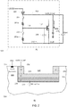
- FIG. 3A is a simplified schematic circuit diagram of a class D amplifier output stage 300 which comprises a regulated high side gate driver circuit in accordance with an example useful for understanding the invention.
- the skilled person will understand that the present regulated high side gate driver circuit in the alternative may be used to drive an output or power transistor of a single-phase or multiphase motor driver or a power transistor of a switched mode supply.
- the regulated high side gate driver structure is placed within the novel type of well-structure depicted on FIG. 3B ) which shows a simplified cross-sectional view of the novel well structure 324. As illustrated on FIG.
- the parasitic well capacitance 313 associated with the N-well diffusions 326, 330 is connected to the output terminal OUT of the class D amplifier output stage instead of to the high DC voltage terminal GVDD FLOAT as was the case in the prior art gate driver circuit illustrated on FIG. 2A ). For this reason the parasitic well capacitance 313 is coupled between the output terminal OUT, at node 312, and ground (GND) of the class D output stage in the present regulated high side gate driver circuit.
- the output terminal OUT is a low impedance node of the class D output stage which node is driven by the source terminal of the LDNMOS power transistor 307.
- the LDNMOS power transistor 307 When the LDNMOS power transistor 307 is placed in a conducting or on-state, it exhibits a low impedance and large current supply capability. Hence, the LDNMOS power transistor 307 can easily deliver the above-discussed parasitic well current INBL to charge and discharge the parasitic well capacitance 313. Consequently, undesired ripple voltage on the high DC voltage supply GVDD_FLOAT to the gate driver due to the previously discussed parasitic well current INBL has been eliminated. Therefore, the previously discussed external capacitor Cext that was required to reduce this voltage ripple on the high DC voltage of the prior art prior art regulated high side gate driver structure 100 has been eliminated.
- the high DC voltage supply GVDD FLOAT (node 306) to the gate driver is generated by a floating linear voltage regulator 305 in the present example of the gate driver as discussed in further detail below.
- the elimination of the external capacitor Cext leads to significant cost reduction and size reduction of the class D amplifier output stage and the corresponding class D audio amplifier solution.
- the skilled person will understand that other examples of the class D output stage may use a NMOS transistor, or PLDMOS transistor as the power transistor 307.
- the regulated high side gate driver circuit may comprise a CMOS inverter comprising a PMOS-NMOS transistor pair schematically depicted as pull-up and pull down resistances 301 a, 303a in series with respective ideal switches 301, 303.
- the regulated high side gate driver or circuit has a driver output 304 electrically coupled or connected to a gate terminal of a NMOS power transistor 307 on a high side of the class D output stage.
- the source terminal of the LDNMOS power transistor 307 is coupled to a load node or terminal OUT which is connectable to a loudspeaker load for sound reproduction.
- the drain terminal of the LDNMOS power transistor 307 may be coupled to a positive DC voltage supply or rail PVDD of the class D output stage or to a stacked power transistor.
- the class D output stage may further comprises a low side NMOS power transistor (not shown) as discussed in connection with the prior art class D output stage of FIG.
- the regulated high side gate driver circuit must be capable of driving a large capacitive load presented by the gate of the LDNMOS power transistor 307 as discussed above. Furthermore, the gate driver is capable of accurately driving the gate voltage of the LDNMOS power transistor 307 to a voltage level well-above the positive DC supply rail (not shown) of the class D output stage to accommodate the threshold voltage of the LDNMOS power transistor 307. This will ensure a low on-resistance of the LDMOS power transistor 307.
- the accurate setting of the gate voltage of the LDNMOS power transistor 307 is accomplished by supplying the regulated DC voltage GVDD_FLOAT to the gate driver 311 via the floating (relative to a ground node or ground potential, GND, of the class D output stage) linear voltage regulator 305.
- the linear voltage regulator is capable of generating a sufficiently high voltage level of the regulated DC voltage GVDD_FLOAT due to its connection to a high side DC voltage supply PVDD + GVDD of the class D amplifier.
- the high side DC voltage supply PVDD + GVDD is preferably a substantially fixed DC supply voltage which preferably is referred to the ground node or ground potential, GND of the class D output stage, i.e.
- the high side DC voltage supply is a ground referenced or non-floating DC voltage.
- the regulated DC voltage GVDD_FLOAT is referred to a voltage potential at a negative regulator input 312. This voltage potential is a high side negative supply voltage port of the floating linear voltage regulator 305.
- the floating linear voltage regulator 305 is schematically illustrated as comprising a linear regulating device in form of a LDMOS pass transistor 305 and a DC reference voltage generator VREF.
- the DC reference voltage generator VREF is connected between the negative regulator input 312 which also constitutes an audio output OUT of the class D output stage.
- the DC reference voltage generator VREF sets a predetermined DC reference voltage at a gate terminal, i.e. control terminal, of the LDMOS pass transistor 305 to set a suitable regulated and floating DC voltage GVDD_FLOAT at the regulator output node 306.
- a suitable smoothing or regulation capacitor Cr may be connected across VREF.
- the smoothing or regulation capacitor Cr may comprise a metal-insulator-metal (MIM) capacitor as discussed in further detail below.
- MIM metal-insulator-metal
- the floating linear voltage regulator 305 seeks to maintain a substantially constant DC voltage difference between the regulated DC voltage output GVDD_FLOAT and the negative regulator input 312.
- the level of the regulated DC voltage output GVDD_FLOAT with reference to the negative regulator input 312 may lie between 3 V and 6 V such as about 4.5 V for the same reasons as those discussed above in connection with the prior art embodiment of the high side gate driver circuit.
- the high side DC voltage supply PVDD + GVDD of the class D amplifier output stage forms the positive regulator input of the floating linear voltage regulator 305 and may for example possess a DC voltage level which is between 5 and 15 Volts higher than the positive DC supply rail of the class D output stage.
- the regulated DC voltage GVDD_FLOAT generated by the floating linear voltage regulator 305 is preferably supplied to the gate driver via the high side positive supply voltage port (not shown) of the gate driver.
- the skilled person will therefore appreciate that both the positive and negative regulator inputs of the floating linear voltage regulator 305 are floating relative to the ground GND potential of the class D output stage 300 as discussed above.
- a pulse width modulated audio signal may be supplied to a driver input (refer to item 414 of FIG. 4A )) of the gate driver via a suitable level shifter in a manner similar to the one illustrated on FIG. 1 .
- a level shifted replica of this pulse width modulated audio signal is supplied to the gate of the NMOS power transistor 307 via the driver output 304 of the gate driver.
- the movement of the parasitic well capacitance 313 of the regulated high side gate driver structure from the regulated DC supply voltage to the output terminal OUT of the class D output stage is explained below with reference to FIGS. 3B ), 4A) and 4B ).
- FIG. 3B shows a semiconductor layout of the novel well structure 324 before formation of the gate driver circuitry.
- the novel well structure 324 is formed in a P+ type epitaxial semiconductor substrate 322.
- the P + type epitaxial semiconductor substrate 322 is electrically connected to the ground (GND) potential of the class D output stage through a P+ diffusion contact 321 and suitable electrical wiring.
- the novel well structure 324 comprises a double junction isolation mechanism and structure with an extra P+ type buried layer 327 for the regulated high side gate driver structure.
- the novel well structure 324 comprises an N-well diffusion which comprises a horizontal N+ polarity buried layer (NBL) 326 and a vertical wall section 330 of N+ polarity semiconductor material.
- NBL horizontal N+ polarity buried layer
- the vertical wall section 330 is electrically coupled to the NBL 326 via an intermediate DNW layer 328 to form a complete N-well structure.
- the NBL 326 forms a bottom portion of the novel well-structure 324 which hence has a peripheral outer wall abutted to, or facing, the P type epitaxial semiconductor substrate 322.
- the N-well diffusion is electrically connected to the output terminal OUT 312 through an N+ diffusion contact 332 and suitable electrical wiring.
- a second well diffusion comprising P + polarity semiconductor material is arranged inside the N-well diffusion (326, 330, DNW) such that an outer peripheral wall of the second well diffusion is abutted to, or facing, an inner peripheral wall of the N-well diffusion.
- the second, or P-well, diffusion comprises a buried layer 327 which forms a horizontal bottom wall section of P-well diffusion.
- the P-well diffusion also comprises a vertical wall section 329 of P+ polarity semiconductor material which has a lowermost edge surface abutted and electrically connected to the horizontal bottom wall section 327.
- the P-well diffusion is electrically connected to the output terminal OUT 312 through a P+ diffusion contact 331 and suitable electrical wiring such that the P-well diffusion and the N-well diffusion are placed at the same electrical potential.
- the regulated high side gate driver circuit 417 comprises a gate driver 411 arranged inside or in the novel well structure 424.
- FIG. 4B shows a simplified cross-sectional view of the class D amplifier output stage 400 depicted on FIG. 4A ) except for LDNMOS power transistor 407 embedded in the P+ type epitaxial semiconductor substrate 422.
- the class D amplifier output stage 400 comprises an open-loop topology floating linear voltage regulator 417 comprising LDNMOS pass transistor 405.
- the LDNMOS pass transistor 405 is controlled by a DC reference voltage VREF connected to the gate terminal to set a suitable regulated DC voltage at node 406, GVDD_FLOAT, for the high side positive supply voltage port (source terminal of PMOS transistor 401) of the gate driver 411.
- the source terminal of the LDNMOS pass transistor 405 is provides the regulated DC voltage output GVDD_FLOAT while the drain terminal is connected to the positive regulator input which in turn is connected to the high side DC voltage supply PVDD + GVDD.
- This source follower configuration of the LDNMOS pass transistor 405 provides rapid transient response at the regulated DC voltage output.
- the rapid transient response is highly beneficial to provide good load regulation under demanding load conditions with extremely steep rising and falling PWM or PDM waveform edges at the low impedance output terminal OUT 412 at the source terminal of the LDNMOS power transistor 407.
- the high side DC voltage supply PVDD + GVDD is preferably a substantially fixed DC supply voltage which preferably is referred to the ground node or ground potential, GND of the class D output stage, i.e. the high side DC voltage supply is a ground referenced or non-floating DC voltage.
- the semiconductor layout of the LDMOS pass transistor 405 in the semiconductor substrate 422 is illustrated in cross-sectional view on the rightmost portion of FIG. 4B ).
- a source terminal of the LDNMOS pass transistor 405 is coupled to the high side positive supply voltage port of the gate driver 411 to provide an accurate and stable regulated DC voltage supply GVDD_FLOAT for the gate driver 411.
- One of the drain terminals of the pass transistor 405 of the floating voltage regulator is coupled to the high side DC voltage supply PVDD + GVDD of the class D audio amplifier.
- the novel well structure 424 which encloses, or houses, the gate driver 411 has a similar construction to the previously discussed well-structure 324 and corresponding features have been provided with corresponding reference numerals to ease comparison.
- the gate driver 411 of the regulated high side gate driver circuit 417 comprises a PMOS-NMOS transistor pair 401, 403 with a driver output 404 electrically coupled or connected to a gate terminal of the LDNMOS power transistor 407 arranged on a high side of the class D output stage. Drain, gate and source diffusions or terminals of the NMOS transistor 403 of the gate driver are arranged in a vertical wall section 429 of P+ polarity semiconductor material as illustrated on FIG. 4B . This vertical wall section 429 is a part of an inner P-well of the novel well structure 424.
- the novel well structure 424 additionally comprises an N+ polarity transistor body diffusion 435 arranged in abutment to the opposing wall segments of the vertical wall section 429 and above the horizontal P+ buried layer 427. Drain, gate and source diffusions or terminals of the PMOS transistor 401 of the gate driver 411 are arranged in the N+ polarity transistor body diffusion 435 as illustrated on FIG. 4B ). The gate terminals of the PMOS-NMOS transistor pair 401, 403 are electrically connected via a wire or trace 404 to form an input 414 of the gate driver.
- the PMOS source terminal and the NMOS drain terminal of transistor pair 401, 403 are electrically connected via a wire or trace 415 to form the output of the gate driver 411 which output is connected to the gate of power LDNMOS transistor 407 of the class D output stage.
- the electrical wire or trace 412 establishes an electrical connection between the source of the NMOS transistor 403, the inner P-well and the outer N-well of the novel well structure 424.
- the coupling of the parasitic well capacitance 413 (NBL-epi Cap) to the P type epitaxial semiconductor substrate 422 is schematically illustrated by the capacitor symbol413 on FIG.
- FIG 4A) and FIG 4B which illustrate how the parasitic well capacitance 413 has been eliminated at the regulated DC voltage output 406, GVDD_FLOAT, and instead connected to the low impedance output terminal OUT 412 of the class D output stage leading to the previously discussed benefits.
- FIG. 5 shows a schematic circuit diagram of a first embodiment of the regulated high side gate driver assembly or circuit 517.
- the present embodiment comprises an open loop topology floating voltage regulator 537 with a linear regulating device comprising a class AB output stage.
- the present class AB output stage has the advantageous capability of both sourcing current out of, and sinking current into, the regulated DC voltage output GVDD_FLOAT. This feature may lead to a more effective suppression of high-frequency ac ripple and/or noise on the regulated DC voltage output GVDD_FLOAT 506.
- the present regulated high side gate driver circuit 517 comprises the open-loop floating voltage regulator 537 coupled to a high side positive supply voltage port GVDD_FLOAT of an inverter configured gate driver 511.
- a high side negative supply voltage port 512 of the gate driver 511 is coupled to a negative regulator input of the floating voltage regulator 537 as illustrated.
- This negative regulator input is also coupled to the Class AB output stage and a DC voltage reference generator 30 of the floating voltage regulator 537.
- the DC reference voltage generator comprises a Zener diode 534 and a first constant current source IDC1 connected between the cathode of the Zener diode and the high side DC voltage supply PVDD + GVDD via a reverse voltage protection diode 536.
- the high side DC voltage supply PVDD + GVDD is preferably a substantially fixed DC supply voltage which preferably is referred to the ground node or ground potential of a circuit into which the regulated high side gate driver circuit 517 is integrated such as a class D audio amplifier output stage.
- the Zener diode 534 is connected to the negative regulator input 512.
- the first constant current source IDC1 supplies a predetermined bias current in the reverse direction of the Zener diode 534 such that reasonable stable Zener knee voltage is developed across the Zener diode 534 and the Zener voltage is used as a DC reference voltage VREF for the floating regulator.
- the DC reference voltage VREF is applied to an input terminal 508a of the class AB output stage.
- the class AB output stage comprises a first output transistor 505a connected between the positive regulator input (at node PVDD+ GVDD) and the regulated DC voltage output 506 and a second output transistor 505b connected between the regulated DC voltage output 506 and the negative regulator input 512.
- the cascade connection of diode connected MOS transistors 530, 532 and a second constant current source IDC2 forms a DC bias voltage circuit for the first and second output transistors 505a, 505b to set a suitable DC bias current therein.
- the DC bias voltage circuit is connected between respective gage or control terminals of the first and second output transistors 505a, 505b.
- the regulated DC output voltage at the regulated DC voltage output 506 will be approximately one gate-source voltage drop V GS of the first transistor 505a lower than the DC reference voltage VREF.
- the floating voltage regulator 537 preferably comprises a smoothing or regulation capacitor Cr which is connected across VREF.
- the regulation capacitor Cr comprises a metal-insulator-metal (MIM) capacitor which is arranged above the residual passive and active semiconductor components of the high side gate driver circuit 517 on the semiconductor substrate. Since the capacitance, and thereby dimensions, of the regulation capacitor Cr should be relatively large to provide optimal ripple suppression, it is important to minimize die area consumption by Cr. This may advantageously be achieved by placing Cr in a set of layers of the semiconductor substrate arranged on top of another set layers which holds the residual active and passive integrated circuit components of the regulated high side gate driver circuit 517.
- the metal-insulator-metal (MIM) capacitor may for example partly or fully cover the residual active and passive integrated circuit components of the regulated high side gate driver circuit 517.
- the capacitance of Cr may lie between 1 pF and 100 pF.
- the role of the regulation capacitor Cr in the floating voltage regulator 537 comprises suppressing noise and ripple on the DC reference voltage generator and acting as a fast responding current/energy reservoir for the class AB output stage allowing the regulated DC voltage output 506 to provide adequate supply current to the gate driver 511.
- the fast response of the regulated DC voltage output 506 is important to adequately suppress high frequency ripple or spike voltages thereon imparted by the previously discussed fast transient current pulses drawn by the gate driver 511 during operation of the class D audio amplifier.
- the input signal at the input IN of the gate driver 511 may comprise a pulse width modulated (PWM) or pulse density modulated (PDM) audio signal with extremely fast rising and falling waveform edges such as rise and fall times around 1 ns.
- PWM pulse width modulated
- PDM pulse density modulated
- FIG. 6 shows a schematic circuit diagram of a second embodiment of a regulated high side gate driver circuit 617.
- the skilled person will understand that the present regulated high side gate driver circuit 617 may be arranged in the previously discussed novel well structure of the semiconductor substrate or arranged in a standard LDMOS semiconductor substrate.
- the present high side gate driver circuit 617 comprises a floating voltage regulator 637 based on a shunt regulation circuit 634.
- the skilled person will understand that the shunt regulation circuit 634 may largely replace the Zener diode 534 of the second embodiment as a voltage reference generating element.
- class AB output stage comprising first and second output transistors 605a, 605b, and the DC bias voltage circuit, comprising IDC2 and transistors 630, 632, may have the same functionality and electrical characteristics as those of the corresponding circuit components of the first embodiment of the high side gate driver circuit 517.
- the shunt regulation circuit 634 comprises a shunt transistor 635 and the regulated DC voltage is controlled by a variable current sinking through the shunt transistor 635.
- the floating voltage regulator 637 comprises a linear pass transistor 605 acting as a regulating device which is connected between the high side DC voltage supply PVDD + GVDD and the regulated DC voltage output GVDD_FLOAT 606.
- the linear pass transistor 605 is controlled by an output VREF1 of the shunt regulation circuit 634 connected to a gate terminal of the linear pass transistor.
- the shunt regulation circuit 634 further comprises an error amplifier 623 having an output coupled to the gate or control terminal of the shunt transistor 635.
- a first input of the error amplifier 623 is connected to a voltage divider comprising resistors R1 r and Rr2. A first end of the voltage divider is connected to VREF1 while the second end is connected to the negative regulator input at node 612 of the shunt voltage regulator 637. A tapping point or node 621 in-between Rs1 and Rs2 provides a shunt voltage to the first input of the error amplifier 623 proportional to the VREF1 voltage.
- the second input of the error amplifier 623 is connected to a DC reference voltage VREF2 which may be generated by, or derived from, a suitable temperature stable voltage reference such as a bandgap voltage reference.
- the error amplifier 623 reacts to changes of the regulated DC voltage by either increasing or decreasing the control or gate voltage of the shunt transistor 635 to counteract the change of the VREF1 voltage and thereby seeking to maintain or stabilize the to the regulated DC voltage output GVDD_FLOAT at a desired or target DC voltage.
- the shunt regulation circuit 634 comprises a feedback loop from VREF1 voltage back to the gate of the shunt transistor 635.
- the regulated DC voltage is sensed through the voltage divider and the error amplifier 623.
- the feedback loop configuration does not introduce any noticeable time delay in the response of the shunt regulator circuit since the loop only extends from the drain terminal to the gate terminal of the shunt transistor 635.
- the error amplifier 623 may comprise a differential amplifier for example an operational amplifier where the first input of the error amplifier 623 is a non-inverting input of the operational amplifier and the second input is an inverting input of the operational amplifier, or vice versa.
- the shunt transistor 635 may comprise various types of transistors such as a BJT or MOSFET.
- the shunt transistor 635 comprises a drain extended NMOS (DE-NMOS) transistor.
- the DE-NMOS transistor comprises a first drain terminal connected to the VREF1 voltage and a second or extended drain terminal connected to the regulated DC voltage output GVDD_FLOAT.
- the present high side gate driver circuit 617 does not comprise the previously discussed Zener diode 534 of the first embodiment of the invention to set the DC reference voltage VREF1.
- the omission of the Zener diode is advantageous because this feature avoids that the negative buried layer (NBL) of the cathode of the Zener diode is brought in contact with the semiconductor substrate and thereby opens a potential noise injection path to the DC reference voltage VREF1.
- the negative buried layer (NBL) of the cathode of the Zener diode forms an undesired parasitic capacitance to the semiconductor substrate.
- the role and properties of the regulation capacitor Cr may the same as the previously discussed properties in connection with the description of the regulation capacitor Cr of the first embodiment of the regulated high side gate driver circuit 517.
- FIG. 7 shows a schematic circuit diagram of a class D amplifier circuit 701 which comprises a multi-level class D audio amplifier output stage 703 driven by respective regulated high side gate driver circuits 517a, 517b, 517c, 517d.
- Each of the regulated high side gate driver circuits 517a, 517b, 517c, and 517d may comprise a regulated high side gate driver circuit in accordance with one of the previously discussed embodiments thereof.
- the multi-level class D audio amplifier output stage or output stage 703 comprises a four stacked power transistors SW1, SW2, SW3, SW4 connected in cascade between a positive power supply rail PVDD and a negative power supply rail, in form of ground potential GND in the present embodiment, of the class D amplifier circuit 701.
- the gate terminals of the four stacked power transistors SW1, SW2, SW3, SW4 are connected to respective floating and regulated DC voltage outputs 504a, 504b, 504c, 504d of the high side gate driver circuits 517a, 517b, 517c, 517d such that each power transistor is switched between conducting and non-conducting states in accordance with the gate voltage of the power transistor in question.
- a source terminal of each of the four stacked power transistors SW1, SW2, SW3, and SW4 is connected to the negative regulator input of the particular regulated high side gate driver circuit driving the gate terminal of the same power transistor.
- the multi-level class D audio amplifier output stage 703 comprises a first leg which comprises the first and second cascaded power transistors SW1, SW2 connected between the positive power supply rail PVDD and a signal output VOUT of the output stage.
- the multi-level class D audio amplifier output stage 703 further comprises a second leg which comprises the third and fourth cascaded power transistors SW3, SW4 connected in cascade between the signal output Vout and the negative power supply rail GND.
- a flying capacitor Cfly is connected between a first intermediate output stage node 705 arranged between the first and second cascaded power transistors and a second intermediate output stage node 707 arranged between the third and fourth cascaded power transistors.
- the flying capacitor is preferably charged to one-half of the voltage difference between the positive and negative power supply rails PVDD and GND to set a mid-point voltage at the signal output Vout.
Landscapes
- Engineering & Computer Science (AREA)
- Power Engineering (AREA)
- Amplifiers (AREA)
Claims (13)
- Regulierte, hochseitige Gate-Ansteuereinrichtungsschaltung (517) für Leistungstransistoren, die Folgendes umfasst:eine Gate-Ansteuereinrichtung (511), die einen hochseitigen positiven Versorgungsspannungsanschluss (506), einen hochseitigen negativen Versorgungsspannungsanschluss (512), einen Ansteuereinrichtungseingang (IN) und einen Ansteuereinrichtungsausgang (504) umfasst; undeinen Schwebespannungsregulator, der Folgendes umfasst:einen positiven Regulatoreingang, der mit einer hochseitigen Gleichstrom-Spannungsversorgung (PVDD+GVDD) verbunden werden kann,einen regulierten Gleichstrom-Spannungsausgang (GVDD_FLOAT),einen negativen Regulatoreingang,eine lineare Regulierungsvorrichtung, die mit dem regulierten Gleichstrom-Spannungsausgang (GVDD_FLOAT) verbunden ist und zum Unterdrücken von Rauschen und einer Brummspannung auf der hochseitigen Gleichstrom-Spannungsversorgung (PVDD+GVDD) im regulierten Gleichstrom-Spannungsausgang (GVDD-FLOAT) konfiguriert ist,einen Gleichstrom-Referenzspannungsgenerator, der konfiguriert ist, an einem Steueranschluss der linearen Regulierungsvorrichtung eine Gleichstrom-Referenzspannung (VREF) zu erzeugen, um einen Gleichstrom-Spannungspegel am regulierten Gleichstrom-Spannungsausgang (GVDD_FLOAT) einzustellen,einen Regulierungskondensator (Cr), der zwischen dem positiven und dem negativen Anschluss des Gleichstrom-Referenzspannungsgenerators verbunden ist;wobei der negative Regulatoreingang mit dem hochseitigen negativen Versorgungsspannungsanschluss (512) verbunden ist und der regulierte Gleichstrom-Spannungsausgang (GVDD_FLOAT) mit dem hochseitigen positiven Versorgungsspannungsanschluss der Gate-Ansteuereinrichtung (511) verbunden ist;wobei die lineare Regulierungsvorrichtung eine Ausgangsstufe der Klasse AB umfasst, die einen positiven Stromversorgungsanschluss, der mit dem positiven Regulatoreingang verbunden ist, und einen negativen Stromversorgungsanschluss, der mit dem negativen Regulatoreingang verbunden ist, aufweist; undwobei ein Steueranschluss (508a, 508b) der Ausgangsstufe der Klasse AB mit der Gleichstrom-Referenzspannung (VREF) verbunden ist und ein Ausgang (506) der Ausgangsstufe der Klasse AB mit dem regulierten Gleichstrom-Spannungsausgang (GVDD_FLOAT) verbunden ist, um in eine Last am regulierten Gleichstrom-Spannungsausgang Strom einzuspeisen oder davon Strom abzuziehen;wobei die Ausgangsstufe der Klasse AB Folgendes umfasst:einen ersten Ausgangstransistor (505a), der zwischen dem positiven Regulatoreingang und dem regulierten Gleichstrom-Spannungsausgang (GVDD_FLOAT) verbunden ist,einen zweiten Ausgangstransistor (505b), der zwischen dem negativen Regulatoreingang (512) und dem regulierten Gleichstrom-Spannungsausgang (GVDD_FLOAT) verbunden ist; undeine Vorspannungsschaltung, die zwischen den jeweiligen Steueranschlüssen (508a, 508b) des ersten und des zweiten Ausgangstransistors (505a, 505b) verbunden ist, um darin einen vorgegebenen Gleichstrom-Vorstrom einzustellen.
- Regulierte, hochseitige Gate-Ansteuereinrichtungsschaltung (517) nach Anspruch 1, wobei der Regulierungskondensator (Cr) einen Metall-Isolator-Metall-Kondensator (MIM-Kondensator) umfasst.
- Regulierte, hochseitige Gate-Ansteuereinrichtungsschaltung (517) nach Anspruch 2, wobei der Metall-Isolator-Metall-Kondensator (MIM-Kondensator) eine Kapazität zwischen 1 pF und 100 pF wie etwa zwischen 10 pF und 50 pF aufweist.
- Regulierte, hochseitige Gate-Ansteuereinrichtungsschaltung (517) nach einem der vorhergehenden Ansprüche wobei der Schwebespannungsregulator eine Topologie mit offener Schleife ohne eine Spannungs- oder Stromregulierungsrückkopplungsschleife vom regulierten Gleichstrom-Spannungsausgang (GVDD_FLOAT) zurück zum Steueranschluss der linearen Regulierungsvorrichtung (505a, 505b) umfasst.
- Regulierte, hochseitige Gate-Ansteuereinrichtungsschaltung (517) nach einem der vorhergehenden Ansprüche, wobei die lineare Regulierungsvorrichtung Folgendes umfasst:
einen Durchgangstransistor (505a), der zwischen dem positiven Regulatoreingang und dem regulierten Gleichstrom-Spannungsausgang (GVDD_FLOAT) verbunden ist, wobei ein Steueranschluss des Durchgangstransistors (505a) mit der Gleichstrom-Referenzspannung (VREF) verbunden ist, die durch den Gleichstrom-Referenzspannungsgenerator erzeugt wird. - Regulierte, hochseitige Gate-Ansteuereinrichtungsschaltung (517) nach Anspruch 5, wobei der Durchgangstransistor (505a) einen MOSFET oder einen bipolaren Transistor umfasst, wobei eine Source oder ein Emitter jeweils mit dem regulierten Gleichstrom-Spannungsausgang verbunden ist, und ein Drain oder ein Kollektoranschluss jeweils mit dem positiven Regulatoreingang verbunden ist.
- Regulierte, hochseitige Gate-Ansteuereinrichtungsschaltung (517) nach einem der vorhergehenden Ansprüche, wobei der Gleichstrom-Referenzspannungsgenerator eine umgekehrt vorgespannte Zener-Diode (534) umfasst.
- Regulierte, hochseitige Gate-Ansteuereinrichtungsschaltung (517) nach einem der Ansprüche 1-7, wobei der Gleichstrom-Referenzspannungsgenerator eine Shunt-Regulatorschaltung umfasst.
- Regulierte, hochseitige Gate-Ansteuereinrichtungsschaltung (517) nach Anspruch 8, wobei die Shunt-Regulatorschaltung Folgendes umfasst:einen Shunt-Transistor, der zwischen der Gleichstrom-Referenzspannung und dem negativen Regulatoreingang verbunden ist,einen Fehlerverstärker, der einen Ausgang, einen ersten Eingang und einen zweiten Eingang umfasst, wobei der Ausgang mit einem Steueranschluss des Shunt-Transistors verbunden ist,einen Spannungsteiler, der mit der Gleichstrom-Referenzspannung verbunden ist und konfiguriert ist, dem ersten Eingang des Fehlerverstärkers eine Shunt-Spannung zuzuführen, die zur Gleichstrom-Referenzspannung proportional ist,eine zweite Gleichstrom-Spannungsreferenz, die mit dem zweiten Eingang des Fehlerverstärkers verbunden ist.
- Regulierte, hochseitige Gate-Ansteuereinrichtungsschaltung (517) nach einem der vorhergehenden Ansprüche, die Folgendes umfasst:ein Halbleitersubstrat (P-EPI), das ein Halbleitermaterial mit einer ersten Polarität umfasst, in dem eine erste Wannendiffusion (326, 330) gebildet ist,wobei die erste Wannendiffusion (326, 330) ein Halbleitermaterial mit einer zweiten Polarität umfasst und eine umlaufende Außenwand aufweist, die am Halbleitersubstrat (P-EPI) anliegt,eine zweite Wannendiffusion (329), die ein Halbleitermaterial mit der ersten Polarität umfasst, die im Inneren der ersten Wannendiffusion (326, 330) angeordnet ist, derart, dass eine Außenumfangswand der zweiten Wannendiffusion (329) an einer Innenumfangswand der ersten Wannendiffusion (326, 330) anliegt; unddie Gate-Ansteuereinrichtung, die in der zweiten Wannendiffusion (329) angeordnet ist;eine elektrische Verbindung jeweils zwischen der ersten und der zweiten Wannendiffusion und dem hochseitigen negativen Versorgungsspannungsanschluss (312) der Gate-Ansteuereinrichtung.
- Integriertes Halbleitersubstrat, das Folgendes umfasst:eine regulierte, hochseitige Gate-Ansteuereinrichtungsschaltung (517) nach einem der Ansprüche 2-10, wobei die Komponenten der integrierten Schaltung der Gate-Ansteuereinrichtung und die Komponenten der integrierten Schaltung des Schwebespannungsregulators mit Ausnahme des Regulierungskondensators in einer ersten Gruppe von Schichten des Halbleitersubstrats integriert sind, undder Metall-Isolator-Metall-Kondensator (MIM-Kondensator) in einer zweiten Gruppe von Schichten des Halbleitersubstrats integriert ist, die über der ersten Gruppe von Schichten angeordnet ist, derart, dass der Metall-Isolator-Metall-Kondensator (MIM-Kondensator) die Komponenten der integrierten Schaltung der Gate-Ansteuereinrichtung und des Schwebespannungsregulators zumindest teilweise überlagert.
- Audioverstärkerausgangsstufe (703) der Klasse D, die Folgendes umfasst:mehrere gestapelte Leistungstransistoren (SW1, SW2, SW3, SW4), die zwischen einer positiven Stromversorgungsschiene (PVDD) und einer negativen Stromversorgungsschiene (GND) des Audioverstärkers (701) der Klasse D verbunden sind,wobei die mehreren gestapelten Leistungstransistoren (SW1, SW2, SW3, SW4) jeweilige Steueranschlüsse (504a, 504b, 504c, 504d) umfassen, die konfiguriert sind, jeden Leistungstransistor in Übereinstimmung mit einer Steuerspannung zwischen einem leitenden Zustand und einem nicht leitenden Zustand umzuschalten,mehrere regulierte, hochseitige Gate-Ansteuereinrichtungsschaltungen (GD1, GD2, GD3, GD4) nach einem der Ansprüche 1-10, wobei die Ansteuereinrichtungsausgänge der mehreren spannungsregulierten, hochseitigen Gate-Ansteuereinrichtungsschaltungen mit den jeweiligen Steueranschlüssen (504a, 504b, 504c, 504d) der mehreren gestapelten Leistungstransistoren (SW1, SW2, SW3, Sw4) verbunden sind; undwobei die Source-Anschlüsse der mehreren gestapelten Leistungstransistoren mit den jeweiligen der hochseitigen negativen Versorgungsspannungsanschlüsse der mehreren regulierten, hochseitigen Gate-Ansteuereinrichtungsschaltungen verbunden sind.
- Audioverstärkerausgangsstufe (703) der Klasse D nach Anspruch 12, wobei die mehreren gestapelten Leistungstransistoren (SW1, SW2, SW3, Sw4) Folgendes umfassen:einen ersten Zweig, der mindestens einen ersten und einen zweiten Kaskaden-Leistungstransistor, die zwischen der positiven Stromversorgungsschiene (PVDD) und einem Signalausgang (Vout) der Ausgangsstufe verbunden sind, umfasst, undeinen zweiten Zweig, der mindestens einen dritten und einen vierten Kaskaden-Leistungstransistor, die zwischen dem Signalausgang (Vout) und einer negativen Stromversorgungsschiene (GND) der Ausgangsstufe verbunden sind, umfasst.
Applications Claiming Priority (2)
| Application Number | Priority Date | Filing Date | Title |
|---|---|---|---|
| EP14197057 | 2014-12-09 | ||
| PCT/EP2015/077677 WO2016091593A1 (en) | 2014-12-09 | 2015-11-25 | A regulated high side gate driver circuit for power transistors |
Publications (2)
| Publication Number | Publication Date |
|---|---|
| EP3231090A1 EP3231090A1 (de) | 2017-10-18 |
| EP3231090B1 true EP3231090B1 (de) | 2019-04-24 |
Family
ID=52013954
Family Applications (1)
| Application Number | Title | Priority Date | Filing Date |
|---|---|---|---|
| EP15802043.8A Active EP3231090B1 (de) | 2014-12-09 | 2015-11-25 | Geregelte spannungsseitige gatetreiberschaltung für leistungstransistoren |
Country Status (6)
| Country | Link |
|---|---|
| US (2) | US10504769B2 (de) |
| EP (1) | EP3231090B1 (de) |
| JP (1) | JP6728173B2 (de) |
| KR (1) | KR102492494B1 (de) |
| CN (1) | CN107005144B (de) |
| WO (1) | WO2016091593A1 (de) |
Families Citing this family (36)
| Publication number | Priority date | Publication date | Assignee | Title |
|---|---|---|---|---|
| KR102492494B1 (ko) * | 2014-12-09 | 2023-01-30 | 인피니언 테크놀로지스 오스트리아 아게 | 전력 트랜지스터들을 위한 조절된 하이 사이드 게이트 드라이버 회로 |
| KR20170076497A (ko) * | 2015-12-24 | 2017-07-04 | 삼성전기주식회사 | 드라이브 회로 |
| FR3059490B1 (fr) * | 2016-11-25 | 2018-11-16 | Exagan | Dispositif de commutation d'un circuit de puissance presentant un circuit passif de protection |
| US10193444B1 (en) * | 2017-07-28 | 2019-01-29 | Pixart Imaging Inc. | Reference voltage generator with adaptive voltage and integrated circuit chip |
| US10778213B2 (en) * | 2017-10-05 | 2020-09-15 | Rohm Co., Ltd. | Driving circuit for output transistor |
| US10581312B2 (en) * | 2017-12-29 | 2020-03-03 | Texas Instruments Incorporated | Multilevel converter using node voltage track and control |
| US10404175B2 (en) | 2017-12-29 | 2019-09-03 | Texas Instruments Incorporated | Converter topology with adaptive power path architecture |
| IT201800001660A1 (it) * | 2018-01-23 | 2019-07-23 | St Microelectronics Grenoble 2 | Circuito di pilotaggio, sistema e procedimento corrispondenti |
| US10153795B1 (en) * | 2018-02-20 | 2018-12-11 | Nxp B.V. | Switching amplifier circuit with amplitude control |
| US10804691B2 (en) * | 2018-03-06 | 2020-10-13 | Texas Instruments Incorporated | Circuit providing reverse current protection for high-side driver |
| JP7043139B2 (ja) * | 2018-06-25 | 2022-03-29 | エイブリック株式会社 | 逆流防止回路及び電源回路 |
| US11201613B2 (en) | 2018-07-31 | 2021-12-14 | Taiwan Semiconductor Manufacturing Company, Ltd. | Driver circuit and method of operating the same |
| TWI723470B (zh) | 2018-07-31 | 2021-04-01 | 台灣積體電路製造股份有限公司 | 驅動電路、積體電路、及操作驅動電路的方法 |
| US10826485B2 (en) * | 2018-12-17 | 2020-11-03 | Analog Devices International Unlimited Company | Cascode compound switch slew rate control |
| US10795392B1 (en) * | 2019-04-16 | 2020-10-06 | Novatek Microelectronics Corp. | Output stage circuit and related voltage regulator |
| EP3736982A1 (de) * | 2019-05-07 | 2020-11-11 | Siemens Aktiengesellschaft | Adaptive schaltgeschwindigkeitssteuerung von leistungshalbleitern |
| CN112532027B (zh) * | 2019-09-18 | 2021-12-03 | 圣邦微电子(北京)股份有限公司 | 一种多级功率管驱动电路 |
| US11469669B2 (en) * | 2020-01-31 | 2022-10-11 | Texas Instruments Incorporated | Methods and circuitry to detect PFM mode entry in wide duty range DC converter |
| US11196396B2 (en) * | 2020-02-12 | 2021-12-07 | Himax Technologies Limited | Operational amplifier |
| CN111211764B (zh) * | 2020-02-18 | 2023-10-24 | 恩智浦有限公司 | 栅极电压控制 |
| CN111404411B (zh) * | 2020-02-26 | 2021-06-15 | 北京交通大学 | 一种抑制串扰的三电平有源驱动电路 |
| CN111541430B (zh) * | 2020-05-21 | 2023-05-12 | 张金路 | 一种复合型串联数字功放 |
| CN111796623B (zh) * | 2020-08-19 | 2021-09-14 | 北京新雷能科技股份有限公司 | 一种高压供电的ptat基准电流源电路 |
| US11606029B2 (en) * | 2020-09-10 | 2023-03-14 | Stmicroelectronics International N.V. | DC-DC voltage converter with floating rail generation for cascode transistor biasing |
| EP4033661B1 (de) | 2020-11-25 | 2024-01-24 | Changxin Memory Technologies, Inc. | Steuerschaltung und verzögerungsschaltung |
| EP4033312B1 (de) | 2020-11-25 | 2024-08-21 | Changxin Memory Technologies, Inc. | Steuerschaltung und verzögerungsschaltung |
| US11681313B2 (en) | 2020-11-25 | 2023-06-20 | Changxin Memory Technologies, Inc. | Voltage generating circuit, inverter, delay circuit, and logic gate circuit |
| EP4033664B1 (de) * | 2020-11-25 | 2024-01-10 | Changxin Memory Technologies, Inc. | Potentialerzeugungsschaltung, inverter, verzögerungsschaltung und logische gatterschaltung |
| CN114696573B (zh) * | 2020-12-30 | 2025-08-08 | 华润微集成电路(无锡)有限公司 | 自举电路中实现提高功率mos管栅压的栅极驱动电路结构 |
| DE102021107464A1 (de) | 2021-03-25 | 2022-09-29 | Rheinisch-Westfälische Technische Hochschule (Rwth) Aachen | Isolierte Gate-Treiberschaltung und Verfahren zum Betreiben der isolierten Gate-Treiberschaltung |
| US11757393B2 (en) * | 2021-10-19 | 2023-09-12 | Dana Tm4 Inc. | Integrated power module with transformer-less gate driver for high voltage power inverters |
| CN115021539B (zh) * | 2022-08-09 | 2022-11-04 | 无锡力芯微电子股份有限公司 | 一种防电流反灌的电路结构 |
| CN115333518B (zh) * | 2022-10-14 | 2023-01-03 | 高澈科技(上海)有限公司 | 高压模拟集成开关电路 |
| IT202300004365A1 (it) * | 2023-03-09 | 2024-09-09 | St Microelectronics Int Nv | Circuito di pilotaggio con controllo di scarica, sistema elettronico e veicolo corrispondenti |
| CN117348668B (zh) * | 2023-11-06 | 2026-03-31 | 安徽皖仪科技股份有限公司 | 一种高精度双极线性高压调节电路 |
| KR20260009159A (ko) | 2024-07-10 | 2026-01-19 | 주식회사 실리콘마이터스 | 전력 전달 조절 기능이 구비된 스위치드 커패시터 컨버터 |
Family Cites Families (18)
| Publication number | Priority date | Publication date | Assignee | Title |
|---|---|---|---|---|
| JPH11225470A (ja) * | 1998-02-04 | 1999-08-17 | Hitachi Ltd | スイッチング素子ドライブ用電源回路 |
| JP3941549B2 (ja) * | 2002-03-06 | 2007-07-04 | ヤマハ株式会社 | D級増幅器 |
| US6727758B2 (en) * | 2002-05-28 | 2004-04-27 | Koninklijke Philips Electronics N.V. | Fast cascaded class AB bipolar output stage |
| US6836173B1 (en) * | 2003-09-24 | 2004-12-28 | System General Corp. | High-side transistor driver for power converters |
| EP1580872B1 (de) * | 2004-03-26 | 2016-05-11 | DET International Holding Limited | Steuerschaltung |
| US7564225B2 (en) * | 2005-09-28 | 2009-07-21 | Monolithic Power Systems, Inc. | Low-power voltage reference |
| US8427235B2 (en) * | 2007-04-13 | 2013-04-23 | Advanced Analogic Technologies, Inc. | Power-MOSFETs with improved efficiency for multi-channel class-D audio amplifiers and packaging thereof |
| JP2010226334A (ja) * | 2009-03-23 | 2010-10-07 | Sanyo Electric Co Ltd | パルス幅変調増幅器 |
| JP5545045B2 (ja) * | 2010-06-04 | 2014-07-09 | 富士電機株式会社 | コンパレータ回路 |
| JP2012019625A (ja) * | 2010-07-08 | 2012-01-26 | Ricoh Co Ltd | 駆動回路、該駆動回路を備えた半導体装置、これらを用いたスイッチングレギュレータおよび電子機器 |
| TW201218631A (en) * | 2010-10-19 | 2012-05-01 | Analog Integrations Corp | Bootstrap circuit without a regulator and a diode |
| US8283979B2 (en) * | 2011-01-19 | 2012-10-09 | Harman International Industries, Incorporated | Amplifier system for a power converter |
| JP6480184B2 (ja) * | 2011-06-14 | 2019-03-06 | インフィネオン テクノロジーズ オーストリア アクチエンゲゼルシャフト | パワートランジスタのゲートドライバ |
| JP6486385B2 (ja) * | 2014-01-21 | 2019-03-20 | インフィネオン テクノロジーズ オーストリア アクチエンゲゼルシャフト | 集積化ハイサイド・ゲート・ドライバー構造、及びハイサイド・パワー・トランジスターを駆動する回路 |
| KR102492494B1 (ko) * | 2014-12-09 | 2023-01-30 | 인피니언 테크놀로지스 오스트리아 아게 | 전력 트랜지스터들을 위한 조절된 하이 사이드 게이트 드라이버 회로 |
| JP6328075B2 (ja) * | 2015-04-30 | 2018-05-23 | ローム株式会社 | 比較回路、電源制御ic、スイッチング電源装置 |
| US9712058B1 (en) * | 2016-08-29 | 2017-07-18 | Silanna Asia Pte Ltd | High speed tri-level input power converter gate driver |
| US10447160B2 (en) * | 2017-05-16 | 2019-10-15 | Semiconductor Components Industries, Llc | Pulse width control for switching mode power converters |
-
2015
- 2015-11-25 KR KR1020177017723A patent/KR102492494B1/ko active Active
- 2015-11-25 US US15/532,025 patent/US10504769B2/en active Active
- 2015-11-25 JP JP2017530318A patent/JP6728173B2/ja active Active
- 2015-11-25 CN CN201580066987.XA patent/CN107005144B/zh active Active
- 2015-11-25 WO PCT/EP2015/077677 patent/WO2016091593A1/en not_active Ceased
- 2015-11-25 EP EP15802043.8A patent/EP3231090B1/de active Active
-
2019
- 2019-11-01 US US16/672,038 patent/US10854500B2/en active Active
Non-Patent Citations (1)
| Title |
|---|
| None * |
Also Published As
| Publication number | Publication date |
|---|---|
| KR20170092605A (ko) | 2017-08-11 |
| US10504769B2 (en) | 2019-12-10 |
| US20170271195A1 (en) | 2017-09-21 |
| WO2016091593A1 (en) | 2016-06-16 |
| JP6728173B2 (ja) | 2020-07-22 |
| CN107005144A (zh) | 2017-08-01 |
| CN107005144B (zh) | 2020-01-31 |
| US10854500B2 (en) | 2020-12-01 |
| JP2017537551A (ja) | 2017-12-14 |
| EP3231090A1 (de) | 2017-10-18 |
| US20200135536A1 (en) | 2020-04-30 |
| KR102492494B1 (ko) | 2023-01-30 |
Similar Documents
| Publication | Publication Date | Title |
|---|---|---|
| US10854500B2 (en) | Gate driver circuitry for power transistors | |
| US10096705B2 (en) | Integrated high side gate driver structure and circuit for driving high side power transistors | |
| US11658654B2 (en) | DC-coupled high-voltage level shifter | |
| US10348293B2 (en) | Timing controller for dead-time control | |
| EP2517343B1 (de) | Dc/dc-umwandlung mit gestapelten nmos transistoren | |
| EP2517342B1 (de) | Überspannungsschutz für einen schaltumrichter | |
| US9912327B2 (en) | Dead time control circuit for a level shifter | |
| US9035625B2 (en) | Common cascode routing bus for high-efficiency DC-to-DC conversion | |
| US11133797B1 (en) | Bootstrap circuit for gate driver | |
| TW201304411A (zh) | 半導體裝置、使用其之換流器、轉換器及電力轉換裝置 | |
| US8854089B2 (en) | Power switch driving circuits and power converters thereof | |
| KR20170131452A (ko) | 파워 fet들의 캐스코드 스택용 드라이브 | |
| US20250088104A1 (en) | Driver for slew-rate control of phase node in buck converter | |
| WO2015175012A1 (en) | Method and circuitry for sensing and controlling a current | |
| JP4311683B2 (ja) | 半導体装置、降圧チョッパレギュレータ、電子機器 | |
| US20240022163A1 (en) | Driving circuit, semiconductor device including the same, and switching power supply device including the same | |
| Wicht | Tutorial: Analog Building Blocks of DC-DC Converters | |
| US20160315590A1 (en) | Audio amplifier circuit, audio output device using the same, and electronic device using the same |
Legal Events
| Date | Code | Title | Description |
|---|---|---|---|
| STAA | Information on the status of an ep patent application or granted ep patent |
Free format text: STATUS: THE INTERNATIONAL PUBLICATION HAS BEEN MADE |
|
| PUAI | Public reference made under article 153(3) epc to a published international application that has entered the european phase |
Free format text: ORIGINAL CODE: 0009012 |
|
| STAA | Information on the status of an ep patent application or granted ep patent |
Free format text: STATUS: REQUEST FOR EXAMINATION WAS MADE |
|
| 17P | Request for examination filed |
Effective date: 20170602 |
|
| AK | Designated contracting states |
Kind code of ref document: A1 Designated state(s): AL AT BE BG CH CY CZ DE DK EE ES FI FR GB GR HR HU IE IS IT LI LT LU LV MC MK MT NL NO PL PT RO RS SE SI SK SM TR |
|
| AX | Request for extension of the european patent |
Extension state: BA ME |
|
| DAV | Request for validation of the european patent (deleted) | ||
| DAX | Request for extension of the european patent (deleted) | ||
| STAA | Information on the status of an ep patent application or granted ep patent |
Free format text: STATUS: EXAMINATION IS IN PROGRESS |
|
| RAP1 | Party data changed (applicant data changed or rights of an application transferred) |
Owner name: INFINEON TECHNOLOGIES AUSTRIA AG |
|
| 17Q | First examination report despatched |
Effective date: 20180808 |
|
| GRAP | Despatch of communication of intention to grant a patent |
Free format text: ORIGINAL CODE: EPIDOSNIGR1 |
|
| STAA | Information on the status of an ep patent application or granted ep patent |
Free format text: STATUS: GRANT OF PATENT IS INTENDED |
|
| RIC1 | Information provided on ipc code assigned before grant |
Ipc: H01L 21/8238 20060101ALI20181024BHEP Ipc: H01L 27/092 20060101ALI20181024BHEP Ipc: H03K 17/06 20060101AFI20181024BHEP Ipc: H03K 17/687 20060101ALI20181024BHEP Ipc: H03F 3/217 20060101ALI20181024BHEP Ipc: H02M 1/08 20060101ALI20181024BHEP Ipc: H01L 21/761 20060101ALI20181024BHEP |
|
| INTG | Intention to grant announced |
Effective date: 20181114 |
|
| GRAS | Grant fee paid |
Free format text: ORIGINAL CODE: EPIDOSNIGR3 |
|
| GRAA | (expected) grant |
Free format text: ORIGINAL CODE: 0009210 |
|
| STAA | Information on the status of an ep patent application or granted ep patent |
Free format text: STATUS: THE PATENT HAS BEEN GRANTED |
|
| AK | Designated contracting states |
Kind code of ref document: B1 Designated state(s): AL AT BE BG CH CY CZ DE DK EE ES FI FR GB GR HR HU IE IS IT LI LT LU LV MC MK MT NL NO PL PT RO RS SE SI SK SM TR |
|
| REG | Reference to a national code |
Ref country code: GB Ref legal event code: FG4D |
|
| REG | Reference to a national code |
Ref country code: CH Ref legal event code: EP |
|
| REG | Reference to a national code |
Ref country code: AT Ref legal event code: REF Ref document number: 1125335 Country of ref document: AT Kind code of ref document: T Effective date: 20190515 Ref country code: IE Ref legal event code: FG4D |
|
| REG | Reference to a national code |
Ref country code: DE Ref legal event code: R096 Ref document number: 602015029005 Country of ref document: DE |
|
| REG | Reference to a national code |
Ref country code: NL Ref legal event code: MP Effective date: 20190424 |
|
| REG | Reference to a national code |
Ref country code: LT Ref legal event code: MG4D |
|
| PG25 | Lapsed in a contracting state [announced via postgrant information from national office to epo] |
Ref country code: NL Free format text: LAPSE BECAUSE OF FAILURE TO SUBMIT A TRANSLATION OF THE DESCRIPTION OR TO PAY THE FEE WITHIN THE PRESCRIBED TIME-LIMIT Effective date: 20190424 |
|
| PG25 | Lapsed in a contracting state [announced via postgrant information from national office to epo] |
Ref country code: NO Free format text: LAPSE BECAUSE OF FAILURE TO SUBMIT A TRANSLATION OF THE DESCRIPTION OR TO PAY THE FEE WITHIN THE PRESCRIBED TIME-LIMIT Effective date: 20190724 Ref country code: FI Free format text: LAPSE BECAUSE OF FAILURE TO SUBMIT A TRANSLATION OF THE DESCRIPTION OR TO PAY THE FEE WITHIN THE PRESCRIBED TIME-LIMIT Effective date: 20190424 Ref country code: LT Free format text: LAPSE BECAUSE OF FAILURE TO SUBMIT A TRANSLATION OF THE DESCRIPTION OR TO PAY THE FEE WITHIN THE PRESCRIBED TIME-LIMIT Effective date: 20190424 Ref country code: PT Free format text: LAPSE BECAUSE OF FAILURE TO SUBMIT A TRANSLATION OF THE DESCRIPTION OR TO PAY THE FEE WITHIN THE PRESCRIBED TIME-LIMIT Effective date: 20190824 Ref country code: ES Free format text: LAPSE BECAUSE OF FAILURE TO SUBMIT A TRANSLATION OF THE DESCRIPTION OR TO PAY THE FEE WITHIN THE PRESCRIBED TIME-LIMIT Effective date: 20190424 Ref country code: HR Free format text: LAPSE BECAUSE OF FAILURE TO SUBMIT A TRANSLATION OF THE DESCRIPTION OR TO PAY THE FEE WITHIN THE PRESCRIBED TIME-LIMIT Effective date: 20190424 Ref country code: SE Free format text: LAPSE BECAUSE OF FAILURE TO SUBMIT A TRANSLATION OF THE DESCRIPTION OR TO PAY THE FEE WITHIN THE PRESCRIBED TIME-LIMIT Effective date: 20190424 Ref country code: AL Free format text: LAPSE BECAUSE OF FAILURE TO SUBMIT A TRANSLATION OF THE DESCRIPTION OR TO PAY THE FEE WITHIN THE PRESCRIBED TIME-LIMIT Effective date: 20190424 |
|
| PG25 | Lapsed in a contracting state [announced via postgrant information from national office to epo] |
Ref country code: GR Free format text: LAPSE BECAUSE OF FAILURE TO SUBMIT A TRANSLATION OF THE DESCRIPTION OR TO PAY THE FEE WITHIN THE PRESCRIBED TIME-LIMIT Effective date: 20190725 Ref country code: PL Free format text: LAPSE BECAUSE OF FAILURE TO SUBMIT A TRANSLATION OF THE DESCRIPTION OR TO PAY THE FEE WITHIN THE PRESCRIBED TIME-LIMIT Effective date: 20190424 Ref country code: RS Free format text: LAPSE BECAUSE OF FAILURE TO SUBMIT A TRANSLATION OF THE DESCRIPTION OR TO PAY THE FEE WITHIN THE PRESCRIBED TIME-LIMIT Effective date: 20190424 Ref country code: LV Free format text: LAPSE BECAUSE OF FAILURE TO SUBMIT A TRANSLATION OF THE DESCRIPTION OR TO PAY THE FEE WITHIN THE PRESCRIBED TIME-LIMIT Effective date: 20190424 Ref country code: BG Free format text: LAPSE BECAUSE OF FAILURE TO SUBMIT A TRANSLATION OF THE DESCRIPTION OR TO PAY THE FEE WITHIN THE PRESCRIBED TIME-LIMIT Effective date: 20190724 |
|
| REG | Reference to a national code |
Ref country code: AT Ref legal event code: MK05 Ref document number: 1125335 Country of ref document: AT Kind code of ref document: T Effective date: 20190424 |
|
| PG25 | Lapsed in a contracting state [announced via postgrant information from national office to epo] |
Ref country code: IS Free format text: LAPSE BECAUSE OF FAILURE TO SUBMIT A TRANSLATION OF THE DESCRIPTION OR TO PAY THE FEE WITHIN THE PRESCRIBED TIME-LIMIT Effective date: 20190824 |
|
| REG | Reference to a national code |
Ref country code: DE Ref legal event code: R097 Ref document number: 602015029005 Country of ref document: DE |
|
| PG25 | Lapsed in a contracting state [announced via postgrant information from national office to epo] |
Ref country code: RO Free format text: LAPSE BECAUSE OF FAILURE TO SUBMIT A TRANSLATION OF THE DESCRIPTION OR TO PAY THE FEE WITHIN THE PRESCRIBED TIME-LIMIT Effective date: 20190424 Ref country code: SK Free format text: LAPSE BECAUSE OF FAILURE TO SUBMIT A TRANSLATION OF THE DESCRIPTION OR TO PAY THE FEE WITHIN THE PRESCRIBED TIME-LIMIT Effective date: 20190424 Ref country code: CZ Free format text: LAPSE BECAUSE OF FAILURE TO SUBMIT A TRANSLATION OF THE DESCRIPTION OR TO PAY THE FEE WITHIN THE PRESCRIBED TIME-LIMIT Effective date: 20190424 Ref country code: AT Free format text: LAPSE BECAUSE OF FAILURE TO SUBMIT A TRANSLATION OF THE DESCRIPTION OR TO PAY THE FEE WITHIN THE PRESCRIBED TIME-LIMIT Effective date: 20190424 Ref country code: EE Free format text: LAPSE BECAUSE OF FAILURE TO SUBMIT A TRANSLATION OF THE DESCRIPTION OR TO PAY THE FEE WITHIN THE PRESCRIBED TIME-LIMIT Effective date: 20190424 Ref country code: DK Free format text: LAPSE BECAUSE OF FAILURE TO SUBMIT A TRANSLATION OF THE DESCRIPTION OR TO PAY THE FEE WITHIN THE PRESCRIBED TIME-LIMIT Effective date: 20190424 |
|
| PG25 | Lapsed in a contracting state [announced via postgrant information from national office to epo] |
Ref country code: SM Free format text: LAPSE BECAUSE OF FAILURE TO SUBMIT A TRANSLATION OF THE DESCRIPTION OR TO PAY THE FEE WITHIN THE PRESCRIBED TIME-LIMIT Effective date: 20190424 Ref country code: IT Free format text: LAPSE BECAUSE OF FAILURE TO SUBMIT A TRANSLATION OF THE DESCRIPTION OR TO PAY THE FEE WITHIN THE PRESCRIBED TIME-LIMIT Effective date: 20190424 |
|
| PLBE | No opposition filed within time limit |
Free format text: ORIGINAL CODE: 0009261 |
|
| STAA | Information on the status of an ep patent application or granted ep patent |
Free format text: STATUS: NO OPPOSITION FILED WITHIN TIME LIMIT |
|
| PG25 | Lapsed in a contracting state [announced via postgrant information from national office to epo] |
Ref country code: TR Free format text: LAPSE BECAUSE OF FAILURE TO SUBMIT A TRANSLATION OF THE DESCRIPTION OR TO PAY THE FEE WITHIN THE PRESCRIBED TIME-LIMIT Effective date: 20190424 |
|
| 26N | No opposition filed |
Effective date: 20200127 |
|
| PG25 | Lapsed in a contracting state [announced via postgrant information from national office to epo] |
Ref country code: SI Free format text: LAPSE BECAUSE OF FAILURE TO SUBMIT A TRANSLATION OF THE DESCRIPTION OR TO PAY THE FEE WITHIN THE PRESCRIBED TIME-LIMIT Effective date: 20190424 |
|
| REG | Reference to a national code |
Ref country code: CH Ref legal event code: PL |
|
| PG25 | Lapsed in a contracting state [announced via postgrant information from national office to epo] |
Ref country code: LU Free format text: LAPSE BECAUSE OF NON-PAYMENT OF DUE FEES Effective date: 20191125 Ref country code: MC Free format text: LAPSE BECAUSE OF FAILURE TO SUBMIT A TRANSLATION OF THE DESCRIPTION OR TO PAY THE FEE WITHIN THE PRESCRIBED TIME-LIMIT Effective date: 20190424 Ref country code: LI Free format text: LAPSE BECAUSE OF NON-PAYMENT OF DUE FEES Effective date: 20191130 Ref country code: CH Free format text: LAPSE BECAUSE OF NON-PAYMENT OF DUE FEES Effective date: 20191130 |
|
| REG | Reference to a national code |
Ref country code: BE Ref legal event code: MM Effective date: 20191130 |
|
| PG25 | Lapsed in a contracting state [announced via postgrant information from national office to epo] |
Ref country code: IE Free format text: LAPSE BECAUSE OF NON-PAYMENT OF DUE FEES Effective date: 20191125 |
|
| PG25 | Lapsed in a contracting state [announced via postgrant information from national office to epo] |
Ref country code: BE Free format text: LAPSE BECAUSE OF NON-PAYMENT OF DUE FEES Effective date: 20191130 |
|
| PG25 | Lapsed in a contracting state [announced via postgrant information from national office to epo] |
Ref country code: CY Free format text: LAPSE BECAUSE OF FAILURE TO SUBMIT A TRANSLATION OF THE DESCRIPTION OR TO PAY THE FEE WITHIN THE PRESCRIBED TIME-LIMIT Effective date: 20190424 |
|
| PG25 | Lapsed in a contracting state [announced via postgrant information from national office to epo] |
Ref country code: HU Free format text: LAPSE BECAUSE OF FAILURE TO SUBMIT A TRANSLATION OF THE DESCRIPTION OR TO PAY THE FEE WITHIN THE PRESCRIBED TIME-LIMIT; INVALID AB INITIO Effective date: 20151125 Ref country code: MT Free format text: LAPSE BECAUSE OF FAILURE TO SUBMIT A TRANSLATION OF THE DESCRIPTION OR TO PAY THE FEE WITHIN THE PRESCRIBED TIME-LIMIT Effective date: 20190424 |
|
| PG25 | Lapsed in a contracting state [announced via postgrant information from national office to epo] |
Ref country code: MK Free format text: LAPSE BECAUSE OF FAILURE TO SUBMIT A TRANSLATION OF THE DESCRIPTION OR TO PAY THE FEE WITHIN THE PRESCRIBED TIME-LIMIT Effective date: 20190424 |
|
| P01 | Opt-out of the competence of the unified patent court (upc) registered |
Effective date: 20230528 |
|
| REG | Reference to a national code |
Ref country code: DE Ref legal event code: R081 Ref document number: 602015029005 Country of ref document: DE Owner name: CIRRUS LOGIC INTERNATIONAL SEMICONDUCTOR LTD., GB Free format text: FORMER OWNER: INFINEON TECHNOLOGIES AUSTRIA AG, VILLACH, AT |
|
| REG | Reference to a national code |
Ref country code: GB Ref legal event code: 732E Free format text: REGISTERED BETWEEN 20250403 AND 20250409 |
|
| PGFP | Annual fee paid to national office [announced via postgrant information from national office to epo] |
Ref country code: DE Payment date: 20251128 Year of fee payment: 11 |
|
| PGFP | Annual fee paid to national office [announced via postgrant information from national office to epo] |
Ref country code: GB Payment date: 20251127 Year of fee payment: 11 |
|
| PGFP | Annual fee paid to national office [announced via postgrant information from national office to epo] |
Ref country code: FR Payment date: 20251125 Year of fee payment: 11 |