EP3232229A1 - Appareil de détection de rayonnement - Google Patents
Appareil de détection de rayonnement Download PDFInfo
- Publication number
- EP3232229A1 EP3232229A1 EP16165169.0A EP16165169A EP3232229A1 EP 3232229 A1 EP3232229 A1 EP 3232229A1 EP 16165169 A EP16165169 A EP 16165169A EP 3232229 A1 EP3232229 A1 EP 3232229A1
- Authority
- EP
- European Patent Office
- Prior art keywords
- electrodes
- sensor
- layer
- electrode
- radiation
- Prior art date
- Legal status (The legal status is an assumption and is not a legal conclusion. Google has not performed a legal analysis and makes no representation as to the accuracy of the status listed.)
- Withdrawn
Links
- 230000005855 radiation Effects 0.000 title claims abstract description 55
- 230000004044 response Effects 0.000 claims abstract description 33
- 239000000758 substrate Substances 0.000 claims abstract description 29
- 230000005684 electric field Effects 0.000 claims abstract description 26
- 239000002800 charge carrier Substances 0.000 claims abstract description 15
- 230000005669 field effect Effects 0.000 claims abstract description 7
- 239000000463 material Substances 0.000 claims description 24
- 238000011896 sensitive detection Methods 0.000 claims description 7
- 238000003384 imaging method Methods 0.000 claims description 4
- 230000003472 neutralizing effect Effects 0.000 claims description 2
- OKTJSMMVPCPJKN-UHFFFAOYSA-N Carbon Chemical compound [C] OKTJSMMVPCPJKN-UHFFFAOYSA-N 0.000 abstract description 23
- 229910021389 graphene Inorganic materials 0.000 abstract description 23
- 238000001514 detection method Methods 0.000 description 16
- 230000035945 sensitivity Effects 0.000 description 11
- 230000006870 function Effects 0.000 description 10
- 238000000034 method Methods 0.000 description 5
- 239000004065 semiconductor Substances 0.000 description 4
- 238000005070 sampling Methods 0.000 description 3
- HBMJWWWQQXIZIP-UHFFFAOYSA-N silicon carbide Chemical compound [Si+]#[C-] HBMJWWWQQXIZIP-UHFFFAOYSA-N 0.000 description 3
- 229910010271 silicon carbide Inorganic materials 0.000 description 3
- 229910004613 CdTe Inorganic materials 0.000 description 2
- 229910001218 Gallium arsenide Inorganic materials 0.000 description 2
- 238000004590 computer program Methods 0.000 description 2
- 238000000151 deposition Methods 0.000 description 2
- 238000002059 diagnostic imaging Methods 0.000 description 2
- 238000004519 manufacturing process Methods 0.000 description 2
- MARUHZGHZWCEQU-UHFFFAOYSA-N 5-phenyl-2h-tetrazole Chemical compound C1=CC=CC=C1C1=NNN=N1 MARUHZGHZWCEQU-UHFFFAOYSA-N 0.000 description 1
- 206010073306 Exposure to radiation Diseases 0.000 description 1
- 241001101998 Galium Species 0.000 description 1
- BUGBHKTXTAQXES-UHFFFAOYSA-N Selenium Chemical compound [Se] BUGBHKTXTAQXES-UHFFFAOYSA-N 0.000 description 1
- PNEYBMLMFCGWSK-UHFFFAOYSA-N aluminium oxide Inorganic materials [O-2].[O-2].[O-2].[Al+3].[Al+3] PNEYBMLMFCGWSK-UHFFFAOYSA-N 0.000 description 1
- 229910021417 amorphous silicon Inorganic materials 0.000 description 1
- 230000003321 amplification Effects 0.000 description 1
- 230000015572 biosynthetic process Effects 0.000 description 1
- 230000001413 cellular effect Effects 0.000 description 1
- 230000008859 change Effects 0.000 description 1
- 238000006243 chemical reaction Methods 0.000 description 1
- 238000002591 computed tomography Methods 0.000 description 1
- 238000010276 construction Methods 0.000 description 1
- 229910052593 corundum Inorganic materials 0.000 description 1
- 230000001419 dependent effect Effects 0.000 description 1
- 239000003989 dielectric material Substances 0.000 description 1
- 238000007599 discharging Methods 0.000 description 1
- 238000002594 fluoroscopy Methods 0.000 description 1
- 230000003993 interaction Effects 0.000 description 1
- 238000005259 measurement Methods 0.000 description 1
- 230000007246 mechanism Effects 0.000 description 1
- 238000012986 modification Methods 0.000 description 1
- 230000004048 modification Effects 0.000 description 1
- 238000012544 monitoring process Methods 0.000 description 1
- 238000003199 nucleic acid amplification method Methods 0.000 description 1
- 238000012545 processing Methods 0.000 description 1
- 238000002601 radiography Methods 0.000 description 1
- 229910052711 selenium Inorganic materials 0.000 description 1
- 239000011669 selenium Substances 0.000 description 1
- 230000003068 static effect Effects 0.000 description 1
- 238000003860 storage Methods 0.000 description 1
- 238000002834 transmittance Methods 0.000 description 1
- 229910001845 yogo sapphire Inorganic materials 0.000 description 1
Images


Classifications
-
- G—PHYSICS
- G01—MEASURING; TESTING
- G01T—MEASUREMENT OF NUCLEAR OR X-RADIATION
- G01T1/00—Measuring X-radiation, gamma radiation, corpuscular radiation, or cosmic radiation
- G01T1/16—Measuring radiation intensity
- G01T1/24—Measuring radiation intensity with semiconductor detectors
- G01T1/241—Electrode arrangements, e.g. continuous or parallel strips or the like
-
- G—PHYSICS
- G01—MEASURING; TESTING
- G01T—MEASUREMENT OF NUCLEAR OR X-RADIATION
- G01T1/00—Measuring X-radiation, gamma radiation, corpuscular radiation, or cosmic radiation
- G01T1/16—Measuring radiation intensity
- G01T1/24—Measuring radiation intensity with semiconductor detectors
- G01T1/247—Detector read-out circuitry
-
- G—PHYSICS
- G01—MEASURING; TESTING
- G01T—MEASUREMENT OF NUCLEAR OR X-RADIATION
- G01T1/00—Measuring X-radiation, gamma radiation, corpuscular radiation, or cosmic radiation
- G01T1/16—Measuring radiation intensity
- G01T1/26—Measuring radiation intensity with resistance detectors
Definitions
- Examples of the present disclosure relate to an apparatus for sensing radiation. Some examples, though without prejudice to the foregoing, relate to an apparatus for sensing x-rays comprising a graphene field effect transistor (GFET).
- GFET graphene field effect transistor
- Apparatuses for sensing radiation have a wide range of uses, not least for example in medical x-ray detection and imaging systems.
- Conventional radiation detection devices are not always optimal. It is useful to provide an improved radiation sensing device which may provide improved efficiency and sensitivity as well as being cheaper and simpler to manufacture.
- an apparatus comprising:
- an apparatus comprising:
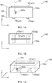
- Figures 1A-1C schematically illustrates an apparatus 100 comprising: a first layer 101 comprising a sensor 101a(1), wherein the sensor is configured to be responsive to changes in an electric field in the vicinity of the sensor; a second layer 102 comprising a substrate 102a configured to produce charge carriers 102b in response to incident radiation 104; and a third layer 103 comprising a plurality of electrodes 103a(1)-103a(j), wherein the plurality of electrodes are configured to be selectively addressed during a readout operation of the sensor.
- the sensor 101a(1) may comprise one or more means, components or devices that are responsive to changes in an electric field in the vicinity of the sensor, i.e. sensitive to local electric field perturbations (such as those caused by the production of charge carriers 102b in the substrate 102a of the second layer 102 in response to incident radiation 104).
- the sensor may be elongate.
- the sensor may comprise a material configured to be responsive to changes in an electric field in the vicinity of the material, for example such that a resistance of the material is dependent on a local electric field.
- the material may be a two-dimensional material, not least for example graphene.
- the sensor may comprise a transistor, such as a field effect transistor. In certain examples, the sensor comprises a graphene field effect transistor (GFET).
- the sensor may comprise an elongate strip of material provided between two electrodes, such electrodes being used to perform a readout operation of the elongate sensor to measure the sensor's response to perturbations in the local electric field.
- the second layer 102 may be disposed between the first and third layers 101 and 103.
- the substrate 102a of the second layer 102 may be formed of a means, for example a semiconductor, not least for example such as CdTe (Cadmium Telluride), SiC (Silicon Carbide) or GaAs (Galium Arsenide) or any other suitable material offering high efficiency in capturing radiation (such as x-rays) and producing charge carriers, such as free electron-hole pairs.
- the substrate 102a may be formed of a semiconductor material having high atomic number (z).
- the third layer 103 and the substrate 102a may be provided with a thickness of the order of, for example, 0.1, 0.5, 1, 3, 5 and 10mm. Utilizing substrates formed of materials with high atomic numbers advantageously may provide increased radiation capturing depths and thus increased detection efficiency, particularly in medical applications with x-rays of 10-200keV energy range.
- the plurality of electrodes/selectively addressable means 103a(1)-103a(j) may be configured to generate an electric field which causes one or more of the charge carriers of the substrate layer to drift towards the electrode and oppositely charged charge carriers to drift towards to the sensor (thereby altering the electric field in the vicinity of the sensor, which the sensor is able to detect).
- the plurality of electrodes, or means for generating such an electric field may be disposed laterally side-by-side one another underneath the substrate/second layer.
- the plurality of electrodes may also be positioned such that they are transversely aligned (e.g. in a cross-wise) with respect to the sensor.
- the electrodes may underlie the sensor so as to be laterally spaced apart along the length of the sensor lying (indirectly) beneath the sensor.
- Examples of the apparatus are able to detect incident radiation by sensing a change in the electric field in the vicinity of the elongate sensor caused by the creation of charge carriers in the substrate in response to exposure to radiation. Such detection may be considered to correspond to 'direct' detection of radiation as compared to, for example, scintillator based detection where an intermediary conversion of the incident radiation to light occurs which is then itself detected.
- Figure 2 shows an apparatus 200 similar to the apparatus 100 with the addition of circuitry 201 configured to monitor one or more parameters of one or more responses of the sensor whilst the plurality of electrodes are selectively addressed.
- the sensor 101a(1) comprises a first electrode 101b(1), a second electrode 101c(1) and a material 101d(1) provided between the first and second electrodes 101b(1) and 101c(1).
- the material 101d(1) is configured to be sensitive to electric fields.
- the sensor may be elongate.
- the material may comprise a strip or channel of graphene.
- the first and second electrodes and the material may form at least part of a transistor, not least for example a field effect transistor.
- the first and second electrodes and the material form at least part of a GFET.
- the first and second electrodes may be configured to provide source and drain electrodes.
- the plurality of electrodes may be configured to provide a plurality of gate electrodes.
- the circuitry 201 of Figure 2 may comprise one or more of monitoring, control and readout circuitry.
- the parameters of the one or more responses of the elongate sensor may, in certain examples, correspond to a resistance of the sensor.
- the circuitry 201 may monitor a voltage drop across the electrodes 101b(1) - 101c(1) and/or current passing therebetween.
- the circuitry 201 may be galvanically connected with the first and second electrodes 101b(1) and 101c(1) via control/readout lines 202 and 203. Furthermore, control/addressing lines 204(1)-204(j) may be provided to galvanically connect the circuitry 201 to the plurality of electrodes 103a(1)-103a(j).
- the circuitry 201 may be configured to control the readout operation of the elongate sensor whilst sequentially applying an input voltage to each of the plurality of electrodes.
- the control circuitry may be configured to measure one or more responses of the elongate sensor upon the provision of an input to each of the plurality of electrodes.
- detection of radiation occurs via the sensor's sensitivity to local electric field perturbations caused by ionised charges generated in the adjacent substrate.
- radiation is incident to the apparatus 200 proximal to a particular one of the plurality of electrodes 103a(1)-103a(j)
- the applied voltage causes the created charge carriers (electron-hole pairs) to separate and drift towards the particular electrode and the material 101d(1). This causes a perturbance in the electric field in the vicinity of the material which is sensed by the material and causes a response, such as affecting its resistance.
- the magnitude of the response when the particular electrode is addressed/applied with an input voltage is greater than the magnitude of the response when another of the plurality of electrodes (such as one less proximal to the site of the incident radiation) is addressed/applied with an input voltage.
- another of the plurality of electrodes such as one less proximal to the site of the incident radiation
- a determination can be made as to the electrode most proximal to the location of the incident radiation.
- identifying the particular electrode most proximal to the site of incident radiation a determination can then be made as to the location on the apparatus of the incident, thereby providing position sensitive detection of the radiation.
- the control circuitry may be configured to:
- Figure 3 illustrates a further apparatus 300 that is configured so as to additionally enable position sensitive detection of incident radiation 104 in a transverse direction (i.e. Y direction) and which may therefore be used, in combination with the above-described position sensitivity in the longitudinal direction, to provide two-dimensional position sensitivity for the apparatus 300.
- a transverse direction i.e. Y direction
- the first layer 101 comprises a plurality of sensors 101a(1)-101a(i) which may be connected to the circuitry 301 via respective control/readout lines 202(1)-202(i) and 203(1)-203(i).
- Each of the elongate sensors is configured to extend in a first direction, i.e. a longitudinal X direction.
- Each of the plurality of electrodes 103a(1)-103a(j) of the third layer 103 is configured to extend in a second direction, substantially perpendicular to the first direction, i.e. a transverse "Y" direction.
- Each of the plurality of electrodes may themselves be elongate such that they extend beneath each of the plurality of sensors 101a(1)-101a(i) of the first layer 101. Such a configuration may provide a 'cross-bar' geometry sensor arrangement.
- the plurality of sensors may be provided in a first arrangement, i.e. provided in a spaced apart, side-by side and parallel array.
- the plurality of electrodes may be provided in a second arrangement, which may be substantially perpendicular to the arrangement of the first array, e.g. a plurality of spaced apart, side-by-side elongate electrodes in parallel but perpendicular to the parallel elongate sensors of the first layer.
- the circuitry 301 may be configured to monitor one or more parameters of the one or more responses of the plurality of elongate sensors, not least for example the resistivity of the sensors. This may be achieved by measuring the voltage across and/or current passing through each respective first and second electrode pair, 101b(1) and 101c(1) - 101 b(i) and 101c(i), of each of the plurality of sensors, 101a(1)-(i).
- the circuitry 301 may measure one or more responses of each of the plurality of elongate sensors and, using the same, may then:
- the ability to provide such position sensitive detection in a transverse direction of the apparatus 300 in combination with the ability to provide position sensitive detection of incident radiation 104 in a perpendicular longitudinal direction of the apparatus may provide the ability to detect the position of incident radiation over a two-dimensional surface of the apparatus. Such two-dimensional positional detection of incident radiation may enable an image of incident radiation to be captured.
- the position sensitivity/resolution in each of the X and Y directions may be increased by increasing the density of the number of sensors 101a(1)-101a(i) and electrodes 103a(1)-103a(j), i.e. the number of sensors per unit length and number of the plurality of electrodes per unit length.
- the apparatus 100, 200, 300 may be for detecting and/or imaging radiation, not least for example x-rays.
- Figure 4 shows a further apparatus 400 comprising an additional fourth layer 401 disposed above the first layer 101, wherein the fourth layer comprises a further electrode 401 a.
- the further 'top' electrode may be spaced apart from the first layer 101 via an intermediary layer 402, such as a layer of a dielectric material 402a.
- the further electrode 401 a may extend both in a longitudinal direction as well as a transverse direction so as to provide a substantially 2 dimensional planar electrode overlaying the one or more sensors of the first layer 101.
- Control circuitry 403 may be used to provide a voltage to the further electrode 401 a, via control line 410, for example providing a potential difference between the further electrode 401 a and one or more of the electrodes 103a(1)-103a(j).
- a predetermined voltage may be applied so as to increase the drift/transport velocity of the charge carriers in the substrate 102a.
- Increasing the transport/drift of the charge carriers advantageously may improve the timing properties of the detector and increasing its response time. This may broaden the possible fields of application of the apparatus 400 in medical imaging, i.e. enabling it to be used in radiography/static x-ray imaging, fluoroscopy and CT scanning, where a fast response time of a detector is required.
- electrode 401 a may additionally and/or alternatively be provided with a further voltage input for neutralising any trapped charges in the apparatus so as to effectively provide a reset/clearance function for the apparatus 400.
- some charge carriers may get trapped in the vicinity of various of the layers of the apparatus. The trapped charges may slow down the drift velocity and reduce the readout speed of the apparatus.
- the electrode 401 a may operate as a "clearance" electrode by applying a voltage electric pulse to neutralise the trapped charges and make the apparatus ready for the next incident radiation detection event.
- clearance/reset functionality may improve the sampling rate of the apparatus and, again, broaden the possible applications of its use in areas where fast response times are required, such as CT x-ray scanners.
- Figures 5A and 5B show a cross-sectional side view and a perspective view of a further apparatus 500.
- the apparatus 500 is based on a radiation detection mechanism that does not involve a scintillator and may directly detect incident radiation 104 without requiring an intermediary converting step of the radiation to light which is itself detected (which introduces losses in intrinsic efficiency as well as effecting the positioning accuracy and spatial resolution of the detected radiation).
- the apparatus 500 is configured for direct x-ray detection based on charge sensitive GFETs and the high sensitivity of graphene resistivity on local electric field perturbations, not least those caused by ionised charges generated in the vicinity of the graphene as discussed below.
- a plurality of GFET radiation sensors (GR) 101a(1)-101a(n) each configured as a field effect transistor are provided on a radiation absorbing substrate 102a.
- the radiation technique employed is based on measurement of the electric field changes in the vicinity of the graphene channel of the GFET due to ionisations in the substrate 102a caused by incident x-rays.
- the plurality of electrodes 103a(1)-103a(j) provide a plurality of back gate electrodes.
- a back gate voltage VBY(j) is sequentially applied across the plurality of back gate electrodes.
- source and drain voltages VSX(i) and VDX(i) are applied to the plurality of first electrodes 101b(1)-101b(n) and the plurality of second electrodes 101c(1)-101c(n), so as to drift electrons or holes induced by the incident radiation 104 to the neighbourhood of the graphene channels 101d(i).
- Graphene resistivity which is highly sensitive to local electric field changes, is modified by the electric field perturbations caused by these charges.
- Each GFET radiation sensor GX(i) may provide detection as well as signal amplification jointly and may enable the sensing of radiation with high sensitivity, low noise and low power consumption at room temperature.
- the apparatus 500 is made from a plurality of GFET transistors (GI) on a semiconductor substrate.
- the GFET transistors are provided with elongate graphene strips placed parallel to a Y direction, wherein each strip is terminated by a pair of electrodes, namely a first and second electrode 101b(n) and 101c(n), for example made of Au.
- Positional sensitivity in the X direction is achieved by the placement of each graphene strip, i.e. the X coordinate of the graphene strip.
- Positional sensitivity in a perpendicular X direction is provided by the gate electrodes placed at the bottom of the substrate 103a(n) aligned perpendicularly to direction Y.
- Each GFET transistor is sequentially addressed by an array of gate and source electrodes 101b(n), 101 c(n) with respective gate-source voltages VBY(j)-VSX(i).
- Such an arrangement and architecture of gate electrodes and graphene strips form a crossbar readout system which enables the possibility for sequentially reading each localised interaction point (i.e. a point where radiation interacts with the substrate so as to produce an electron-hole pair) across the two-dimensional coordinates, X-Y, of the substrate 102a, thereby enabling localised detection of an incident x-ray event in the substrate.
- Such positional sensitivity may enable the formation of an x-ray image.
- Figure 5B illustrates a partially exploded perspective view of the apparatus 500 showing an upper electrode 401 a, which, as discussed with regards to Figure 4 , may function as a drift electrode and/or reset/clearance electrode so as to increase the speed of drift of generated localised electron-hole pairs and also to enable the discharging of any trapped charges after a certain period of operation.
- a dielectric 402a is provided between the top electrode 401 a and the layer comprising the source electrodes, graphene strips and drain electrodes.
- the substrate 102a may have a thickness several orders or magnitude greater than the thickness of other layers and electrodes, and may be of the order of mm thick.
- the substrate may be made from a heavy semiconductor material such as CdTe, SiC, GaAs.
- Lines 501 illustrate an electric field between the top electrode 401 a and the bottom gate electrode 103a(j).
- the top electrode 401 a is provided at an upper surface of the detector.
- the top electrode 401 a may be made of a thin metallic film (for example 100nm Au for example, or transparent ITO) and may be deposited on an intermediary layer 410 comprising, for example, as thin dielectric substrate 410a(e.g. Al 2 O 3 or HFO) so as to avoid galvanic contact between the graphene strips 101d(i) yet provide high electric field transmittance.
- the GFET sensors are influenced by localised e-h pairs via the drift towards the electrodes, thereby changing the conductivity and resistance of the graphene sensors which is detected and measured.
- the top electrode 401 a may additionally function as a "clearance" electrode by applying a short inverted voltage electric pulse (-VTG) to neutralise the trapped charges and make the system ready for the next x-ray detection event.
- -VTG short inverted voltage electric pulse
- the charges are drifted towards the top electrode 401 a and the bottom gate electrodes 103a(j) by applying a voltage between the electrodes of VTG.
- the movement of the charges influences the electric field in the vicinity of the graphene strips of the GFET.
- the apparatus 500 may be read sequentially via the crossbar electrode perpendicularly placed at the top and bottom of the substrate 102a, namely the plurality of first and second electrodes 101 b(i) and 101 c(i) on the top of the substrate and the plurality of electrodes 103a(j) at the bottom of the substrate.
- Coordinates of a particular radiation incident event are determined by proximity of the electron-hole pairs to the nearest crossing point of the perpendicular graphene channels and bottom electrodes.
- the sampling rate of the apparatus 500 may be improved by introducing clearance reset inverted pulses as discussed above (-VTG) at a certain frequency so as to neutralise any accumulated trapped charges in the vicinity of layers of the apparatus.
- Certain examples of the present disclosure may avoid the need for use of expensive amorphous silicon, amorphous selenium or a scintillator based detected system for the construction of x-ray flat panels and may provide a simplified apparatus for x-ray flat panels that employs a solution based material deposition technique, such as graphene and manipulation depositing technique may enable large x-ray detection over two-dimensional areas.
- a solution based material deposition technique such as graphene and manipulation depositing technique may enable large x-ray detection over two-dimensional areas.
- the efficiency of detecting may be increased as compared to previous scintillator based detection systems, thereby meaning a lower dosage of incident radiation may be required for medical imaging.
- the apparatus may be provided in the form of a device or module.
- Examples of the present disclosure provide both an apparatus comprising various elements, components, means or circuitry that provides the functionality for performing the above-described features.
- Various of the means or circuitry may be implemented as hardware, or may be implemented as software or firmware to be performed by a computer processor.
- firmware or software examples of the present disclosure may involve a computer program product including a computer readable storage structure embodying computer program instructions (i.e. the software or firmware) thereon for performing by the computer processor.
- circuitry refers to all of the following:
- circuitry would also cover an implementation of merely a processor (or multiple processors) or portion of a processor and its (or their) accompanying software and/or firmware.
- circuitry would also cover, for example and if applicable to the particular claim element, a baseband integrated circuit or applications processor integrated circuit for a mobile phone or a similar integrated circuit in a server, a cellular network device, or other network device.
- the "determining" can include, not least: calculating, computing, processing, deriving, investigating, looking up (e.g., looking up in a table, a database or another data structure), ascertaining and the like. Also, “determining” can include receiving (e.g., receiving information), accessing (e.g., accessing data in a memory) and the like. Also, “determining” can include resolving, selecting, choosing, establishing, and the like.
- references to "a/an/the” [feature, element, component, means...] are to be interpreted as “at least one” [feature, element, component, means ...] unless explicitly stated otherwise.
Landscapes
- Physics & Mathematics (AREA)
- Health & Medical Sciences (AREA)
- Life Sciences & Earth Sciences (AREA)
- General Physics & Mathematics (AREA)
- High Energy & Nuclear Physics (AREA)
- Molecular Biology (AREA)
- Spectroscopy & Molecular Physics (AREA)
- Measurement Of Radiation (AREA)
- Solid State Image Pick-Up Elements (AREA)
Priority Applications (4)
| Application Number | Priority Date | Filing Date | Title |
|---|---|---|---|
| EP16165169.0A EP3232229A1 (fr) | 2016-04-13 | 2016-04-13 | Appareil de détection de rayonnement |
| EP16206847.2A EP3232230B1 (fr) | 2016-04-13 | 2016-12-23 | Appareil de détection de rayonnement |
| PCT/FI2017/050165 WO2017178693A1 (fr) | 2016-04-13 | 2017-03-14 | Dispositif de détection de rayonnement |
| US16/092,512 US11287539B2 (en) | 2016-04-13 | 2017-03-14 | Apparatus for sensing radiation |
Applications Claiming Priority (1)
| Application Number | Priority Date | Filing Date | Title |
|---|---|---|---|
| EP16165169.0A EP3232229A1 (fr) | 2016-04-13 | 2016-04-13 | Appareil de détection de rayonnement |
Publications (1)
| Publication Number | Publication Date |
|---|---|
| EP3232229A1 true EP3232229A1 (fr) | 2017-10-18 |
Family
ID=55752222
Family Applications (2)
| Application Number | Title | Priority Date | Filing Date |
|---|---|---|---|
| EP16165169.0A Withdrawn EP3232229A1 (fr) | 2016-04-13 | 2016-04-13 | Appareil de détection de rayonnement |
| EP16206847.2A Active EP3232230B1 (fr) | 2016-04-13 | 2016-12-23 | Appareil de détection de rayonnement |
Family Applications After (1)
| Application Number | Title | Priority Date | Filing Date |
|---|---|---|---|
| EP16206847.2A Active EP3232230B1 (fr) | 2016-04-13 | 2016-12-23 | Appareil de détection de rayonnement |
Country Status (3)
| Country | Link |
|---|---|
| US (1) | US11287539B2 (fr) |
| EP (2) | EP3232229A1 (fr) |
| WO (1) | WO2017178693A1 (fr) |
Families Citing this family (4)
| Publication number | Priority date | Publication date | Assignee | Title |
|---|---|---|---|---|
| WO2021011395A1 (fr) * | 2019-07-16 | 2021-01-21 | Georgia Tech Research Corporation | Dispositif de résistance électrique pour détection de rayonnement |
| JP7063495B1 (ja) | 2020-10-30 | 2022-05-09 | 音羽電機工業株式会社 | 電界強度を測定可能なセンサ装置 |
| US12571888B2 (en) * | 2021-05-21 | 2026-03-10 | Beijing Voyager Technology Co., Ltd. | Unified photodetector and electrode array |
| WO2025024598A1 (fr) * | 2023-07-24 | 2025-01-30 | The Regents Of The University Of California | Détection de biomarqueurs à l'aide de réseaux de capteurs à transistors à effet de champ de graphène et de l'acquisition de données multicanal |
Citations (5)
| Publication number | Priority date | Publication date | Assignee | Title |
|---|---|---|---|---|
| US6002134A (en) * | 1995-10-13 | 1999-12-14 | Digirad Corporation | Cross-strip semiconductor detector with cord-wood construction |
| CN104062676A (zh) * | 2014-05-29 | 2014-09-24 | 中国空间技术研究院 | 基于石墨烯电场效应的x射线和带电粒子探测器及探测方法 |
| US8981346B1 (en) * | 2014-09-30 | 2015-03-17 | The United States Of America As Represented By The Secretary Of The Navy | Capacitive-based graphene sensor |
| EP2876465A1 (fr) * | 2013-11-26 | 2015-05-27 | Danmarks Tekniske Universitet (DTU) | Détecteur de rayonnement gamma et de rayons X |
| WO2015107777A1 (fr) * | 2014-01-15 | 2015-07-23 | シャープ株式会社 | Détecteur de rayonnement énergétique |
Family Cites Families (34)
| Publication number | Priority date | Publication date | Assignee | Title |
|---|---|---|---|---|
| US5652430A (en) * | 1996-05-03 | 1997-07-29 | Sterling Diagnostic Imaging, Inc. | Direct radiographic imaging panel |
| US6791091B2 (en) * | 2001-06-19 | 2004-09-14 | Brian Rodricks | Wide dynamic range digital imaging system and method |
| US6727504B1 (en) * | 2001-09-28 | 2004-04-27 | Sandia National Laboratories | Boron nitride solid state neutron detector |
| US7745800B1 (en) * | 2002-12-18 | 2010-06-29 | The United States Of America As Represented By The Secretary Of The Navy | Omni-directional solid-state thermal neutron detector |
| JP2005012049A (ja) * | 2003-06-20 | 2005-01-13 | Shimadzu Corp | 放射線検出器およびそれを備えた放射線撮像装置 |
| US7233007B2 (en) * | 2004-03-01 | 2007-06-19 | Nova Scientific, Inc. | Radiation detectors and methods of detecting radiation |
| US7332726B2 (en) * | 2004-06-19 | 2008-02-19 | Integrated Sensors, Llc | Plasma panel based ionizing radiation detector |
| US7651877B2 (en) * | 2004-10-28 | 2010-01-26 | Sharp Kabushiki Kaisha | Two-dimensional image detecting apparatus and method for manufacturing the same |
| JP4750512B2 (ja) * | 2005-09-01 | 2011-08-17 | キヤノン株式会社 | 放射線撮像装置、その制御方法及び放射線撮像システム |
| US20110210262A1 (en) * | 2006-06-12 | 2011-09-01 | Radiation Watch Limited | Apparatus and method for detecting high-energy radiation |
| US7683340B2 (en) * | 2006-10-28 | 2010-03-23 | Integrated Sensors, Llc | Plasma panel based radiation detector |
| CA2615827A1 (fr) * | 2008-01-22 | 2009-07-22 | Karim S. Karim | Methode et appareil de detection de charges monopolaires pour les detecteurs de rayonnement a semiconducteurs deposes par des techniques de depot physique en phase vapeur |
| WO2010142036A1 (fr) * | 2009-06-12 | 2010-12-16 | Karim Karim S | Détecteur de rayonnement doté d'un afficheur intégré |
| US8440980B2 (en) * | 2009-08-03 | 2013-05-14 | Radiation Monitoring Devices, Inc. | CsLiLn halide scintillator |
| SG183997A1 (en) * | 2010-03-08 | 2012-10-30 | Univ Rice William M | Transparent electrodes based on graphene and grid hybrid structures |
| CN102401906B (zh) * | 2010-09-19 | 2014-03-12 | 同方威视技术股份有限公司 | 辐射探测器及其成像装置、电极结构和获取图像的方法 |
| JP5457320B2 (ja) * | 2010-09-28 | 2014-04-02 | 富士フイルム株式会社 | 放射線画像検出装置 |
| CN103261914B (zh) * | 2010-12-07 | 2016-03-23 | 皇家飞利浦电子股份有限公司 | 直接转换x射线探测器 |
| EP2883083B1 (fr) * | 2012-08-13 | 2019-02-13 | Koninklijke Philips N.V. | Détecteur de rayons x à comptage de photons |
| US9217793B2 (en) * | 2012-10-25 | 2015-12-22 | Schlumberger Technology Corporation | Apparatus and method for detecting radiation |
| WO2014087290A1 (fr) * | 2012-12-04 | 2014-06-12 | Koninklijke Philips N.V. | Détecteur de rayons x à comptage de photons |
| WO2015102746A2 (fr) * | 2013-11-04 | 2015-07-09 | Massachusetts Institute Of Technology | Composants électroniques comportant des structures hybrides à base de graphène |
| DE102014204042A1 (de) * | 2014-03-05 | 2015-09-10 | Siemens Aktiengesellschaft | Verfahren zur Ansteuerung eines Röntgendetektors und zugehörige Steuereinheit |
| US10705228B2 (en) * | 2014-06-18 | 2020-07-07 | Oregon State University | Photo sensor for use as a radiation detector and power supply and method for making and using the device |
| EP3168842B1 (fr) * | 2014-07-07 | 2020-01-29 | Toray Industries, Inc. | Panneau de scintillateur, détecteur de rayonnement et procédé de fabrication associé |
| US9696437B2 (en) * | 2014-10-31 | 2017-07-04 | The Board Of Trustees Of The Leland Stanford Junior University | Charge cloud tracker: High-resolution, high DQE, photon-counting, energy discriminating X-ray detector |
| JP6551003B2 (ja) * | 2015-07-24 | 2019-07-31 | 三菱重工業株式会社 | 放射線測定装置及び放射線測定方法 |
| US9508885B1 (en) * | 2015-09-02 | 2016-11-29 | The United States Of America As Represented By The Administrator Of The National Aeronautics And Space Administration | Graphene field effect transistor for radiation detection |
| WO2017046390A1 (fr) * | 2015-09-17 | 2017-03-23 | Koninklijke Philips N.V. | Procédé de fabrication d'un détecteur de rayonnement et détecteur de rayonnement |
| US20170108598A1 (en) * | 2015-10-14 | 2017-04-20 | Integrated Sensors, Llc | Boron based thin-film coatings |
| US9972649B2 (en) * | 2015-10-21 | 2018-05-15 | Massachusetts Institute Of Technology | Nanowire FET imaging system and related techniques |
| DE102015220793A1 (de) * | 2015-10-23 | 2017-04-27 | Siemens Healthcare Gmbh | Röntgendetektor und/oder Gammadetektor mit Lichtbias |
| JP6721682B2 (ja) * | 2015-12-03 | 2020-07-15 | コーニンクレッカ フィリップス エヌ ヴェKoninklijke Philips N.V. | 放射線検出器及び撮像装置 |
| ITUB20159390A1 (it) * | 2015-12-24 | 2017-06-24 | Fond Bruno Kessler | Rivelatore a semiconduttore, rivelatore di radiazione e apparecchiatura di rivelazione di radiazione. |
-
2016
- 2016-04-13 EP EP16165169.0A patent/EP3232229A1/fr not_active Withdrawn
- 2016-12-23 EP EP16206847.2A patent/EP3232230B1/fr active Active
-
2017
- 2017-03-14 US US16/092,512 patent/US11287539B2/en active Active
- 2017-03-14 WO PCT/FI2017/050165 patent/WO2017178693A1/fr not_active Ceased
Patent Citations (5)
| Publication number | Priority date | Publication date | Assignee | Title |
|---|---|---|---|---|
| US6002134A (en) * | 1995-10-13 | 1999-12-14 | Digirad Corporation | Cross-strip semiconductor detector with cord-wood construction |
| EP2876465A1 (fr) * | 2013-11-26 | 2015-05-27 | Danmarks Tekniske Universitet (DTU) | Détecteur de rayonnement gamma et de rayons X |
| WO2015107777A1 (fr) * | 2014-01-15 | 2015-07-23 | シャープ株式会社 | Détecteur de rayonnement énergétique |
| CN104062676A (zh) * | 2014-05-29 | 2014-09-24 | 中国空间技术研究院 | 基于石墨烯电场效应的x射线和带电粒子探测器及探测方法 |
| US8981346B1 (en) * | 2014-09-30 | 2015-03-17 | The United States Of America As Represented By The Secretary Of The Navy | Capacitive-based graphene sensor |
Non-Patent Citations (2)
| Title |
|---|
| ALEXANDER V KLEKACHEV ET AL: "Graphene Transistors and Photodetectors", INTERFACE., vol. 22, no. 1, 1 January 2013 (2013-01-01), US, pages 63 - 68, XP055237499, ISSN: 1064-8208 * |
| F. BONACCORSO ET AL: "Graphene photonics and optoelectronics", NATURE PHOTONICS, vol. 4, no. 9, 31 August 2010 (2010-08-31), pages 611 - 622, XP055089757, ISSN: 1749-4885, DOI: 10.1038/nphoton.2010.186 * |
Also Published As
| Publication number | Publication date |
|---|---|
| WO2017178693A1 (fr) | 2017-10-19 |
| US20190162866A1 (en) | 2019-05-30 |
| US11287539B2 (en) | 2022-03-29 |
| EP3232230A1 (fr) | 2017-10-18 |
| EP3232230B1 (fr) | 2022-11-09 |
Similar Documents
| Publication | Publication Date | Title |
|---|---|---|
| Bergmann et al. | 3D track reconstruction capability of a silicon hybrid active pixel detector | |
| CN111202536B (zh) | 射线探测器及其制造方法、电子设备 | |
| Zhang et al. | Progress in the development of CdZnTe unipolar detectors for different anode geometries and data corrections | |
| US8378308B2 (en) | Charged particle detectors with active detector surface for partial energy deposition of the charged particles and related methods | |
| Bolotnikov et al. | Use of the drift-time method to measure the electron lifetime in long-drift-length CdZnTe detectors | |
| US11287539B2 (en) | Apparatus for sensing radiation | |
| CN103261914A (zh) | 直接转换x射线探测器 | |
| Andreev et al. | Charge effects in dielectric films of MIS structures being under high-field injection of electrons at ionizing radiation | |
| Chaudhuri et al. | Biparametric analyses of charge trapping in Cd0. 9Zn0. 1Te based virtual Frisch grid detectors | |
| US8552429B2 (en) | Proximity charge sensing for semiconductor detectors | |
| Bolotnikov et al. | Performance studies of CdZnTe detector by using a pulse shape analysis | |
| CN102393530B (zh) | 辐射探测装置及制造方法 | |
| Kabir et al. | Determination of deep trapping states of the hole blocking layer in multilayer amorphous selenium X-ray detectors using transient dark current analysis | |
| Dinu et al. | Studies of MPPC detectors down to cryogenic temperatures | |
| Fink et al. | TCT characterization of different semiconductor materials for particle detection | |
| Krzyzanowska | Charge sharing in single-photon-counting detectors | |
| Luke et al. | Proximity charge sensing with semiconductor detectors | |
| Amman et al. | Proximity electrode signal readout of high-purity Ge detectors | |
| Camlica et al. | Performance of amorphous selenium-based unipolar charge sensing detector for photon counting x-ray imaging | |
| JP2016070752A (ja) | X線画像検出装置 | |
| Mescher et al. | Analyses on the measurement of leakage currents in CdZnTe radiation detectors | |
| Li et al. | Experimental results from an Imarad 8× 8 pixellated CZT detector | |
| JP4748567B2 (ja) | 放射線入射位置検出装置 | |
| US20110233405A1 (en) | Radiation detector | |
| Abolaban et al. | Simulation of Coplanar Proximity Charge Sensing Electrodes in CZT Detectors |
Legal Events
| Date | Code | Title | Description |
|---|---|---|---|
| PUAI | Public reference made under article 153(3) epc to a published international application that has entered the european phase |
Free format text: ORIGINAL CODE: 0009012 |
|
| AK | Designated contracting states |
Kind code of ref document: A1 Designated state(s): AL AT BE BG CH CY CZ DE DK EE ES FI FR GB GR HR HU IE IS IT LI LT LU LV MC MK MT NL NO PL PT RO RS SE SI SK SM TR |
|
| AX | Request for extension of the european patent |
Extension state: BA ME |
|
| STAA | Information on the status of an ep patent application or granted ep patent |
Free format text: STATUS: THE APPLICATION HAS BEEN WITHDRAWN |
|
| 18W | Application withdrawn |
Effective date: 20171208 |