EP3236200B1 - Procédé et dispositif d'inspection d'un substrat sur lequel des composants sont montés - Google Patents
Procédé et dispositif d'inspection d'un substrat sur lequel des composants sont montés Download PDFInfo
- Publication number
- EP3236200B1 EP3236200B1 EP15870321.5A EP15870321A EP3236200B1 EP 3236200 B1 EP3236200 B1 EP 3236200B1 EP 15870321 A EP15870321 A EP 15870321A EP 3236200 B1 EP3236200 B1 EP 3236200B1
- Authority
- EP
- European Patent Office
- Prior art keywords
- component
- shield region
- image
- shield
- region
- Prior art date
- Legal status (The legal status is an assumption and is not a legal conclusion. Google has not performed a legal analysis and makes no representation as to the accuracy of the status listed.)
- Active
Links
Images


Classifications
-
- G—PHYSICS
- G01—MEASURING; TESTING
- G01B—MEASURING LENGTH, THICKNESS OR SIMILAR LINEAR DIMENSIONS; MEASURING ANGLES; MEASURING AREAS; MEASURING IRREGULARITIES OF SURFACES OR CONTOURS
- G01B11/00—Measuring arrangements characterised by the use of optical techniques
- G01B11/02—Measuring arrangements characterised by the use of optical techniques for measuring length, width or thickness
- G01B11/06—Measuring arrangements characterised by the use of optical techniques for measuring length, width or thickness for measuring thickness ; e.g. of sheet material
- G01B11/0608—Height gauges
-
- G—PHYSICS
- G01—MEASURING; TESTING
- G01N—INVESTIGATING OR ANALYSING MATERIALS BY DETERMINING THEIR CHEMICAL OR PHYSICAL PROPERTIES
- G01N21/00—Investigating or analysing materials by the use of optical means, i.e. using sub-millimetre waves, infrared, visible or ultraviolet light
- G01N21/84—Systems specially adapted for particular applications
- G01N21/88—Investigating the presence of flaws or contamination
- G01N21/95—Investigating the presence of flaws or contamination characterised by the material or shape of the object to be examined
- G01N21/956—Inspecting patterns on the surface of objects
- G01N21/95607—Inspecting patterns on the surface of objects using a comparative method
-
- G—PHYSICS
- G01—MEASURING; TESTING
- G01N—INVESTIGATING OR ANALYSING MATERIALS BY DETERMINING THEIR CHEMICAL OR PHYSICAL PROPERTIES
- G01N21/00—Investigating or analysing materials by the use of optical means, i.e. using sub-millimetre waves, infrared, visible or ultraviolet light
- G01N21/84—Systems specially adapted for particular applications
- G01N21/88—Investigating the presence of flaws or contamination
-
- G—PHYSICS
- G01—MEASURING; TESTING
- G01B—MEASURING LENGTH, THICKNESS OR SIMILAR LINEAR DIMENSIONS; MEASURING ANGLES; MEASURING AREAS; MEASURING IRREGULARITIES OF SURFACES OR CONTOURS
- G01B11/00—Measuring arrangements characterised by the use of optical techniques
- G01B11/24—Measuring arrangements characterised by the use of optical techniques for measuring contours or curvatures
- G01B11/25—Measuring arrangements characterised by the use of optical techniques for measuring contours or curvatures by projecting a pattern, e.g. one or more lines, moiré fringes on the object
-
- G—PHYSICS
- G01—MEASURING; TESTING
- G01B—MEASURING LENGTH, THICKNESS OR SIMILAR LINEAR DIMENSIONS; MEASURING ANGLES; MEASURING AREAS; MEASURING IRREGULARITIES OF SURFACES OR CONTOURS
- G01B11/00—Measuring arrangements characterised by the use of optical techniques
- G01B11/24—Measuring arrangements characterised by the use of optical techniques for measuring contours or curvatures
- G01B11/25—Measuring arrangements characterised by the use of optical techniques for measuring contours or curvatures by projecting a pattern, e.g. one or more lines, moiré fringes on the object
- G01B11/2518—Projection by scanning of the object
- G01B11/2527—Projection by scanning of the object with phase change by in-plane movement of the patern
-
- G—PHYSICS
- G01—MEASURING; TESTING
- G01N—INVESTIGATING OR ANALYSING MATERIALS BY DETERMINING THEIR CHEMICAL OR PHYSICAL PROPERTIES
- G01N21/00—Investigating or analysing materials by the use of optical means, i.e. using sub-millimetre waves, infrared, visible or ultraviolet light
- G01N21/84—Systems specially adapted for particular applications
- G01N21/88—Investigating the presence of flaws or contamination
- G01N21/8806—Specially adapted optical and illumination features
-
- G—PHYSICS
- G01—MEASURING; TESTING
- G01N—INVESTIGATING OR ANALYSING MATERIALS BY DETERMINING THEIR CHEMICAL OR PHYSICAL PROPERTIES
- G01N21/00—Investigating or analysing materials by the use of optical means, i.e. using sub-millimetre waves, infrared, visible or ultraviolet light
- G01N21/84—Systems specially adapted for particular applications
- G01N21/88—Investigating the presence of flaws or contamination
- G01N21/95—Investigating the presence of flaws or contamination characterised by the material or shape of the object to be examined
- G01N21/956—Inspecting patterns on the surface of objects
-
- G—PHYSICS
- G06—COMPUTING OR CALCULATING; COUNTING
- G06T—IMAGE DATA PROCESSING OR GENERATION, IN GENERAL
- G06T7/00—Image analysis
- G06T7/0002—Inspection of images, e.g. flaw detection
- G06T7/0004—Industrial image inspection
-
- G—PHYSICS
- G06—COMPUTING OR CALCULATING; COUNTING
- G06T—IMAGE DATA PROCESSING OR GENERATION, IN GENERAL
- G06T7/00—Image analysis
- G06T7/0002—Inspection of images, e.g. flaw detection
- G06T7/0004—Industrial image inspection
- G06T7/0006—Industrial image inspection using a design-rule based approach
-
- G—PHYSICS
- G06—COMPUTING OR CALCULATING; COUNTING
- G06T—IMAGE DATA PROCESSING OR GENERATION, IN GENERAL
- G06T7/00—Image analysis
- G06T7/0002—Inspection of images, e.g. flaw detection
- G06T7/0004—Industrial image inspection
- G06T7/0008—Industrial image inspection checking presence/absence
-
- G—PHYSICS
- G06—COMPUTING OR CALCULATING; COUNTING
- G06T—IMAGE DATA PROCESSING OR GENERATION, IN GENERAL
- G06T7/00—Image analysis
- G06T7/50—Depth or shape recovery
- G06T7/521—Depth or shape recovery from laser ranging, e.g. using interferometry; from the projection of structured light
-
- H—ELECTRICITY
- H05—ELECTRIC TECHNIQUES NOT OTHERWISE PROVIDED FOR
- H05K—PRINTED CIRCUITS; CASINGS OR CONSTRUCTIONAL DETAILS OF ELECTRIC APPARATUS; MANUFACTURE OF ASSEMBLAGES OF ELECTRICAL COMPONENTS
- H05K13/00—Apparatus or processes specially adapted for manufacturing or adjusting assemblages of electric components
- H05K13/08—Monitoring manufacture of assemblages
-
- G—PHYSICS
- G01—MEASURING; TESTING
- G01N—INVESTIGATING OR ANALYSING MATERIALS BY DETERMINING THEIR CHEMICAL OR PHYSICAL PROPERTIES
- G01N21/00—Investigating or analysing materials by the use of optical means, i.e. using sub-millimetre waves, infrared, visible or ultraviolet light
- G01N21/84—Systems specially adapted for particular applications
- G01N21/88—Investigating the presence of flaws or contamination
- G01N21/8806—Specially adapted optical and illumination features
- G01N2021/8829—Shadow projection or structured background, e.g. for deflectometry
-
- G—PHYSICS
- G01—MEASURING; TESTING
- G01N—INVESTIGATING OR ANALYSING MATERIALS BY DETERMINING THEIR CHEMICAL OR PHYSICAL PROPERTIES
- G01N21/00—Investigating or analysing materials by the use of optical means, i.e. using sub-millimetre waves, infrared, visible or ultraviolet light
- G01N21/84—Systems specially adapted for particular applications
- G01N21/88—Investigating the presence of flaws or contamination
- G01N21/8806—Specially adapted optical and illumination features
- G01N2021/8835—Adjustable illumination, e.g. software adjustable screen
-
- G—PHYSICS
- G01—MEASURING; TESTING
- G01N—INVESTIGATING OR ANALYSING MATERIALS BY DETERMINING THEIR CHEMICAL OR PHYSICAL PROPERTIES
- G01N21/00—Investigating or analysing materials by the use of optical means, i.e. using sub-millimetre waves, infrared, visible or ultraviolet light
- G01N21/84—Systems specially adapted for particular applications
- G01N21/88—Investigating the presence of flaws or contamination
- G01N21/8851—Scan or image signal processing specially adapted therefor, e.g. for scan signal adjustment, for detecting different kinds of defects, for compensating for structures, markings, edges
- G01N2021/8887—Scan or image signal processing specially adapted therefor, e.g. for scan signal adjustment, for detecting different kinds of defects, for compensating for structures, markings, edges based on image processing techniques
-
- G—PHYSICS
- G01—MEASURING; TESTING
- G01N—INVESTIGATING OR ANALYSING MATERIALS BY DETERMINING THEIR CHEMICAL OR PHYSICAL PROPERTIES
- G01N21/00—Investigating or analysing materials by the use of optical means, i.e. using sub-millimetre waves, infrared, visible or ultraviolet light
- G01N21/84—Systems specially adapted for particular applications
- G01N21/88—Investigating the presence of flaws or contamination
- G01N21/95—Investigating the presence of flaws or contamination characterised by the material or shape of the object to be examined
- G01N21/956—Inspecting patterns on the surface of objects
- G01N2021/95638—Inspecting patterns on the surface of objects for PCB's
-
- G—PHYSICS
- G06—COMPUTING OR CALCULATING; COUNTING
- G06T—IMAGE DATA PROCESSING OR GENERATION, IN GENERAL
- G06T2207/00—Indexing scheme for image analysis or image enhancement
- G06T2207/10—Image acquisition modality
- G06T2207/10024—Color image
-
- G—PHYSICS
- G06—COMPUTING OR CALCULATING; COUNTING
- G06T—IMAGE DATA PROCESSING OR GENERATION, IN GENERAL
- G06T2207/00—Indexing scheme for image analysis or image enhancement
- G06T2207/10—Image acquisition modality
- G06T2207/10028—Range image; Depth image; 3D point clouds
-
- G—PHYSICS
- G06—COMPUTING OR CALCULATING; COUNTING
- G06T—IMAGE DATA PROCESSING OR GENERATION, IN GENERAL
- G06T2207/00—Indexing scheme for image analysis or image enhancement
- G06T2207/30—Subject of image; Context of image processing
- G06T2207/30108—Industrial image inspection
- G06T2207/30141—Printed circuit board [PCB]
Definitions
- the present invention relates to a method and an apparatus of inspecting a substrate with a component mounted thereon, and more particularly, the present invention relates to a method and an apparatus of inspecting a substrate with a shield together with a component.
- PCB printed circuit board
- the PCB includes a component such as a chip.
- An operation of inspecting a component such as the chip on the PCB is necessary to determine whether the component mounted on the PCB is defective or to judge whether a pad connected to the component is defective.
- a three-dimensional shape measuring apparatus using a grid pattern can be used. That is, by measuring the three-dimensional shape, it is checked whether the component is misaligned, whether the component is not mounted, whether the solder is over-coated, or not-coated.
- electronic devices such as smart phones have various functions. That is, in addition to basic communication functions, electronic devices such as a smart phone have additional functions for taking charge of a camera, a DMB, and a GPS function, etc.
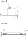
- components for performing same function are mounted being concentrated in space to form a functional block, and a shield 1000 is attached so as to surround the functional blocks respectively in order to eliminate electrical interference between the functional blocks as shown in FIG. 1 .
- the lead 11 of the component 10 which is a measurement object, is attached to the pad P formed on the substrate G by using the solder paste S.
- the solder paste S In the case of inspecting the components 10 mounted differently from each other in a state of being shielded by the edge portion 1100 of the shield 1000 as shown in FIGS. 3A and 3B , it takes a lot of time to inspect the components 10 by changing the setting for each case in judging the components 10 if the components are properly mounted.
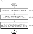
- a method of inspecting a substrate with a component mounted thereon comprises measuring a three-dimensional shape by irradiating the pattern image toward the substrate through at least one illumination unit and by taking a reflected image through an imaging unit, extracting a shield region from the three-dimensional shape, and inspecting a component mounting defect in an area excluding the shield region in the three-dimensional shape.
- extracting the shield region from the three-dimensional shape may be performed by determining a region higher than a height of the component as the shield region.
- inspecting a component mounting defect in an area excluding the shield region in the three-dimensional shape may be performed by applying an inspection condition, which is previously set, to the component under the shield region, after the component under the shied region is recognized by using at least one of CAD information and component library information.
- a method of inspecting a substrate with a component mounted thereon comprises obtaining two-dimensional image through an image capturing unit, extracting a shield region by using the two-dimensional image, and inspecting a component mounting defect in an area excluding the shield region.
- extracting a shield region by using the two-dimensional image may be performed by extracting the shield region by using at least one of brightness and color in the two-dimensional image.
- the method may further comprise measuring a three-dimensional shape by irradiating the pattern image toward the substrate through at least one illumination unit and by taking a reflected image through an imaging unit, before obtaining two-dimensional image through an image capturing unit.
- the shield region is extracted in the three-dimensional shape.
- extracting a shield region by using the two-dimensional image may be performed by further using the three-dimensional shape.
- extracting a shield region by using the two-dimensional image and the three-dimensional shape may be performed by determining a region higher than a height of the component as the shield region.
- inspecting a component mounting defect in an area excluding the shield region may be performed by applying an inspection condition, which is previously set, to the component under the shield region, after the component under the shied region is recognized by using at least one of CAD information and component library information.
- An apparatus of inspecting a substrate with a component mounted thereon comprises an image capturing unit and a central control unit.
- the image capturing unit captures an image reflected from a measurement object.
- the central control unit extracts a shield region from the image and inspects a defect of a component in an area excluding the shield region.
- the central control unit may determine a region higher than a height of the component as the shield region.
- the central control unit may apply an inspection condition, which is previously set, to the component under the shield region, after the shied region is recognized by using at least one of CAD information and component library information.
- the image capturing unit may capture a two-dimensional image
- the central control unit may determine the shield region using at least one of brightness and color of the two-dimensional image.
- the central control unit may apply an inspection condition, which is previously set, to the component under the shied region, after recognizing the component under the shield region by using at least one of CAD information and component library information in order to inspect the component mounting failure in the area excluding the shield region.
- the apparatus may further comprise an illumination unit irradiating a pattern to the measurement object.
- the image may comprise a pattern image by the pattern, and the central control unit may obtain a three-dimensional shape from the pattern image, and may extract the shield region from the three-dimensional shape.
- a non-claimed apparatus supporting a component mounting defect inspection of a substrate with a shield mounted thereon provides an interface for displaying an image obtained by an image capturing unit, provides an interface for extracting a shield region by using the image, and provides an interface for inspecting a component mounting defect in an area excluding the shield region.
- the method and the apparatus of inspecting a substrate with a component mounted thereon it is possible to judge whether the components are mounted properly or not, through the common setting without changing the setting or inspection condition, so that the inspection speed can be improved, even if the components are covered by an edge portion of a shield.
- first, second, third etc. may be used herein to describe various elements, components, regions, layers and/or sections, these elements, components, and/or sections should not be limited by these terms. These terms are only used to distinguish one element, component, region, layer or section from another region, layer or section. Thus, a first element, component, or section discussed below could be termed a second element, component, or section without departing from the teachings of the present invention.
- FIG. 4 is a conceptual diagram showing a three-dimensional shape measuring apparatus used in a three-dimensional shape measuring method according to an exemplary embodiment of the present invention.
- a three-dimensional shape measuring apparatus used in the three-dimensional shape measuring method may include a measurement stage unit 100, an image capturing unit 200, first and second illumination units 300 and 400, an image acquisition unit 500, a module control unit 600, and a central control unit 700.
- the measurement stage unit 100 may include a stage 110 for supporting a measurement object 10 and a stage transfer unit 120 for transferring the stage 110.
- a stage 110 for supporting a measurement object 10
- a stage transfer unit 120 for transferring the stage 110.
- the measurement position of measurement can be changed.
- the image capturing unit 200 is disposed over the stage 110 and receives light reflected from the measurement object 10 to measure an image of the measurement object 10. That is, the image capturing unit 200 receives the light emitted from the first and second illumination units 300 and 400 and reflected by the measurement object 10, and captures a plane image of the measurement object 10.
- the image capturing unit 200 may include a camera 210, an image forming lens 220, a filter 230 and a lamp 240.
- the camera 210 receives the light reflected from the measurement object 10 and takes a plane image of the measurement object 10.
- any one of a CCD camera and a CMOS camera may be employed.
- the image forming lens 220 is disposed below the camera 210 to image the light reflected from the measurement object 10 at the camera 210.
- the filter 230 is disposed below the image forming lens 220 to filter light reflected by the measurement object 10 and to provide the image to the image forming lens 220.
- the filter 230 may include one of frequency filter, a color filter and an intensity adjustment filter.
- the lamp 240 may be circularly arranged under the filter 230, or may be disposed separately from the image capturing unit 200, and may be composed of a plurality of LEDs.
- the lamp 240 may provide light to the measurement object 10 in order to capture a specific image such as a two-dimensional shape of the measurement object 10.
- the image capturing unit 200 may be disposed in a direction perpendicular to a plane or may be inclined with respect to a normal perpendicular to a plane.
- the image capturing unit 200 includes a plurality of image capturing units, at least one image capturing unit may be disposed in a direction perpendicular to a plane or may be inclined with respect to a normal perpendicular to a plane.
- the image capturing unit 200 may be disposed in parallel with the plane.
- the image capturing unit 200 may perform at least of capturing an image of light irradiated from the lamp 240 and reflected by the measurement object 10, and capturing a grid-patterned light irradiated from the first and second illumination units 300 and 400 and reflected by the measurement object 10.
- the first illumination unit 300 may be disposed such that the first illumination unit 300 irradiates the measurement object 10 in a direction perpendicular to the plane of the measurement object 10 or in a direction inclined with respect to the stage 110 supporting the measurement object 10 in a right side of the image capture unit 200.
- the first illumination unit 300 may include a first illumination unit 310, a first grating unit 320, a first grating transfer unit 330 and a first condensing lens 340.
- the first illumination unit 310 includes an illumination source and at least one lens to generate light.
- the first grating unit 320 is disposed below the first illumination unit 310, and transforms the light generated by the first illumination unit 310 to the first grid-patterned light having the grid pattern.
- the first grating transfer unit 330 is connected to the first grating unit 320 to transfer the first grating unit 320.
- the first grating transfer unit 330 may be a PZT (Piezoelectric) transfer unit or a fine linear transfer unit.
- the first condensing lens 340 is disposed below the first grating unit 320 to condense the first grating pattern light generated from the first grating unit 320 to the measurement object 10.
- the second illumination unit 400 may be disposed such that the second illumination unit 400 irradiates the measurement object 10 in a direction inclined with respect to the stage 110 supporting the measurement object 10 in a left side of the image capture unit 200.
- the second illumination unit 400 may include a second illumination unit 410, a second grating unit 420, a second grating transfer unit 430 and a second condensing lens 440. Since the second illuminating unit 400 is substantially the same as the first illuminating unit 300 described above, a detailed description will be omitted.
- the image capturing unit 200 may sequentially acquire N-number of first pattern images by sequentially receiving the N-number of first pattern light reflected from the measurement object 10.
- the image capturing unit 200 may sequentially acquire N-number of second pattern images by sequentially receiving the N-number of second pattern light reflected from the measurement object 10.
- N is a natural number, for example, three or four.
- the first illumination unit 300 may include a liquid crystal display device.
- the first and second illumination units 300 and 400 are described as an illumination apparatus for generating the first and second grid-patterned lights, but the number of the illumination units may be three or more. That is, the grid-patterned light may be irradiated to the measurement object 10 in various directions, and various types of pattern images may be captured. For example, when three illumination units are arranged in an equilateral triangle shape around the image capturing unit 200, three grid-patterned lights can be applied to the measurement object 10 in different directions. When four illumination units are arranged in a square shape around the image capturing unit 200, four grid-patterned lights can be applied to the measurement object 10 in different directions.
- the image acquisition unit 500 is electrically connected to the camera 210 of the image capturing unit 200, and acquires and stores the pattern images from the camera 210.
- the image acquisition unit 500 includes an image system for receiving and storing the N-number of first pattern images and the N-number of second pattern images captured by the camera 210.
- the module control unit 600 is electrically connected to the measurement stage unit 100, the image capturing unit 200, the first illuminating unit 300 and the second illuminating unit 400 to control them.
- the module control unit 600 includes, for example, an illumination controller, a grid controller, and a stage controller.
- the illumination controller controls the first and second illumination units 310 and 410 to generate light, respectively.
- the grid controller controls the first and second grating transfer units 330 and 430 to move the second grating units 320 and 420, respectively.
- the stage controller may control the stage transfer unit 120 to move the stage 110 in an up and down direction, and in a left and right direction.
- the central control unit 700 is electrically connected to the image acquisition unit 500 and the module control unit 600 to control them.
- the central control unit 700 receives the N-number of first pattern images and the N-number of second pattern images from the image system of the image acquisition unit 500, and processes the received N-number of first pattern images and the N-number of second pattern images to measure the three dimensional shape of the measurement object for inspecting mounting defects of a component, based on the three dimensional shape of the measurement object.
- the central control unit 700 may extract a shield region and recognize a component covered by the shield region.
- the central control unit 700 may control the illumination controller, the grid controller and the stage controller of the module control unit 600, respectively.
- the central control unit 700 may include an image processing board, a control board, and an interface board.
- the central control unit 700 may determine an area higher than the height of the component to be a shield region.
- the central control unit 700 may recognize the component located at the lower end of the shield region by using at least one of the CAD information and the component library information for, and then apply predetermined inspection conditions to the recognized component.
- the central control unit 700 may use at least one of the brightness and the color of the two-dimensional image captured by the image capturing unit to determine a shield region in the three-dimensional shape.
- the central control unit 700 may apply inspection conditions to the component recognized by using at least one of CAD information and component library information regarding to the component.
- FIG. 5 is a flow chart showing a method of inspecting a substrate with a component mounted thereon.
- a grid image is first irradiated through the at least one illumination unit 310 and 410 toward the substrate on which the measurement object 10 is mounted, the reflected image is captured through the image capturing unit 200, and the grid image is shifted and captured again to measure the three-dimensional shape (step S110).
- the image capturing unit 200 irradiates the measurement object 10 with the grid-patterned light that has passed through the grating units 320 and 420, and the outline of the three-dimensional shape of the measurement object 10 can be obtained through an optical triangulation method. That is, by measuring the height value corresponding to each position (X, Y) of the substrate, the entire outline of the substrate can be obtained.
- the shield region is extracted from the three-dimensional shape (step S120).
- a three-dimensional shape can be used.
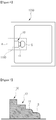
- the cross-section of the three-dimensional shape with respect to the region A in FIG. 6 can be expressed as shown in FIG. 7 .
- a region existing at a position higher than the component 10 can be judged as a shield region.
- the lamp 240 in FIG. 1 is turned on, and the coordinates (X, Y) of the edge 1100 of the shield 1000 in the two-dimensional image of FIG. 6 may be taken through the camera 210 to extract the shield region.
- the shield region can be extracted using at least one of brightness and color of the shield 1000.
- both the two-dimensional image and the three-dimensional shape may be considered to extract the shield region. If the brightness and color of the shield 1000 in the two-dimensional image is similar to the color and brightness of the substrate, it may not be easy to distinguish the shield 1000 from the substrate in the two-dimensional image. In this case, when the shield region is extracted in consideration of both the three-dimensional shape and the two-dimensional image, a more accurate shield region can be extracted.
- step S130 Thereafter, the remaining area other than the shield region is inspected if there exists mounting defects of a component.
- the portion of the component cannot be obtained in two-dimensional image or calculated in three-dimensional shape.
- the inspection condition can be applied to the corresponding component.
- the component information it is possible to check the component information to be mounted at the corresponding position through the existing CAD information and to apply the inspection condition for the component.
- both of the above methods may be applied to reflect the test conditions.
- the uncovered portion of a component may be inspected for defective mounting, such as unmount, deviation, misalignment, solder fillet, etc., based on the same inspection condition.
Landscapes
- Engineering & Computer Science (AREA)
- Physics & Mathematics (AREA)
- General Physics & Mathematics (AREA)
- Computer Vision & Pattern Recognition (AREA)
- Theoretical Computer Science (AREA)
- Biochemistry (AREA)
- Analytical Chemistry (AREA)
- Life Sciences & Earth Sciences (AREA)
- General Health & Medical Sciences (AREA)
- Immunology (AREA)
- Pathology (AREA)
- Chemical & Material Sciences (AREA)
- Health & Medical Sciences (AREA)
- Quality & Reliability (AREA)
- Operations Research (AREA)
- Manufacturing & Machinery (AREA)
- Microelectronics & Electronic Packaging (AREA)
- Optics & Photonics (AREA)
- Length Measuring Devices By Optical Means (AREA)
Claims (12)
- Procédé destiné à inspecter un substrat sur lequel un composant est monté, consistant à :obtenir au moins un élément parmi une image en deux dimensions du substrat et une forme en trois dimensions du substrat, lorsque la forme en trois dimensions est mesurée en irradiant l'image d'un motif vers le substrat par le biais d'au moins une unité d'éclairage (310, 410) et en prenant une image réfléchie par le biais d'une unité d'imagerie,caractérisé en ce que le procédé consiste en outre à :extraire une région de blindage à partir d'au moins un élément parmi l'image en deux dimensions et la forme en trois dimensions, où la région de blindage correspond à une région telle que l'état de montage du composant est caché par une portion de tranche (1100) d'un blindage (1000) pour améliorer la fonction de blindage contre les ondes électromagnétiques, etinspecter un défaut de montage de composant dans une zone excluant la région de blindage.
- Procédé selon la revendication 1, dans lequel l'extraction de la région de blindage à partir de la forme en trois dimensions est réalisée en déterminant une région plus haute qu'une hauteur du composant comme la région de blindage.
- Procédé selon la revendication 1, dans lequel l'inspection d'un défaut de montage de composant dans une zone excluant la région de blindage est réalisée en appliquant une condition d'inspection, qui est préalablement définie, au composant sous la région de blindage, après que le composant sous la région de blindage ait été reconnu en utilisant au moins un élément parmi des informations de CAO et des informations de bibliothèque de composants.
- Procédé selon la revendication 1, dans lequel l'image en deux dimensions du substrat est obtenue par le biais d'une unité de capture d'images (200).
- Procédé selon la revendication 1, dans lequel l'extraction d'une région de blindage en utilisant l'image en deux dimensions est réalisée par extraction de la région de blindage en utilisant au moins un élément parmi la luminosité et la couleur dans l'image en deux dimensions.
- Procédé selon la revendication 1, dans lequel la région de blindage est extraite en utilisant à la fois l'image en deux dimensions et la forme en trois dimensions.
- Dispositif destiné à inspecter un substrat sur lequel un composant est monté, comprenant :une unité de capture d'images (200) qui est configurée pour capturer une image réfléchie à partir d'un objet de mesure (10),caractérisé en ce que le dispositif comprend en outre :
une unité de commande centrale (700) qui est configurée pour extraire une région de blindage à partir de l'image et inspecter un défaut d'un composant dans une zone excluant la région de blindage, où la région de blindage correspond à une région telle que l'état de montage du composant est caché par une portion de tranche (1100) d'un blindage (1000) pour améliorer la fonction de blindage contre les ondes électromagnétiques. - Dispositif selon la revendication 7, dans lequel l'unité de commande centrale (700) est configurée pour déterminer une région plus haute qu'une hauteur du composant comme la région de blindage.
- Dispositif selon la revendication 7, dans lequel l'unité de commande centrale (700) est configurée pour appliquer une condition d'inspection, qui est préalablement définie, au composant sous la région de blindage, après que la région de blindage ait été reconnue en utilisant au moins un élément parmi des informations de CAO et des informations de bibliothèque de composants.
- Dispositif selon la revendication 7, dans lequel l'unité de capture d'images (200) est configurée pour capturer une image en deux dimensions, et
l'unité de commande centrale (700) est configurée pour déterminer la région de blindage en utilisant au moins un élément parmi la luminosité et la couleur de l'image en deux dimensions. - Dispositif selon la revendication 7, dans lequel l'unité de commande centrale (700) est configurée pour appliquer une condition d'inspection, qui est préalablement définie, au composant sous la région de blindage, après reconnaissance du composant sous la région de blindage en utilisant au moins un élément parmi des informations de CAO et des informations de bibliothèque de composants afin d'inspecter la défaillance de montage de composant dans la zone excluant la région de blindage.
- Dispositif selon la revendication 7, comprenant en outre une unité d'éclairage (310, 410) irradiant un motif sur l'objet de mesure (810),
dans lequel l'image comprend une image de motif par le motif, and
dans lequel l'unité de commande centrale (700) est configurée pour obtenir une forme en trois dimensions à partir de l'image de motif, et pour extraire la région de blindage à partir de la forme en trois dimensions.
Applications Claiming Priority (2)
| Application Number | Priority Date | Filing Date | Title |
|---|---|---|---|
| KR1020140181723A KR101622628B1 (ko) | 2014-12-16 | 2014-12-16 | 부품이 실장된 기판 검사방법 및 검사장치 |
| PCT/KR2015/013814 WO2016099154A1 (fr) | 2014-12-16 | 2015-12-16 | Procédé de contrôle et appareil de contrôle pour un substrat sur lequel des composants sont chargés |
Publications (3)
| Publication Number | Publication Date |
|---|---|
| EP3236200A1 EP3236200A1 (fr) | 2017-10-25 |
| EP3236200A4 EP3236200A4 (fr) | 2018-07-18 |
| EP3236200B1 true EP3236200B1 (fr) | 2019-09-04 |
Family
ID=56103927
Family Applications (1)
| Application Number | Title | Priority Date | Filing Date |
|---|---|---|---|
| EP15870321.5A Active EP3236200B1 (fr) | 2014-12-16 | 2015-12-16 | Procédé et dispositif d'inspection d'un substrat sur lequel des composants sont montés |
Country Status (5)
| Country | Link |
|---|---|
| US (1) | US10330609B2 (fr) |
| EP (1) | EP3236200B1 (fr) |
| KR (1) | KR101622628B1 (fr) |
| CN (2) | CN111007070A (fr) |
| WO (1) | WO2016099154A1 (fr) |
Families Citing this family (6)
| Publication number | Priority date | Publication date | Assignee | Title |
|---|---|---|---|---|
| EP3582599B1 (fr) * | 2017-02-13 | 2022-03-30 | Koh Young Technology Inc. | Appareil d'inspection de composants montés sur une carte de circuit imprimé, procédé de fonctionnement de celui-ci et support d'enregistrement lisible par ordinateur |
| KR102249225B1 (ko) | 2017-12-28 | 2021-05-10 | 주식회사 고영테크놀러지 | 기판에 삽입된 커넥터에 포함된 복수의 핀의 삽입 상태를 검사하는 방법 및 기판 검사 장치 |
| EP3761013A4 (fr) * | 2018-02-26 | 2021-05-12 | Koh Young Technology Inc | Procédé d'inspection de l'état de montage d'un composant, appareil d'inspection de carte de circuit imprimé et support d'enregistrement lisible par ordinateur |
| KR102182698B1 (ko) * | 2019-01-11 | 2020-11-24 | 한화정밀기계 주식회사 | 전자부품 인식장치 및 전자부품 인식방법 |
| CN109870466B (zh) * | 2019-01-25 | 2021-06-01 | 深圳市华星光电半导体显示技术有限公司 | 用于显示装置外围线路区匹配缺陷点与线路编号的方法 |
| WO2023170814A1 (fr) * | 2022-03-09 | 2023-09-14 | ヤマハ発動機株式会社 | Dispositif de commande pour mesure tridimensionnelle, programme de mesure tridimensionnelle, support d'enregistrement, dispositif de mesure tridimensionnelle et procédé de commande pour mesure tridimensionnelle |
Family Cites Families (21)
| Publication number | Priority date | Publication date | Assignee | Title |
|---|---|---|---|---|
| SG66545A1 (en) | 1988-05-09 | 1999-07-20 | Omron Tateisi Electronics Co | Apparatus for inspecting printed circuit boards and the like and method of operating the same |
| JPH06347232A (ja) * | 1993-06-04 | 1994-12-20 | Mitsubishi Heavy Ind Ltd | プリント基板外観検査装置 |
| KR970058512A (ko) | 1995-12-01 | 1997-07-31 | 구자홍 | 부품장착 상태 자동 검사장치 및 방법 |
| JP2004177377A (ja) * | 2002-11-29 | 2004-06-24 | Hitachi Ltd | 検査方法および検査装置 |
| JP2004340832A (ja) * | 2003-05-16 | 2004-12-02 | Matsushita Electric Ind Co Ltd | 回路基板の外観検査方法及び回路基板の外観検査装置 |
| ATE412335T1 (de) * | 2004-11-19 | 2008-11-15 | Sony Ericsson Mobile Comm Ab | Elektromagnetische abschirmung für elektrische bauteile auf einer gedrucken leiterplatte |
| JP4539355B2 (ja) | 2005-02-08 | 2010-09-08 | オムロン株式会社 | 基板検査装置並びにそのパラメータ設定方法およびパラメータ設定装置 |
| JP4563205B2 (ja) * | 2005-02-08 | 2010-10-13 | 富士機械製造株式会社 | 実装された電子部品の検査方法及び装置 |
| KR100612932B1 (ko) * | 2005-12-14 | 2006-08-14 | 주식회사 고영테크놀러지 | 3차원 형상 측정장치 및 방법 |
| KR101251372B1 (ko) * | 2008-10-13 | 2013-04-05 | 주식회사 고영테크놀러지 | 3차원형상 측정방법 |
| DE102010028894B4 (de) * | 2009-05-13 | 2018-05-24 | Koh Young Technology Inc. | Verfahren zur Messung eines Messobjekts |
| TWI467128B (zh) * | 2009-07-03 | 2015-01-01 | Koh Young Tech Inc | 用於檢查測量物件之方法(一) |
| US9091725B2 (en) * | 2009-07-03 | 2015-07-28 | Koh Young Technology Inc. | Board inspection apparatus and method |
| WO2011049190A1 (fr) * | 2009-10-24 | 2011-04-28 | 株式会社Djtech | Dispositif de test visuel et dispositif de test de soudure imprimée |
| KR101133976B1 (ko) | 2009-12-07 | 2012-04-05 | 주식회사 고영테크놀러지 | 3차원 검사방법 및 이를 이용한 3차원 검사장치 |
| KR101144749B1 (ko) | 2010-01-29 | 2012-05-24 | 주식회사 고영테크놀러지 | 소자의 불량 검사방법 |
| KR101657952B1 (ko) * | 2010-11-15 | 2016-09-20 | 주식회사 고영테크놀러지 | 기판 검사방법 |
| JP2012108012A (ja) | 2010-11-18 | 2012-06-07 | Panasonic Corp | 半田付け検査方法及び半田付け検査装置 |
| KR20130098221A (ko) | 2012-02-27 | 2013-09-04 | 주식회사 고영테크놀러지 | 기판 검사방법 |
| KR101779020B1 (ko) * | 2012-03-22 | 2017-09-18 | 한화테크윈 주식회사 | 부품 실장 방법 |
| CN104020177B (zh) * | 2014-06-26 | 2016-06-15 | 重庆大学 | 连铸坯表面缺陷双ccd扫描成像检测方法 |
-
2014
- 2014-12-16 KR KR1020140181723A patent/KR101622628B1/ko active Active
-
2015
- 2015-12-16 CN CN201911270860.6A patent/CN111007070A/zh active Pending
- 2015-12-16 US US15/536,213 patent/US10330609B2/en active Active
- 2015-12-16 WO PCT/KR2015/013814 patent/WO2016099154A1/fr not_active Ceased
- 2015-12-16 CN CN201580068879.6A patent/CN107110789B/zh active Active
- 2015-12-16 EP EP15870321.5A patent/EP3236200B1/fr active Active
Non-Patent Citations (1)
| Title |
|---|
| None * |
Also Published As
| Publication number | Publication date |
|---|---|
| EP3236200A4 (fr) | 2018-07-18 |
| CN107110789B (zh) | 2020-01-07 |
| US10330609B2 (en) | 2019-06-25 |
| CN111007070A (zh) | 2020-04-14 |
| KR101622628B1 (ko) | 2016-05-20 |
| CN107110789A (zh) | 2017-08-29 |
| WO2016099154A1 (fr) | 2016-06-23 |
| US20170363548A1 (en) | 2017-12-21 |
| EP3236200A1 (fr) | 2017-10-25 |
Similar Documents
| Publication | Publication Date | Title |
|---|---|---|
| EP3236200B1 (fr) | Procédé et dispositif d'inspection d'un substrat sur lequel des composants sont montés | |
| CN101943571B (zh) | 电路板检查装置及检查方法 | |
| US10126252B2 (en) | Enhanced illumination control for three-dimensional imaging | |
| EP2685242B1 (fr) | Dispositif d'examen visuel ayant une clarté d'image améliorée | |
| JP5411913B2 (ja) | 端子のチップ位置設定方法 | |
| KR101241175B1 (ko) | 실장기판 검사장치 및 검사방법 | |
| CN107429991B (zh) | 外观检查装置及外观检查方法 | |
| KR20110089519A (ko) | 3차원 형상 검사방법 | |
| US20140078296A1 (en) | Three-dimensional measuring apparatus | |
| KR101578056B1 (ko) | 삼차원 계측 장치 | |
| CN103547884A (zh) | 利用多重格子条纹的目视检查装置 | |
| KR20130110308A (ko) | 조인트 검사 장치 | |
| US10841561B2 (en) | Apparatus and method for three-dimensional inspection | |
| KR101245622B1 (ko) | 스테레오 비전과 격자 무늬를 이용한 비전검사장치 | |
| KR101522312B1 (ko) | Pcb 제품 검사 장치 및 이를 이용한 pcb 제품 검사 방법 | |
| KR101133976B1 (ko) | 3차원 검사방법 및 이를 이용한 3차원 검사장치 | |
| KR101684244B1 (ko) | 기판 검사방법 | |
| KR101511089B1 (ko) | Aoi 장비의 티칭 데이터 자동 생성 방법 | |
| KR101056995B1 (ko) | 3차원 형상 검사방법 | |
| KR101876391B1 (ko) | 단색광 모아레의 다채널 이미지를 이용한 3차원 검사 장치 | |
| KR101442666B1 (ko) | 복수 행의 조명부재를 포함하는 비전검사장치 | |
| KR101216453B1 (ko) | 측정대상물 검사방법 | |
| KR101133972B1 (ko) | 터미널 검사방법 | |
| KR101311255B1 (ko) | 측정대상물 검사방법 | |
| KR20110002981A (ko) | 브리지 연결불량 검출방법 |
Legal Events
| Date | Code | Title | Description |
|---|---|---|---|
| STAA | Information on the status of an ep patent application or granted ep patent |
Free format text: STATUS: THE INTERNATIONAL PUBLICATION HAS BEEN MADE |
|
| PUAI | Public reference made under article 153(3) epc to a published international application that has entered the european phase |
Free format text: ORIGINAL CODE: 0009012 |
|
| STAA | Information on the status of an ep patent application or granted ep patent |
Free format text: STATUS: REQUEST FOR EXAMINATION WAS MADE |
|
| 17P | Request for examination filed |
Effective date: 20170714 |
|
| AK | Designated contracting states |
Kind code of ref document: A1 Designated state(s): AL AT BE BG CH CY CZ DE DK EE ES FI FR GB GR HR HU IE IS IT LI LT LU LV MC MK MT NL NO PL PT RO RS SE SI SK SM TR |
|
| AX | Request for extension of the european patent |
Extension state: BA ME |
|
| DAV | Request for validation of the european patent (deleted) | ||
| DAX | Request for extension of the european patent (deleted) | ||
| RIC1 | Information provided on ipc code assigned before grant |
Ipc: G06T 7/10 20170101ALN20180607BHEP Ipc: G01N 21/956 20060101ALI20180607BHEP Ipc: G01B 11/06 20060101ALI20180607BHEP Ipc: H05K 13/08 20060101ALI20180607BHEP Ipc: G01B 11/25 20060101AFI20180607BHEP Ipc: G06T 7/521 20170101ALI20180607BHEP |
|
| A4 | Supplementary search report drawn up and despatched |
Effective date: 20180618 |
|
| GRAP | Despatch of communication of intention to grant a patent |
Free format text: ORIGINAL CODE: EPIDOSNIGR1 |
|
| STAA | Information on the status of an ep patent application or granted ep patent |
Free format text: STATUS: GRANT OF PATENT IS INTENDED |
|
| RIC1 | Information provided on ipc code assigned before grant |
Ipc: G06T 7/10 20170101ALN20190228BHEP Ipc: G01N 21/956 20060101ALI20190228BHEP Ipc: G01N 21/88 20060101ALI20190228BHEP Ipc: H05K 13/08 20060101ALI20190228BHEP Ipc: G01B 11/25 20060101AFI20190228BHEP Ipc: G06T 7/521 20170101ALI20190228BHEP Ipc: G01B 11/06 20060101ALI20190228BHEP Ipc: G06T 7/00 20170101ALI20190228BHEP |
|
| INTG | Intention to grant announced |
Effective date: 20190401 |
|
| GRAS | Grant fee paid |
Free format text: ORIGINAL CODE: EPIDOSNIGR3 |
|
| GRAA | (expected) grant |
Free format text: ORIGINAL CODE: 0009210 |
|
| STAA | Information on the status of an ep patent application or granted ep patent |
Free format text: STATUS: THE PATENT HAS BEEN GRANTED |
|
| AK | Designated contracting states |
Kind code of ref document: B1 Designated state(s): AL AT BE BG CH CY CZ DE DK EE ES FI FR GB GR HR HU IE IS IT LI LT LU LV MC MK MT NL NO PL PT RO RS SE SI SK SM TR |
|
| REG | Reference to a national code |
Ref country code: GB Ref legal event code: FG4D |
|
| REG | Reference to a national code |
Ref country code: CH Ref legal event code: EP |
|
| REG | Reference to a national code |
Ref country code: AT Ref legal event code: REF Ref document number: 1175988 Country of ref document: AT Kind code of ref document: T Effective date: 20190915 |
|
| REG | Reference to a national code |
Ref country code: DE Ref legal event code: R096 Ref document number: 602015037506 Country of ref document: DE |
|
| REG | Reference to a national code |
Ref country code: IE Ref legal event code: FG4D |
|
| REG | Reference to a national code |
Ref country code: NL Ref legal event code: MP Effective date: 20190904 |
|
| REG | Reference to a national code |
Ref country code: LT Ref legal event code: MG4D |
|
| PG25 | Lapsed in a contracting state [announced via postgrant information from national office to epo] |
Ref country code: FI Free format text: LAPSE BECAUSE OF FAILURE TO SUBMIT A TRANSLATION OF THE DESCRIPTION OR TO PAY THE FEE WITHIN THE PRESCRIBED TIME-LIMIT Effective date: 20190904 Ref country code: NO Free format text: LAPSE BECAUSE OF FAILURE TO SUBMIT A TRANSLATION OF THE DESCRIPTION OR TO PAY THE FEE WITHIN THE PRESCRIBED TIME-LIMIT Effective date: 20191204 Ref country code: BG Free format text: LAPSE BECAUSE OF FAILURE TO SUBMIT A TRANSLATION OF THE DESCRIPTION OR TO PAY THE FEE WITHIN THE PRESCRIBED TIME-LIMIT Effective date: 20191204 Ref country code: SE Free format text: LAPSE BECAUSE OF FAILURE TO SUBMIT A TRANSLATION OF THE DESCRIPTION OR TO PAY THE FEE WITHIN THE PRESCRIBED TIME-LIMIT Effective date: 20190904 Ref country code: LT Free format text: LAPSE BECAUSE OF FAILURE TO SUBMIT A TRANSLATION OF THE DESCRIPTION OR TO PAY THE FEE WITHIN THE PRESCRIBED TIME-LIMIT Effective date: 20190904 Ref country code: HR Free format text: LAPSE BECAUSE OF FAILURE TO SUBMIT A TRANSLATION OF THE DESCRIPTION OR TO PAY THE FEE WITHIN THE PRESCRIBED TIME-LIMIT Effective date: 20190904 |
|
| PG25 | Lapsed in a contracting state [announced via postgrant information from national office to epo] |
Ref country code: GR Free format text: LAPSE BECAUSE OF FAILURE TO SUBMIT A TRANSLATION OF THE DESCRIPTION OR TO PAY THE FEE WITHIN THE PRESCRIBED TIME-LIMIT Effective date: 20191205 Ref country code: RS Free format text: LAPSE BECAUSE OF FAILURE TO SUBMIT A TRANSLATION OF THE DESCRIPTION OR TO PAY THE FEE WITHIN THE PRESCRIBED TIME-LIMIT Effective date: 20190904 Ref country code: ES Free format text: LAPSE BECAUSE OF FAILURE TO SUBMIT A TRANSLATION OF THE DESCRIPTION OR TO PAY THE FEE WITHIN THE PRESCRIBED TIME-LIMIT Effective date: 20190904 Ref country code: AL Free format text: LAPSE BECAUSE OF FAILURE TO SUBMIT A TRANSLATION OF THE DESCRIPTION OR TO PAY THE FEE WITHIN THE PRESCRIBED TIME-LIMIT Effective date: 20190904 Ref country code: LV Free format text: LAPSE BECAUSE OF FAILURE TO SUBMIT A TRANSLATION OF THE DESCRIPTION OR TO PAY THE FEE WITHIN THE PRESCRIBED TIME-LIMIT Effective date: 20190904 |
|
| REG | Reference to a national code |
Ref country code: AT Ref legal event code: MK05 Ref document number: 1175988 Country of ref document: AT Kind code of ref document: T Effective date: 20190904 |
|
| PG25 | Lapsed in a contracting state [announced via postgrant information from national office to epo] |
Ref country code: EE Free format text: LAPSE BECAUSE OF FAILURE TO SUBMIT A TRANSLATION OF THE DESCRIPTION OR TO PAY THE FEE WITHIN THE PRESCRIBED TIME-LIMIT Effective date: 20190904 Ref country code: PL Free format text: LAPSE BECAUSE OF FAILURE TO SUBMIT A TRANSLATION OF THE DESCRIPTION OR TO PAY THE FEE WITHIN THE PRESCRIBED TIME-LIMIT Effective date: 20190904 Ref country code: IT Free format text: LAPSE BECAUSE OF FAILURE TO SUBMIT A TRANSLATION OF THE DESCRIPTION OR TO PAY THE FEE WITHIN THE PRESCRIBED TIME-LIMIT Effective date: 20190904 Ref country code: PT Free format text: LAPSE BECAUSE OF FAILURE TO SUBMIT A TRANSLATION OF THE DESCRIPTION OR TO PAY THE FEE WITHIN THE PRESCRIBED TIME-LIMIT Effective date: 20200106 Ref country code: RO Free format text: LAPSE BECAUSE OF FAILURE TO SUBMIT A TRANSLATION OF THE DESCRIPTION OR TO PAY THE FEE WITHIN THE PRESCRIBED TIME-LIMIT Effective date: 20190904 Ref country code: AT Free format text: LAPSE BECAUSE OF FAILURE TO SUBMIT A TRANSLATION OF THE DESCRIPTION OR TO PAY THE FEE WITHIN THE PRESCRIBED TIME-LIMIT Effective date: 20190904 Ref country code: NL Free format text: LAPSE BECAUSE OF FAILURE TO SUBMIT A TRANSLATION OF THE DESCRIPTION OR TO PAY THE FEE WITHIN THE PRESCRIBED TIME-LIMIT Effective date: 20190904 |
|
| PG25 | Lapsed in a contracting state [announced via postgrant information from national office to epo] |
Ref country code: SK Free format text: LAPSE BECAUSE OF FAILURE TO SUBMIT A TRANSLATION OF THE DESCRIPTION OR TO PAY THE FEE WITHIN THE PRESCRIBED TIME-LIMIT Effective date: 20190904 Ref country code: CZ Free format text: LAPSE BECAUSE OF FAILURE TO SUBMIT A TRANSLATION OF THE DESCRIPTION OR TO PAY THE FEE WITHIN THE PRESCRIBED TIME-LIMIT Effective date: 20190904 Ref country code: IS Free format text: LAPSE BECAUSE OF FAILURE TO SUBMIT A TRANSLATION OF THE DESCRIPTION OR TO PAY THE FEE WITHIN THE PRESCRIBED TIME-LIMIT Effective date: 20200224 Ref country code: SM Free format text: LAPSE BECAUSE OF FAILURE TO SUBMIT A TRANSLATION OF THE DESCRIPTION OR TO PAY THE FEE WITHIN THE PRESCRIBED TIME-LIMIT Effective date: 20190904 |
|
| REG | Reference to a national code |
Ref country code: DE Ref legal event code: R097 Ref document number: 602015037506 Country of ref document: DE |
|
| PLBE | No opposition filed within time limit |
Free format text: ORIGINAL CODE: 0009261 |
|
| STAA | Information on the status of an ep patent application or granted ep patent |
Free format text: STATUS: NO OPPOSITION FILED WITHIN TIME LIMIT |
|
| PG2D | Information on lapse in contracting state deleted |
Ref country code: IS |
|
| PG25 | Lapsed in a contracting state [announced via postgrant information from national office to epo] |
Ref country code: DK Free format text: LAPSE BECAUSE OF FAILURE TO SUBMIT A TRANSLATION OF THE DESCRIPTION OR TO PAY THE FEE WITHIN THE PRESCRIBED TIME-LIMIT Effective date: 20190904 Ref country code: IS Free format text: LAPSE BECAUSE OF FAILURE TO SUBMIT A TRANSLATION OF THE DESCRIPTION OR TO PAY THE FEE WITHIN THE PRESCRIBED TIME-LIMIT Effective date: 20200105 |
|
| REG | Reference to a national code |
Ref country code: CH Ref legal event code: PL |
|
| 26N | No opposition filed |
Effective date: 20200605 |
|
| REG | Reference to a national code |
Ref country code: BE Ref legal event code: MM Effective date: 20191231 |
|
| PG25 | Lapsed in a contracting state [announced via postgrant information from national office to epo] |
Ref country code: SI Free format text: LAPSE BECAUSE OF FAILURE TO SUBMIT A TRANSLATION OF THE DESCRIPTION OR TO PAY THE FEE WITHIN THE PRESCRIBED TIME-LIMIT Effective date: 20190904 Ref country code: MC Free format text: LAPSE BECAUSE OF FAILURE TO SUBMIT A TRANSLATION OF THE DESCRIPTION OR TO PAY THE FEE WITHIN THE PRESCRIBED TIME-LIMIT Effective date: 20190904 |
|
| GBPC | Gb: european patent ceased through non-payment of renewal fee |
Effective date: 20191216 |
|
| PG25 | Lapsed in a contracting state [announced via postgrant information from national office to epo] |
Ref country code: IE Free format text: LAPSE BECAUSE OF NON-PAYMENT OF DUE FEES Effective date: 20191216 Ref country code: FR Free format text: LAPSE BECAUSE OF NON-PAYMENT OF DUE FEES Effective date: 20191231 Ref country code: GB Free format text: LAPSE BECAUSE OF NON-PAYMENT OF DUE FEES Effective date: 20191216 Ref country code: LU Free format text: LAPSE BECAUSE OF NON-PAYMENT OF DUE FEES Effective date: 20191216 |
|
| PG25 | Lapsed in a contracting state [announced via postgrant information from national office to epo] |
Ref country code: BE Free format text: LAPSE BECAUSE OF NON-PAYMENT OF DUE FEES Effective date: 20191231 Ref country code: LI Free format text: LAPSE BECAUSE OF NON-PAYMENT OF DUE FEES Effective date: 20191231 Ref country code: CH Free format text: LAPSE BECAUSE OF NON-PAYMENT OF DUE FEES Effective date: 20191231 |
|
| PG25 | Lapsed in a contracting state [announced via postgrant information from national office to epo] |
Ref country code: CY Free format text: LAPSE BECAUSE OF FAILURE TO SUBMIT A TRANSLATION OF THE DESCRIPTION OR TO PAY THE FEE WITHIN THE PRESCRIBED TIME-LIMIT Effective date: 20190904 |
|
| PG25 | Lapsed in a contracting state [announced via postgrant information from national office to epo] |
Ref country code: HU Free format text: LAPSE BECAUSE OF FAILURE TO SUBMIT A TRANSLATION OF THE DESCRIPTION OR TO PAY THE FEE WITHIN THE PRESCRIBED TIME-LIMIT; INVALID AB INITIO Effective date: 20151216 Ref country code: MT Free format text: LAPSE BECAUSE OF FAILURE TO SUBMIT A TRANSLATION OF THE DESCRIPTION OR TO PAY THE FEE WITHIN THE PRESCRIBED TIME-LIMIT Effective date: 20190904 |
|
| PG25 | Lapsed in a contracting state [announced via postgrant information from national office to epo] |
Ref country code: TR Free format text: LAPSE BECAUSE OF FAILURE TO SUBMIT A TRANSLATION OF THE DESCRIPTION OR TO PAY THE FEE WITHIN THE PRESCRIBED TIME-LIMIT Effective date: 20190904 |
|
| PG25 | Lapsed in a contracting state [announced via postgrant information from national office to epo] |
Ref country code: MK Free format text: LAPSE BECAUSE OF FAILURE TO SUBMIT A TRANSLATION OF THE DESCRIPTION OR TO PAY THE FEE WITHIN THE PRESCRIBED TIME-LIMIT Effective date: 20190904 |
|
| PGFP | Annual fee paid to national office [announced via postgrant information from national office to epo] |
Ref country code: DE Payment date: 20251104 Year of fee payment: 11 |