EP3236459B1 - Abtastende treiberschaltung und anzeigevorrichtung - Google Patents
Abtastende treiberschaltung und anzeigevorrichtung Download PDFInfo
- Publication number
- EP3236459B1 EP3236459B1 EP15801308.6A EP15801308A EP3236459B1 EP 3236459 B1 EP3236459 B1 EP 3236459B1 EP 15801308 A EP15801308 A EP 15801308A EP 3236459 B1 EP3236459 B1 EP 3236459B1
- Authority
- EP
- European Patent Office
- Prior art keywords
- terminal
- switching element
- shift register
- register unit
- stage shift
- Prior art date
- Legal status (The legal status is an assumption and is not a legal conclusion. Google has not performed a legal analysis and makes no representation as to the accuracy of the status listed.)
- Active
Links
Images


Classifications
-
- G—PHYSICS
- G09—EDUCATION; CRYPTOGRAPHY; DISPLAY; ADVERTISING; SEALS
- G09G—ARRANGEMENTS OR CIRCUITS FOR CONTROL OF INDICATING DEVICES USING STATIC MEANS TO PRESENT VARIABLE INFORMATION
- G09G3/00—Control arrangements or circuits, of interest only in connection with visual indicators other than cathode-ray tubes
- G09G3/20—Control arrangements or circuits, of interest only in connection with visual indicators other than cathode-ray tubes for presentation of an assembly of a number of characters, e.g. a page, by composing the assembly by combination of individual elements arranged in a matrix no fixed position being assigned to or needed to be assigned to the individual characters or partial characters
- G09G3/22—Control arrangements or circuits, of interest only in connection with visual indicators other than cathode-ray tubes for presentation of an assembly of a number of characters, e.g. a page, by composing the assembly by combination of individual elements arranged in a matrix no fixed position being assigned to or needed to be assigned to the individual characters or partial characters using controlled light sources
- G09G3/30—Control arrangements or circuits, of interest only in connection with visual indicators other than cathode-ray tubes for presentation of an assembly of a number of characters, e.g. a page, by composing the assembly by combination of individual elements arranged in a matrix no fixed position being assigned to or needed to be assigned to the individual characters or partial characters using controlled light sources using electroluminescent panels
- G09G3/32—Control arrangements or circuits, of interest only in connection with visual indicators other than cathode-ray tubes for presentation of an assembly of a number of characters, e.g. a page, by composing the assembly by combination of individual elements arranged in a matrix no fixed position being assigned to or needed to be assigned to the individual characters or partial characters using controlled light sources using electroluminescent panels semiconductive, e.g. using light-emitting diodes [LED]
- G09G3/3208—Control arrangements or circuits, of interest only in connection with visual indicators other than cathode-ray tubes for presentation of an assembly of a number of characters, e.g. a page, by composing the assembly by combination of individual elements arranged in a matrix no fixed position being assigned to or needed to be assigned to the individual characters or partial characters using controlled light sources using electroluminescent panels semiconductive, e.g. using light-emitting diodes [LED] organic, e.g. using organic light-emitting diodes [OLED]
- G09G3/3225—Control arrangements or circuits, of interest only in connection with visual indicators other than cathode-ray tubes for presentation of an assembly of a number of characters, e.g. a page, by composing the assembly by combination of individual elements arranged in a matrix no fixed position being assigned to or needed to be assigned to the individual characters or partial characters using controlled light sources using electroluminescent panels semiconductive, e.g. using light-emitting diodes [LED] organic, e.g. using organic light-emitting diodes [OLED] using an active matrix
- G09G3/3258—Control arrangements or circuits, of interest only in connection with visual indicators other than cathode-ray tubes for presentation of an assembly of a number of characters, e.g. a page, by composing the assembly by combination of individual elements arranged in a matrix no fixed position being assigned to or needed to be assigned to the individual characters or partial characters using controlled light sources using electroluminescent panels semiconductive, e.g. using light-emitting diodes [LED] organic, e.g. using organic light-emitting diodes [OLED] using an active matrix with pixel circuitry controlling the voltage across the light-emitting element
-
- G—PHYSICS
- G09—EDUCATION; CRYPTOGRAPHY; DISPLAY; ADVERTISING; SEALS
- G09G—ARRANGEMENTS OR CIRCUITS FOR CONTROL OF INDICATING DEVICES USING STATIC MEANS TO PRESENT VARIABLE INFORMATION
- G09G3/00—Control arrangements or circuits, of interest only in connection with visual indicators other than cathode-ray tubes
- G09G3/20—Control arrangements or circuits, of interest only in connection with visual indicators other than cathode-ray tubes for presentation of an assembly of a number of characters, e.g. a page, by composing the assembly by combination of individual elements arranged in a matrix no fixed position being assigned to or needed to be assigned to the individual characters or partial characters
-
- G—PHYSICS
- G09—EDUCATION; CRYPTOGRAPHY; DISPLAY; ADVERTISING; SEALS
- G09G—ARRANGEMENTS OR CIRCUITS FOR CONTROL OF INDICATING DEVICES USING STATIC MEANS TO PRESENT VARIABLE INFORMATION
- G09G3/00—Control arrangements or circuits, of interest only in connection with visual indicators other than cathode-ray tubes
- G09G3/20—Control arrangements or circuits, of interest only in connection with visual indicators other than cathode-ray tubes for presentation of an assembly of a number of characters, e.g. a page, by composing the assembly by combination of individual elements arranged in a matrix no fixed position being assigned to or needed to be assigned to the individual characters or partial characters
- G09G3/22—Control arrangements or circuits, of interest only in connection with visual indicators other than cathode-ray tubes for presentation of an assembly of a number of characters, e.g. a page, by composing the assembly by combination of individual elements arranged in a matrix no fixed position being assigned to or needed to be assigned to the individual characters or partial characters using controlled light sources
- G09G3/30—Control arrangements or circuits, of interest only in connection with visual indicators other than cathode-ray tubes for presentation of an assembly of a number of characters, e.g. a page, by composing the assembly by combination of individual elements arranged in a matrix no fixed position being assigned to or needed to be assigned to the individual characters or partial characters using controlled light sources using electroluminescent panels
- G09G3/32—Control arrangements or circuits, of interest only in connection with visual indicators other than cathode-ray tubes for presentation of an assembly of a number of characters, e.g. a page, by composing the assembly by combination of individual elements arranged in a matrix no fixed position being assigned to or needed to be assigned to the individual characters or partial characters using controlled light sources using electroluminescent panels semiconductive, e.g. using light-emitting diodes [LED]
- G09G3/3208—Control arrangements or circuits, of interest only in connection with visual indicators other than cathode-ray tubes for presentation of an assembly of a number of characters, e.g. a page, by composing the assembly by combination of individual elements arranged in a matrix no fixed position being assigned to or needed to be assigned to the individual characters or partial characters using controlled light sources using electroluminescent panels semiconductive, e.g. using light-emitting diodes [LED] organic, e.g. using organic light-emitting diodes [OLED]
- G09G3/3266—Details of drivers for scan electrodes
-
- G—PHYSICS
- G11—INFORMATION STORAGE
- G11C—STATIC STORES
- G11C19/00—Digital stores in which the information is moved stepwise, e.g. shift registers
-
- G—PHYSICS
- G11—INFORMATION STORAGE
- G11C—STATIC STORES
- G11C19/00—Digital stores in which the information is moved stepwise, e.g. shift registers
- G11C19/18—Digital stores in which the information is moved stepwise, e.g. shift registers using capacitors as main elements of the stages
- G11C19/182—Digital stores in which the information is moved stepwise, e.g. shift registers using capacitors as main elements of the stages in combination with semiconductor elements, e.g. bipolar transistors, diodes
-
- G—PHYSICS
- G11—INFORMATION STORAGE
- G11C—STATIC STORES
- G11C19/00—Digital stores in which the information is moved stepwise, e.g. shift registers
- G11C19/28—Digital stores in which the information is moved stepwise, e.g. shift registers using semiconductor elements
-
- G—PHYSICS
- G11—INFORMATION STORAGE
- G11C—STATIC STORES
- G11C19/00—Digital stores in which the information is moved stepwise, e.g. shift registers
- G11C19/28—Digital stores in which the information is moved stepwise, e.g. shift registers using semiconductor elements
- G11C19/287—Organisation of a multiplicity of shift registers
-
- G—PHYSICS
- G09—EDUCATION; CRYPTOGRAPHY; DISPLAY; ADVERTISING; SEALS
- G09G—ARRANGEMENTS OR CIRCUITS FOR CONTROL OF INDICATING DEVICES USING STATIC MEANS TO PRESENT VARIABLE INFORMATION
- G09G2310/00—Command of the display device
- G09G2310/02—Addressing, scanning or driving the display screen or processing steps related thereto
- G09G2310/0264—Details of driving circuits
- G09G2310/0267—Details of drivers for scan electrodes, other than drivers for liquid crystal, plasma or OLED displays
-
- G—PHYSICS
- G09—EDUCATION; CRYPTOGRAPHY; DISPLAY; ADVERTISING; SEALS
- G09G—ARRANGEMENTS OR CIRCUITS FOR CONTROL OF INDICATING DEVICES USING STATIC MEANS TO PRESENT VARIABLE INFORMATION
- G09G2310/00—Command of the display device
- G09G2310/02—Addressing, scanning or driving the display screen or processing steps related thereto
- G09G2310/0264—Details of driving circuits
- G09G2310/0286—Details of a shift registers arranged for use in a driving circuit
-
- G—PHYSICS
- G09—EDUCATION; CRYPTOGRAPHY; DISPLAY; ADVERTISING; SEALS
- G09G—ARRANGEMENTS OR CIRCUITS FOR CONTROL OF INDICATING DEVICES USING STATIC MEANS TO PRESENT VARIABLE INFORMATION
- G09G2310/00—Command of the display device
- G09G2310/08—Details of timing specific for flat panels, other than clock recovery
Definitions
- the present disclosure relates to a scan driving circuit and a display device.
- a GOA (Gate driver on Array) circuit in a common display device needs to simultaneously provide scan signals of multiple pulse waveforms, for example, each pixel in an AMOLED (Active Matrix/Organic Light Emitting Diode) display device needs to be driven by three scan signals Rn, Gn, En in common (where n represents a stage number or a pixel row number of a shift register unit). While, in order to simultaneously provide scan signals of different pulse waveforms to each row of pixels, a traditional approach uses a different clock signal line to control a different GOA circuit unit respectively, to thereby generate scan signals for each type of pulse waveform in a relatively independent way.
- AMOLED Active Matrix/Organic Light Emitting Diode
- US 20060156121 A1 discloses an emission control compensates for the threshold voltage of transistors to provide uniform brightness using a plurality of emission control signal generating circuits, wherein first s1, second s2, and third s3 scan signals are input to the first emission control signal generating circuit to output a first emission control signal e1.
- US 20100188381 A1 discloses an emission control driver which includes a plurality of stages, each of the plurality of stages including an output terminal coupled to a corresponding one of the emission control lines: input terminals respectively coupled to two or more scan lines of the scan lines for generating a corresponding one of the emission control signals; an input circuit for controlling voltages at a first node and a second node corresponding to scan signals supplied from the two or more scan lines; and an output circuit coupled to the input circuit, the output circuit for controlling the corresponding one of the emission control signals according to the voltages at the first node and the second node.
- Embodiments of the present disclosure provide a scan driving circuit and a display device that can reduce wiring area of clock signal lines.
- a pulse width of the scan signals can be set by changing a numeric value of j.
- the embodiments of the present disclosure can obtain, based on one type of scan signals, another type of scan signals, that is, it achieves, with a scan driving circuit comprising one group of clock signal lines, functions achieved by a scan driving circuit that usually requires two groups of clock signal lines, wiring area is saved, amount of required logic elements is reduced, which facilitates improving resolution of the display device, enhancing yield, and reducing border width.
- Three types of scan signals shown in Figure 1 usually require at least two different GOA circuit units (for example, Rn+1 is taken as Gn, and En is generated separately), so that only two groups of clock signal lines in the wiring area occupy nearly one-third of a full width, which greatly restricts reduction of the border width.
- Figure 2 illustrates a structural block diagram of a scan driving circuit according to an embodiment of the present disclosure
- the scan driving circuit comprises a multi-stage shift register unit that outputs scan signals by stage under control of a clock signal
- the shift register unit includes an input terminal (connected to a line at the upper side of the shift registers in Figure 2 ) and an output terminal (connected to a line at the right side of the shift registers in Figure 2 ) for outputting the scan signals.
- an input terminal of a first stage shift register unit is connected to an initial scan signal line
- an input terminal of an arbitrary-stage shift register unit is connected to an output terminal of an adjacently upper-stage shift register unit, so that the scan signals can, under control or triggering of the clock signals, be transferred sequentially by stage in the shift register unit of each stage, and outputted at the output terminal of the shift register unit of each stage.
- the shift register unit described above can be implemented by referring to circuit structure of the shift register in the prior art provided by the inventor. Of course, shift register units can also be cascaded in other ways, the present disclosure makes no limitations thereto.
- the scan driving circuit further comprises a multi-stage signal generating unit, wherein an n-th stage signal generating unit is connected respectively to an output terminal of an n-th stage shift register unit and an output terminal of an (n+j)-th stage shift register unit, the n-th stage signal generating unit is configured to convert a first outputted level into a second level under triggering of a scan signal outputted by the n-th stage shift register unit, and convert an outputted second level into a first level under triggering of a scan signal outputted by the (n+j)-th stage shift register unit; the n and j both are positive integers.
- a triggering manner for the above scan signals can be multiple, such as high level triggering, low level triggering, edge triggering that is effective at a rising edge or a falling edge, and so on.
- the signal generating unit can convert an outputted first level into a second level or an outputted second level into a first level, wherein each of the first level and the second level may be one of a high level and a low level.
- Potentials of the high level and the low level discussed herein both are numeric values uniformly prescribed in an overall or partial digital logic unit, no more details repeated here.
- the above signal generating unit may be implemented by a digital logic unit or a combination thereof, and may also be implemented by a circuit with TFT (Thin Film Transistor) as basic elements.
- TFT Thin Film Transistor
- the embodiments of the present disclosure by providing the signal generating unit, take an n-th stage scan signal and an (n+j)-th stage scan signal as a trigger of scan signals of another pulse waveform (i.e., the signals outputted by the signal generating unit), so that such scan signals cause a level conversion while triggering (such as converting from a low level to a high level or from a high level to a low level), thus a pulse width of the scan signals can be set by changing a numeric value of j.
- the triggering manner adopted in the above example is edge triggering that is effective at a falling edge, likewise, it is also possible to set the phase of the signals outputted by the above signal generating signal by changing this triggering manner into other triggering manners.
- the n-th stage signal generating unit includes an edge trigger that is effective at a falling edge.
- the n-th stage signal generating unit described above includes a first edge trigger and a second edge trigger; a trigger signal input terminal of the first edge trigger is connected to the output terminal of the n-th stage shift register unit; a trigger signal input terminal of the second edge trigger is connected to the output terminal of the (n+2)-th stage shift register unit.
- the first edge trigger is configured to connect the high level to the output terminal of the n-th stage signal generating unit when a falling edge of a trigger signal arrives
- the second edge trigger is configured to connect the low level to the output terminal of the n-th stage signal generating unit when a falling edge of a trigger signal arrives.
- the signal generating units may have a different connection manner or setting manner, and may also be replaced by other units with similar functions, it belongs to a special design for a rear portion of the scan driving circuit, those skilled in the art can make adaptive adjustment according to the embodiments provided by the present disclosure and making reference to the prior art provided by the inventor, which obviously is not departing from the spirit and scope of the present disclosure.
- the embodiments of the present disclosure can obtain, based on one type of scan signals, another type of scan signals, that is, it achieves, with a scan driving circuit comprising one group of clock signal lines, functions achieved by a scan driving circuit that usually requires two groups of clock signal lines, wiring area is saved, amount of required logic elements is reduced, which facilitates improving resolution of the display device, enhancing yield, and reducing border width.
- Circuit structure of a scan driving circuit is provided below, to further explain the technical solutions of the present disclosure.
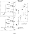
- the clock signal includes a first clock signal CKR connected to a first clock signal line and a second clock signal CKRB connected to a second clock signal line, the first clock signal CKR and the second clock signal CKR have opposite phases, thus it can be seen that this scan driving circuit requires only a pair of clock signal lines.
- the n-th stage signal generating unit described above includes:
- the n-th stage shift register unit described above includes:
- structure of the (n+1)-th stage shift register unit is the same as that of the n-th stage shift register unit (reference numerals are different), comprising: a sixth switching element T21, a seventh switching element T22, an eighth switching element T23, a ninth switching element T24, a tenth switching element T25, a third capacitor C21, a fourth capacitor C22, an input terminal (Rn at the left side of Figure 3 ), and an output terminal (Rn+1 in Figure 3 ).
- the control terminal of the sixth switching element T11, the first terminal of the seventh switching element T12, and the control terminal of the eighth switching element T13 are connected to the first clock signal line (CKR in Figure 3 )
- the second terminal of the tenth switching element T15 is connected to the second clock signal line (CKRB in Figure 3 );
- the control terminal of the sixth switching element T21, the first terminal of the seventh switching element T22, and the control terminal of the eighth switching element T23 are connected to the second clock signal line (CKRB in Figure 3 ), the second terminal of the tenth switching element T25 is connected to the first clock signal line (CKR in Figure 3 ).
- the above switching elements are electronic devices that turn on or turn off an electrical connection between the first terminal and the second terminal under control of the control terminal (turning on or turning off can be defined by a magnitude of the current that passes through, and may also be defined in a variety of ways).
- the above switching elements are a P-channel thin film transistor (TFT)
- the first terminals of the switching elements are a source of the TFT
- the second terminals of the switching elements are a drain of the TFT
- the control terminals thereof are a gate of the TFT.
- the output signal Rn-1 of an adjacent previous stage shift register unit changes from a high level to a low level, meanwhile CKR is a low level and T11 and T13 are in a turned-on state, thus gate potentials of T12 and T15 are made low, so as to turn on T12 and T15; accordingly, a gate potential of T14 also is made low, a low potential is stored in C12, thus T14 is turned on, so that the output signal Rn of this stage is made a high potential.
- CKR changes into a high level, T11 and T13 are turned off, since the potential of C12 maintains, T12 and T15 maintain turned-on, a high potential is stored into C11, and C14 is turned off, so that the output signal Rn of this stage is made a low potential.
- CKR again turns back to a low level, T11 and T13 are turned on, because Rn-1 is a high level in this case, T12 and T15 are turned off, a low potential is stored into C11, thus a gate potential of T14 is made low, T14 is turned on, the output signal Rn of this stage is made a high potential.
- the multi-stage shift register unit will complete output of the scan signals progressively in accordance with the above process, as shown by Rn-1, Rn, and Rn+1 in Figure 4 .
- n-th stage signal generating unit when Rn is a low level, CKBR also is a low level, Rn+1 is a high level, thus Ta is turned on, Tc is turned off. In this case, a gate of Tb is a low level, Tb and Te are turned on, Td is turned off, En outputs a high level of VGH.
- Rn and Rn+1 are both made a high level, due to the maintaining function of capacitors Ca and Cb, the output status of En will be maintained.
- Rn+1 is made a low level, Ta and Tc are turned on, the gate of Tb is at a high potential, in this case, Td is turned on, Tb and Te are turned off, En outputs a low level of VGL.
- the above one or more P-channel thin film transistors may be replaced with N-channel thin film transistors, in order to not change the functions of the above respective units, in this case, the following adaptive adjustment is needed: exchange the first terminal and the second terminal of the corresponding switching elements (and the source and drain wiring are interchanged), convert the high/low level of the specific signals, which is well known to those skilled in the art, details omitted.
- the display device comprises any of the scan driving circuit described above
- the display device may be: a display panel, a mobile phone, a tablet computer, a television set, a display, a notebook computer, a digital picture frame, a navigator, and any other products or components having a display function.
- the display device may be an organic light emitting diode display device, a pixel element in the OLED panel unit typically requires scan signals of multiple pulse forms to drive simultaneously, so it can uses any of the scan driving circuit described above to save wiring area, reduce amount of required logic elements, so as to improve resolution of the display device, enhance yield, and reduce border width.
- the terms “install”, “in communication”, “connect” etc. shall be interpreted broadly unless other stated and defined expressly, for example, they can relate to fixed connection or removable connection or integral connection; or can be mechanical connection or electrical connection; or can be direct connection or indirect connection via an intermediate medium; or can relate to two elements connected internally thereto.
- install in communication
- connect etc.
- install shall be interpreted broadly unless other stated and defined expressly, for example, they can relate to fixed connection or removable connection or integral connection; or can be mechanical connection or electrical connection; or can be direct connection or indirect connection via an intermediate medium; or can relate to two elements connected internally thereto.
Landscapes
- Engineering & Computer Science (AREA)
- Physics & Mathematics (AREA)
- Computer Hardware Design (AREA)
- General Physics & Mathematics (AREA)
- Theoretical Computer Science (AREA)
- Microelectronics & Electronic Packaging (AREA)
- Power Engineering (AREA)
- Control Of Indicators Other Than Cathode Ray Tubes (AREA)
Claims (6)
- Abtasttreiberschaltung, umfassend eine Mehrstufen-Schieberegistereinheit, die konfiguriert ist, Abtastsignale auszugeben mittels ihrer Stufen unter Steuerung von einem Taktsignal, umfassend ein erstes Taktsignal (CKR), zugeführt mittels einer erstes Taktsignal-Leitung, und ein zweites Taktsignal (CKBR), zugeführt mittels einer zweites Taktsignal-Leitung, wobei das erste Taktsignal und das zweite Taktsignal entgegengesetzte Phasen haben, wobei die Schieberegistereinheit Ausgangsanschlüsse beinhaltet zur Ausgabe der Abtastsignale, wobei die Abtaststeuerschaltung außerdem eine Mehrstufen-Signalerzeugungseinheit umfasst, wobei eine n-te-Stufe-Signalerzeugungseinheit der Mehrstufen-Signalerzeugungseinheit erste und zweite Eingangsanschlüsse aufweist, die an einen Ausgangsanschluss einer n-te-Stufe-Schieberegistereinheit der Mehrstufen-Schieberegistereinheit bzw. einen Ausgangsanschluss einer (n+j)-ten-Stufe-Schieberegistereinheit der Mehrstufen-Schieberegistereinheit angeschlossen sind, wobei die n-te-Stufe-Signalerzeugungseinheit einen Ausgangsanschluss aufweist, der konfiguriert ist, um einen ersten Spannungslevel oder einen zweiten Spannungslevel auszugeben, und konfiguriert ist, um einen mittels ihres Ausgangsanschlusses ausgegebenen Spannungslevel von dem ersten Spannungslevel in den zweiten Spannungslevel umzuwandeln unter Auslösung von einem Abtastsignal, ausgegeben mittels der n-te-Stufe-Schieberegistereinheit, und konfiguriert ist, um einen mittels ihres Ausgangsanschlusses ausgegebenen Spannungslevel von dem zweiten Spannungslevel in den ersten Spannungslevel umzuwandeln unter Auslösung von einem Abtastsignal, ausgegeben mittels der (n+j)-te-StufeSchieberegistereinheit; wobei das n und j beides positive Integer sind, wobei:
die n-te-Stufe-Signalerzeugungseinheit umfasst:ein erstes Schaltelement (Ta), wobei ein Steueranschluss davon angeschlossen ist an die zweites Taktsignal-Leitung, und wobei ein erster Anschluss davon angeschlossen ist an den Ausgangsanschluss der n-te-Stufe-Schieberegistereinheit,ein zweites Schaltelement (Tb), wobei ein Steueranschluss davon angeschlossen ist an einen zweiten Anschluss des ersten Schaltelements, und wobei ein erster Anschluss davon angeschlossen ist an eine Hoch-Level-Spannungsleitung (VGH) zur Zuführung des ersten Spannungslevels;ein drittes Schaltelement (Tc), wobei ein Steueranschluss davon angeschlossen ist an den Ausgangsanschluss der (n+j)-te-Stufe-Schieberegistereinheit, wobei ein erster Anschluss davon angeschlossen ist an einen zweiten Anschluss des zweiten Schaltelements, und wobei ein zweiter Anschluss davon angeschlossen ist an eine Niedrig-Level-Spannungsleitung (VHL) zum Zuführen des zweiten Spannungslevels;ein viertes Schaltelement (Td), wobei ein Steueranschluss davon angeschlossen ist an den zweiten Anschluss des zweiten Schaltelements, und wobei ein zweiter Anschluss davon angeschlossen ist an die Niedrig-Level-Spannungsleitung;ein fünftes Schaltelement (Te), wobei ein Steueranschluss davon angeschlossen ist an den zweiten Anschluss des ersten Schaltelements, wobei ein erster Anschluss davon angeschlossen ist an die Hoch-Level-Spannungsleitung, und wobei ein zweiter Anschluss davon angeschlossen an einen ersten Anschluss des vierten Schaltelements;einen ersten Kondensator (Ca), wobei ein erster Anschluss davon angeschlossen ist an die Hoch-Level-Spannungsleitung, und wobei ein zweiter Anschluss davon angeschlossen ist an den zweiten Anschluss des ersten Schaltelements;einen zweiten Kondensator (Cb), wobei ein erster Anschluss davon angeschlossen ist an den zweiten Anschluss des fünften Schaltelements, und wobei ein zweiter Anschluss davon angeschlossen ist an den zweiten Anschluss des zweiten Schaltelements; wobei der Ausgangsanschluss angeschlossen ist an den zweiten Anschluss des fünften Schaltelements. - Abtasttreiberschaltung gemäß Anspruch 1, wobei die Mehrstufen-Schieberegistereinheit außerdem einen Eingangsanschluss umfasst; wobei ein Eingangsanschluss eines erste-Stufe-Schieberegisters der Mehrstufen-Schieberegistereinheit angeschlossen ist an eine Initial-Abtastsignal-Leitung, und wobei ein Eingangsanschluss einer beliebige-Stufe-Schieberegistereinheit der Mehrstufen-Schieberegistereinheit angeschlossen ist an einen Ausgangsanschluss einer benachbarte-obere-Stufe-Schieberegistereinheit der Mehrstufen-Schieberegistereinheit.
- Abtasttreiberschaltung gemäß Anspruch 2, wobei die n-te-Stufe-Schieberegistereinheit umfasst:ein sechstes Schaltelement (T11), wobei ein erster Anschluss davon angeschlossen ist an den Eingangsanschluss der n-te-Stufe-Schieberegistereinheit;ein siebtes Schaltelement (T12), wobei ein Steueranschluss davon angeschlossen ist an einen zweiten Anschluss des sechsten Schaltelements;ein achtes Schaltelement (T13), wobei ein erster Anschluss davon angeschlossen ist an einen zweiten Anschluss des siebten Schaltelements, und wobei ein zweiter Anschluss davon angeschlossen ist an die Niedrig-Level-Spannungsleitung;ein neuntes Schaltelement (T14), wobei ein Steueranschluss davon angeschlossen ist an den zweiten Anschluss des siebten Schaltelements, und wobei ein erster Anschluss angeschlossen ist an die Hoch-Level-Spannungsleitung;ein zehntes Schaltelement (T15), wobei ein Steueranschluss davon angeschlossen ist an den zweiten Anschluss des sechsten Schaltelements, und wobei ein erster Anschluss davon angeschlossen ist an einen zweiten Anschluss des neunten Schaltelements;einen dritten Kondensator (C11), wobei ein erster Anschluss davon angeschlossen ist an die Hoch-Level-Spannungsleitung, und wobei ein zweiter Anschluss davon angeschlossen ist an den zweiten Anschluss des siebten Schaltelements;einen vierten Kondensator (C12), wobei ein erster Anschluss davon angeschlossen ist an den zweiten Anschluss des neunten Schaltelements, und wobei ein zweiter Anschluss davon angeschlossen ist an den zweiten Anschluss des sechsten Schaltelements;wobei ein Steueranschluss des sechsten Schaltelements, ein erster Anschluss des siebten Schaltelements und ein Steueranschluss des achten Schaltelements an die erstes Taktsignal-Leitung angeschlossen sind, und wobei ein zweiter Anschluss des zehnten Schaltelements an die zweites Taktsignal-Leitung angeschlossen ist; wobeider Ausgangsanschluss der n-te-Stufe-Schieberegistereinheit an den zweiten Anschluss des neunten Schaltelements angeschlossen ist;wobei eine (n+1)-te-Stufe-Schieberegistereinheit der Mehrstufen-Schieberegistereinheit, wobei es sich um die benachbarte niedrigere Stufe in Bezug auf die n-te-Stufe-Schieberegistereinheit handelt, umfasst:ein elftes Schaltelement (T21), wobei ein erster Anschluss davon angeschlossen ist an den Eingangsanschluss der (n+1)-te-Stufe-Schieberegistereinheit;ein zwölftes Schaltelement (T22), wobei ein Steueranschluss davon angeschlossen ist an einen zweiten Anschluss des elften Schaltelements;ein dreizehntes Schaltelement (T23), wobei ein erster Anschluss davon angeschlossen ist an einen zweiten Anschluss des zwölften Schaltelements, und wobei ein zweiter Anschluss davon angeschlossen ist an die Niedrig-Level-Spannungsleitung;ein vierzehntes Schaltelement (T24), wobei ein Steueranschluss davon an den zweiten Anschluss des zwölften Schaltelements angeschlossen ist, und wobei ein erster Anschluss an die Hoch-Level-Spannungsleitung angeschlossen ist;ein fünfzehntes Schaltelement (T25), wobei ein Steueranschluss davon an den zweiten Anschluss des elften Schaltelements angeschlossen ist, und wobei ein erster Anschluss davon an einen zweiten Anschluss des vierzehnten Schaltelements angeschlossen ist;einen fünften Kondensator (C21), wobei ein erster Anschluss davon an die Hoch-Level-Spannungsleitung angeschlossen ist, und wobei ein zweiter Anschluss davon an den zweiten Anschluss des zwölften Schaltelements angeschlossen ist;einen sechsten Kondensator (C22), wobei ein erster Anschluss davon an den zweiten Anschluss des vierzehnten Schaltelements angeschlossen ist, und wobei ein zweiter Anschluss davon an den zweiten Anschluss des elften Schaltelements angeschlossen ist;wobei ein Steueranschluss des elften Schaltelements, ein erster Anschluss des zwölften Schaltelements und ein Steueranschluss des dreizehnten Schaltelements an die zweites Taktsignal-Leitung angeschlossen sind, und wobei ein zweiter Anschluss des fünfzehnten Schaltelements an die erstes Taktsignal-Leitung angeschlossen ist,wobei der Ausgangsanschluss der (n+1)-te-Stufe-Schieberegistereinheit an den zweiten Anschluss des vierzehnten Schaltelements angeschlossen ist;wobei der Eingangsanschluss der (n+1)-te-Stufe-Schieberegistereinheit an den Ausgangsanschluss der n-te-Stufe-Schieberegistereinheit angeschlossen ist.
- Abtasttreiberschaltung gemäß Anspruch 3, wobei die Schaltelemente Dünnschichttransistoren sind.
- Anzeigevorrichtung, umfassend die Abtasttreiberschaltung gemäß einem der Ansprüche 1-4.
- Anzeigevorrichtung gemäß Anspruch 5, wobei die Anzeigevorrichtung eine organische-lichtemittierende-Diode-Anzeigevorrichtung ist.
Applications Claiming Priority (2)
| Application Number | Priority Date | Filing Date | Title |
|---|---|---|---|
| CN201410806187.4A CN104464595B (zh) | 2014-12-19 | 2014-12-19 | 扫描驱动电路及显示装置 |
| PCT/CN2015/076768 WO2016095382A1 (zh) | 2014-12-19 | 2015-04-16 | 扫描驱动电路及显示装置 |
Publications (3)
| Publication Number | Publication Date |
|---|---|
| EP3236459A1 EP3236459A1 (de) | 2017-10-25 |
| EP3236459A4 EP3236459A4 (de) | 2018-06-27 |
| EP3236459B1 true EP3236459B1 (de) | 2019-11-27 |
Family
ID=52910557
Family Applications (1)
| Application Number | Title | Priority Date | Filing Date |
|---|---|---|---|
| EP15801308.6A Active EP3236459B1 (de) | 2014-12-19 | 2015-04-16 | Abtastende treiberschaltung und anzeigevorrichtung |
Country Status (4)
| Country | Link |
|---|---|
| US (1) | US9711089B2 (de) |
| EP (1) | EP3236459B1 (de) |
| CN (1) | CN104464595B (de) |
| WO (1) | WO2016095382A1 (de) |
Families Citing this family (12)
| Publication number | Priority date | Publication date | Assignee | Title |
|---|---|---|---|---|
| CN104318904B (zh) * | 2014-11-20 | 2017-08-01 | 京东方科技集团股份有限公司 | 移位寄存器单元及其驱动方法、移位寄存器、显示装置 |
| CN104464595B (zh) | 2014-12-19 | 2017-02-01 | 京东方科技集团股份有限公司 | 扫描驱动电路及显示装置 |
| CN104835531B (zh) * | 2015-05-21 | 2018-06-15 | 京东方科技集团股份有限公司 | 一种移位寄存器单元及其驱动方法、移位寄存器和显示装置 |
| CN104952396B (zh) * | 2015-06-30 | 2017-10-31 | 上海天马有机发光显示技术有限公司 | 一种移位寄存器及其驱动方法 |
| KR102452523B1 (ko) * | 2015-08-27 | 2022-10-11 | 삼성디스플레이 주식회사 | 주사 구동부 |
| CN105529000B (zh) * | 2016-02-18 | 2018-01-23 | 京东方科技集团股份有限公司 | 信号生成单元、移位寄存器、显示装置及信号生成方法 |
| CN105575329B (zh) * | 2016-03-16 | 2017-12-01 | 京东方科技集团股份有限公司 | 移位寄存器及驱动方法、驱动电路、阵列基板及显示装置 |
| CN105788508B (zh) * | 2016-05-24 | 2017-07-25 | 京东方科技集团股份有限公司 | 一种栅极驱动电路及显示面板 |
| CN106057143A (zh) * | 2016-05-30 | 2016-10-26 | 京东方科技集团股份有限公司 | 移位寄存器及其操作方法、栅极驱动电路和显示装置 |
| KR102735537B1 (ko) * | 2017-02-20 | 2024-12-02 | 삼성디스플레이 주식회사 | 스테이지 회로 및 이를 이용한 주사 구동부 |
| CN111312136B (zh) * | 2018-12-12 | 2022-01-14 | 京东方科技集团股份有限公司 | 移位寄存器单元、扫描驱动电路、驱动方法和显示装置 |
| CN117316114B (zh) * | 2023-11-08 | 2024-10-01 | 惠科股份有限公司 | 显示面板和显示装置 |
Family Cites Families (13)
| Publication number | Priority date | Publication date | Assignee | Title |
|---|---|---|---|---|
| JP3589926B2 (ja) | 2000-02-02 | 2004-11-17 | シャープ株式会社 | シフトレジスタ回路および画像表示装置 |
| KR100698239B1 (ko) | 2000-08-30 | 2007-03-21 | 엘지.필립스 엘시디 주식회사 | 쉬프트 레지스터 회로 |
| KR100574363B1 (ko) * | 2002-12-04 | 2006-04-27 | 엘지.필립스 엘시디 주식회사 | 레벨 쉬프터를 내장한 쉬프트 레지스터 |
| KR100602363B1 (ko) * | 2005-01-10 | 2006-07-18 | 삼성에스디아이 주식회사 | 발광제어구동부 및 그를 이용한 발광 표시장치 |
| JP2007178784A (ja) * | 2005-12-28 | 2007-07-12 | Oki Electric Ind Co Ltd | 駆動装置 |
| KR101040855B1 (ko) * | 2009-01-29 | 2011-06-14 | 삼성모바일디스플레이주식회사 | 발광 제어선 구동부 및 이를 이용한 유기전계발광 표시장치 |
| KR101073569B1 (ko) * | 2010-05-20 | 2011-10-14 | 삼성모바일디스플레이주식회사 | 발광 제어 구동부, 이를 이용한 발광 표시 장치, 및 발광 제어 신호 구동 방법 |
| KR101778701B1 (ko) * | 2010-08-11 | 2017-09-15 | 삼성디스플레이 주식회사 | 구동 장치 및 이를 포함하는 표시 장치 |
| CN103927960B (zh) * | 2013-12-30 | 2016-04-20 | 上海中航光电子有限公司 | 一种栅极驱动装置和显示装置 |
| CN103928001B (zh) * | 2013-12-31 | 2016-12-07 | 上海天马微电子有限公司 | 一种栅极驱动电路和显示装置 |
| CN104217764A (zh) * | 2014-08-29 | 2014-12-17 | 京东方科技集团股份有限公司 | 移位寄存器、其驱动方法、栅极驱动电路及显示装置 |
| CN104464595B (zh) * | 2014-12-19 | 2017-02-01 | 京东方科技集团股份有限公司 | 扫描驱动电路及显示装置 |
| CN204288760U (zh) * | 2014-12-19 | 2015-04-22 | 京东方科技集团股份有限公司 | 扫描驱动电路及显示装置 |
-
2014
- 2014-12-19 CN CN201410806187.4A patent/CN104464595B/zh active Active
-
2015
- 2015-04-16 US US14/897,430 patent/US9711089B2/en active Active
- 2015-04-16 WO PCT/CN2015/076768 patent/WO2016095382A1/zh not_active Ceased
- 2015-04-16 EP EP15801308.6A patent/EP3236459B1/de active Active
Non-Patent Citations (1)
| Title |
|---|
| None * |
Also Published As
| Publication number | Publication date |
|---|---|
| CN104464595A (zh) | 2015-03-25 |
| CN104464595B (zh) | 2017-02-01 |
| WO2016095382A1 (zh) | 2016-06-23 |
| EP3236459A4 (de) | 2018-06-27 |
| EP3236459A1 (de) | 2017-10-25 |
| US20160372041A1 (en) | 2016-12-22 |
| US9711089B2 (en) | 2017-07-18 |
Similar Documents
| Publication | Publication Date | Title |
|---|---|---|
| EP3236459B1 (de) | Abtastende treiberschaltung und anzeigevorrichtung | |
| US10930360B2 (en) | Shift register, driving method thereof, gate driving circuit, and display device | |
| CN109658865B (zh) | 移位寄存器单元及其驱动方法、栅极驱动电路、显示装置 | |
| CN115731839B (zh) | 显示驱动电路及显示装置 | |
| US10074330B2 (en) | Scan driver and display panel using the same | |
| US10204545B2 (en) | Gate driver and display device including the same | |
| US9892676B2 (en) | Gate driving circuit providing a matched gate driving signal, corresponding driving method, display circuit and display apparatus | |
| US9997136B2 (en) | Display circuit and driving method and display apparatus thereof | |
| US10593279B2 (en) | Display device, gate driving circuit and gate driving unit | |
| US11120720B2 (en) | Shift register unit and driving method thereof, gate driver, display panel and display device | |
| US10950322B2 (en) | Shift register unit circuit, method of driving the same, gate drive circuit, and display apparatus | |
| US10665189B2 (en) | Scan driving circuit and driving method thereof, array substrate and display device | |
| US11094389B2 (en) | Shift register unit and driving method, gate driving circuit, and display device | |
| US10878757B2 (en) | Shift register and time-sharing controlling method thereof, display panel and display apparatus | |
| EP3882901B1 (de) | Schieberegistereinheit und antriebsverfahren, gate-treiberschaltung und anzeigevorrichtung | |
| US20150002377A1 (en) | Organic light-emitting diode display panel | |
| CN111583880B (zh) | 移位寄存器单元电路及驱动方法、栅极驱动器和显示装置 | |
| TWI657424B (zh) | 主動矩陣基板、及包含其之顯示裝置 | |
| US11393402B2 (en) | OR logic operation circuit and driving method, shift register unit, gate drive circuit, and display device | |
| CN103106869B (zh) | 电平移位电路、扫描电路、显示装置和电子设备 | |
| US11217140B2 (en) | Display driver circuit | |
| JPWO2015163306A1 (ja) | アクティブマトリクス基板、及びそれを備えた表示装置 | |
| US11315497B2 (en) | Gate driving circuit and image display device including ihe same | |
| US9905181B2 (en) | Array substrate and scan driving circuit thereon | |
| US20170116921A1 (en) | Shift register unit, gate drive circuit using the same and display device using the same |
Legal Events
| Date | Code | Title | Description |
|---|---|---|---|
| STAA | Information on the status of an ep patent application or granted ep patent |
Free format text: STATUS: THE INTERNATIONAL PUBLICATION HAS BEEN MADE |
|
| PUAI | Public reference made under article 153(3) epc to a published international application that has entered the european phase |
Free format text: ORIGINAL CODE: 0009012 |
|
| STAA | Information on the status of an ep patent application or granted ep patent |
Free format text: STATUS: REQUEST FOR EXAMINATION WAS MADE |
|
| 17P | Request for examination filed |
Effective date: 20151208 |
|
| AK | Designated contracting states |
Kind code of ref document: A1 Designated state(s): AL AT BE BG CH CY CZ DE DK EE ES FI FR GB GR HR HU IE IS IT LI LT LU LV MC MK MT NL NO PL PT RO RS SE SI SK SM TR |
|
| AX | Request for extension of the european patent |
Extension state: BA ME |
|
| DAV | Request for validation of the european patent (deleted) | ||
| DAX | Request for extension of the european patent (deleted) | ||
| A4 | Supplementary search report drawn up and despatched |
Effective date: 20180525 |
|
| RIC1 | Information provided on ipc code assigned before grant |
Ipc: G11C 19/18 20060101ALI20180518BHEP Ipc: G11C 19/28 20060101ALI20180518BHEP Ipc: G09G 3/20 20060101AFI20180518BHEP Ipc: G09G 3/3266 20160101ALI20180518BHEP |
|
| GRAP | Despatch of communication of intention to grant a patent |
Free format text: ORIGINAL CODE: EPIDOSNIGR1 |
|
| STAA | Information on the status of an ep patent application or granted ep patent |
Free format text: STATUS: GRANT OF PATENT IS INTENDED |
|
| INTG | Intention to grant announced |
Effective date: 20190227 |
|
| GRAJ | Information related to disapproval of communication of intention to grant by the applicant or resumption of examination proceedings by the epo deleted |
Free format text: ORIGINAL CODE: EPIDOSDIGR1 |
|
| STAA | Information on the status of an ep patent application or granted ep patent |
Free format text: STATUS: REQUEST FOR EXAMINATION WAS MADE |
|
| GRAP | Despatch of communication of intention to grant a patent |
Free format text: ORIGINAL CODE: EPIDOSNIGR1 |
|
| STAA | Information on the status of an ep patent application or granted ep patent |
Free format text: STATUS: GRANT OF PATENT IS INTENDED |
|
| INTG | Intention to grant announced |
Effective date: 20190719 |
|
| GRAS | Grant fee paid |
Free format text: ORIGINAL CODE: EPIDOSNIGR3 |
|
| GRAA | (expected) grant |
Free format text: ORIGINAL CODE: 0009210 |
|
| STAA | Information on the status of an ep patent application or granted ep patent |
Free format text: STATUS: THE PATENT HAS BEEN GRANTED |
|
| AK | Designated contracting states |
Kind code of ref document: B1 Designated state(s): AL AT BE BG CH CY CZ DE DK EE ES FI FR GB GR HR HU IE IS IT LI LT LU LV MC MK MT NL NO PL PT RO RS SE SI SK SM TR |
|
| REG | Reference to a national code |
Ref country code: GB Ref legal event code: FG4D |
|
| REG | Reference to a national code |
Ref country code: CH Ref legal event code: EP |
|
| REG | Reference to a national code |
Ref country code: AT Ref legal event code: REF Ref document number: 1207584 Country of ref document: AT Kind code of ref document: T Effective date: 20191215 |
|
| REG | Reference to a national code |
Ref country code: DE Ref legal event code: R096 Ref document number: 602015042616 Country of ref document: DE |
|
| REG | Reference to a national code |
Ref country code: IE Ref legal event code: FG4D |
|
| REG | Reference to a national code |
Ref country code: NL Ref legal event code: MP Effective date: 20191127 |
|
| REG | Reference to a national code |
Ref country code: LT Ref legal event code: MG4D |
|
| PG25 | Lapsed in a contracting state [announced via postgrant information from national office to epo] |
Ref country code: BG Free format text: LAPSE BECAUSE OF FAILURE TO SUBMIT A TRANSLATION OF THE DESCRIPTION OR TO PAY THE FEE WITHIN THE PRESCRIBED TIME-LIMIT Effective date: 20200227 Ref country code: FI Free format text: LAPSE BECAUSE OF FAILURE TO SUBMIT A TRANSLATION OF THE DESCRIPTION OR TO PAY THE FEE WITHIN THE PRESCRIBED TIME-LIMIT Effective date: 20191127 Ref country code: SE Free format text: LAPSE BECAUSE OF FAILURE TO SUBMIT A TRANSLATION OF THE DESCRIPTION OR TO PAY THE FEE WITHIN THE PRESCRIBED TIME-LIMIT Effective date: 20191127 Ref country code: LV Free format text: LAPSE BECAUSE OF FAILURE TO SUBMIT A TRANSLATION OF THE DESCRIPTION OR TO PAY THE FEE WITHIN THE PRESCRIBED TIME-LIMIT Effective date: 20191127 Ref country code: NL Free format text: LAPSE BECAUSE OF FAILURE TO SUBMIT A TRANSLATION OF THE DESCRIPTION OR TO PAY THE FEE WITHIN THE PRESCRIBED TIME-LIMIT Effective date: 20191127 Ref country code: NO Free format text: LAPSE BECAUSE OF FAILURE TO SUBMIT A TRANSLATION OF THE DESCRIPTION OR TO PAY THE FEE WITHIN THE PRESCRIBED TIME-LIMIT Effective date: 20200227 Ref country code: GR Free format text: LAPSE BECAUSE OF FAILURE TO SUBMIT A TRANSLATION OF THE DESCRIPTION OR TO PAY THE FEE WITHIN THE PRESCRIBED TIME-LIMIT Effective date: 20200228 Ref country code: LT Free format text: LAPSE BECAUSE OF FAILURE TO SUBMIT A TRANSLATION OF THE DESCRIPTION OR TO PAY THE FEE WITHIN THE PRESCRIBED TIME-LIMIT Effective date: 20191127 |
|
| PG25 | Lapsed in a contracting state [announced via postgrant information from national office to epo] |
Ref country code: IS Free format text: LAPSE BECAUSE OF FAILURE TO SUBMIT A TRANSLATION OF THE DESCRIPTION OR TO PAY THE FEE WITHIN THE PRESCRIBED TIME-LIMIT Effective date: 20200327 Ref country code: HR Free format text: LAPSE BECAUSE OF FAILURE TO SUBMIT A TRANSLATION OF THE DESCRIPTION OR TO PAY THE FEE WITHIN THE PRESCRIBED TIME-LIMIT Effective date: 20191127 Ref country code: RS Free format text: LAPSE BECAUSE OF FAILURE TO SUBMIT A TRANSLATION OF THE DESCRIPTION OR TO PAY THE FEE WITHIN THE PRESCRIBED TIME-LIMIT Effective date: 20191127 |
|
| PG25 | Lapsed in a contracting state [announced via postgrant information from national office to epo] |
Ref country code: AL Free format text: LAPSE BECAUSE OF FAILURE TO SUBMIT A TRANSLATION OF THE DESCRIPTION OR TO PAY THE FEE WITHIN THE PRESCRIBED TIME-LIMIT Effective date: 20191127 |
|
| PG25 | Lapsed in a contracting state [announced via postgrant information from national office to epo] |
Ref country code: DK Free format text: LAPSE BECAUSE OF FAILURE TO SUBMIT A TRANSLATION OF THE DESCRIPTION OR TO PAY THE FEE WITHIN THE PRESCRIBED TIME-LIMIT Effective date: 20191127 Ref country code: PT Free format text: LAPSE BECAUSE OF FAILURE TO SUBMIT A TRANSLATION OF THE DESCRIPTION OR TO PAY THE FEE WITHIN THE PRESCRIBED TIME-LIMIT Effective date: 20200419 Ref country code: EE Free format text: LAPSE BECAUSE OF FAILURE TO SUBMIT A TRANSLATION OF THE DESCRIPTION OR TO PAY THE FEE WITHIN THE PRESCRIBED TIME-LIMIT Effective date: 20191127 Ref country code: ES Free format text: LAPSE BECAUSE OF FAILURE TO SUBMIT A TRANSLATION OF THE DESCRIPTION OR TO PAY THE FEE WITHIN THE PRESCRIBED TIME-LIMIT Effective date: 20191127 Ref country code: RO Free format text: LAPSE BECAUSE OF FAILURE TO SUBMIT A TRANSLATION OF THE DESCRIPTION OR TO PAY THE FEE WITHIN THE PRESCRIBED TIME-LIMIT Effective date: 20191127 Ref country code: CZ Free format text: LAPSE BECAUSE OF FAILURE TO SUBMIT A TRANSLATION OF THE DESCRIPTION OR TO PAY THE FEE WITHIN THE PRESCRIBED TIME-LIMIT Effective date: 20191127 |
|
| REG | Reference to a national code |
Ref country code: DE Ref legal event code: R097 Ref document number: 602015042616 Country of ref document: DE |
|
| PG25 | Lapsed in a contracting state [announced via postgrant information from national office to epo] |
Ref country code: SM Free format text: LAPSE BECAUSE OF FAILURE TO SUBMIT A TRANSLATION OF THE DESCRIPTION OR TO PAY THE FEE WITHIN THE PRESCRIBED TIME-LIMIT Effective date: 20191127 Ref country code: SK Free format text: LAPSE BECAUSE OF FAILURE TO SUBMIT A TRANSLATION OF THE DESCRIPTION OR TO PAY THE FEE WITHIN THE PRESCRIBED TIME-LIMIT Effective date: 20191127 |
|
| REG | Reference to a national code |
Ref country code: AT Ref legal event code: MK05 Ref document number: 1207584 Country of ref document: AT Kind code of ref document: T Effective date: 20191127 |
|
| PLBE | No opposition filed within time limit |
Free format text: ORIGINAL CODE: 0009261 |
|
| STAA | Information on the status of an ep patent application or granted ep patent |
Free format text: STATUS: NO OPPOSITION FILED WITHIN TIME LIMIT |
|
| 26N | No opposition filed |
Effective date: 20200828 |
|
| PG25 | Lapsed in a contracting state [announced via postgrant information from national office to epo] |
Ref country code: AT Free format text: LAPSE BECAUSE OF FAILURE TO SUBMIT A TRANSLATION OF THE DESCRIPTION OR TO PAY THE FEE WITHIN THE PRESCRIBED TIME-LIMIT Effective date: 20191127 Ref country code: MC Free format text: LAPSE BECAUSE OF FAILURE TO SUBMIT A TRANSLATION OF THE DESCRIPTION OR TO PAY THE FEE WITHIN THE PRESCRIBED TIME-LIMIT Effective date: 20191127 Ref country code: SI Free format text: LAPSE BECAUSE OF FAILURE TO SUBMIT A TRANSLATION OF THE DESCRIPTION OR TO PAY THE FEE WITHIN THE PRESCRIBED TIME-LIMIT Effective date: 20191127 Ref country code: PL Free format text: LAPSE BECAUSE OF FAILURE TO SUBMIT A TRANSLATION OF THE DESCRIPTION OR TO PAY THE FEE WITHIN THE PRESCRIBED TIME-LIMIT Effective date: 20191127 |
|
| REG | Reference to a national code |
Ref country code: CH Ref legal event code: PL |
|
| PG25 | Lapsed in a contracting state [announced via postgrant information from national office to epo] |
Ref country code: LI Free format text: LAPSE BECAUSE OF NON-PAYMENT OF DUE FEES Effective date: 20200430 Ref country code: FR Free format text: LAPSE BECAUSE OF NON-PAYMENT OF DUE FEES Effective date: 20200430 Ref country code: IT Free format text: LAPSE BECAUSE OF FAILURE TO SUBMIT A TRANSLATION OF THE DESCRIPTION OR TO PAY THE FEE WITHIN THE PRESCRIBED TIME-LIMIT Effective date: 20191127 Ref country code: CH Free format text: LAPSE BECAUSE OF NON-PAYMENT OF DUE FEES Effective date: 20200430 Ref country code: LU Free format text: LAPSE BECAUSE OF NON-PAYMENT OF DUE FEES Effective date: 20200416 |
|
| REG | Reference to a national code |
Ref country code: BE Ref legal event code: MM Effective date: 20200430 |
|
| PG25 | Lapsed in a contracting state [announced via postgrant information from national office to epo] |
Ref country code: BE Free format text: LAPSE BECAUSE OF NON-PAYMENT OF DUE FEES Effective date: 20200430 |
|
| GBPC | Gb: european patent ceased through non-payment of renewal fee |
Effective date: 20200416 |
|
| PG25 | Lapsed in a contracting state [announced via postgrant information from national office to epo] |
Ref country code: GB Free format text: LAPSE BECAUSE OF NON-PAYMENT OF DUE FEES Effective date: 20200416 Ref country code: IE Free format text: LAPSE BECAUSE OF NON-PAYMENT OF DUE FEES Effective date: 20200416 |
|
| PG25 | Lapsed in a contracting state [announced via postgrant information from national office to epo] |
Ref country code: TR Free format text: LAPSE BECAUSE OF FAILURE TO SUBMIT A TRANSLATION OF THE DESCRIPTION OR TO PAY THE FEE WITHIN THE PRESCRIBED TIME-LIMIT Effective date: 20191127 Ref country code: MT Free format text: LAPSE BECAUSE OF FAILURE TO SUBMIT A TRANSLATION OF THE DESCRIPTION OR TO PAY THE FEE WITHIN THE PRESCRIBED TIME-LIMIT Effective date: 20191127 Ref country code: CY Free format text: LAPSE BECAUSE OF FAILURE TO SUBMIT A TRANSLATION OF THE DESCRIPTION OR TO PAY THE FEE WITHIN THE PRESCRIBED TIME-LIMIT Effective date: 20191127 |
|
| PG25 | Lapsed in a contracting state [announced via postgrant information from national office to epo] |
Ref country code: MK Free format text: LAPSE BECAUSE OF FAILURE TO SUBMIT A TRANSLATION OF THE DESCRIPTION OR TO PAY THE FEE WITHIN THE PRESCRIBED TIME-LIMIT Effective date: 20191127 |
|
| PGFP | Annual fee paid to national office [announced via postgrant information from national office to epo] |
Ref country code: DE Payment date: 20250422 Year of fee payment: 11 |