EP3236503A1 - Procédé de fabrication des transistors à couche mince à double grille complètement auto-alignée - Google Patents
Procédé de fabrication des transistors à couche mince à double grille complètement auto-alignée Download PDFInfo
- Publication number
- EP3236503A1 EP3236503A1 EP16165832.3A EP16165832A EP3236503A1 EP 3236503 A1 EP3236503 A1 EP 3236503A1 EP 16165832 A EP16165832 A EP 16165832A EP 3236503 A1 EP3236503 A1 EP 3236503A1
- Authority
- EP
- European Patent Office
- Prior art keywords
- gate
- layer
- providing
- gate electrode
- region
- Prior art date
- Legal status (The legal status is an assumption and is not a legal conclusion. Google has not performed a legal analysis and makes no representation as to the accuracy of the status listed.)
- Withdrawn
Links
Images





Classifications
-
- H—ELECTRICITY
- H10—SEMICONDUCTOR DEVICES; ELECTRIC SOLID-STATE DEVICES NOT OTHERWISE PROVIDED FOR
- H10D—INORGANIC ELECTRIC SEMICONDUCTOR DEVICES
- H10D30/00—Field-effect transistors [FET]
- H10D30/01—Manufacture or treatment
- H10D30/021—Manufacture or treatment of FETs having insulated gates [IGFET]
- H10D30/031—Manufacture or treatment of FETs having insulated gates [IGFET] of thin-film transistors [TFT]
-
- H—ELECTRICITY
- H10—SEMICONDUCTOR DEVICES; ELECTRIC SOLID-STATE DEVICES NOT OTHERWISE PROVIDED FOR
- H10D—INORGANIC ELECTRIC SEMICONDUCTOR DEVICES
- H10D99/00—Subject matter not provided for in other groups of this subclass
-
- H—ELECTRICITY
- H10—SEMICONDUCTOR DEVICES; ELECTRIC SOLID-STATE DEVICES NOT OTHERWISE PROVIDED FOR
- H10D—INORGANIC ELECTRIC SEMICONDUCTOR DEVICES
- H10D30/00—Field-effect transistors [FET]
- H10D30/60—Insulated-gate field-effect transistors [IGFET]
- H10D30/67—Thin-film transistors [TFT]
- H10D30/6729—Thin-film transistors [TFT] characterised by the electrodes
- H10D30/673—Thin-film transistors [TFT] characterised by the electrodes characterised by the shapes, relative sizes or dispositions of the gate electrodes
-
- H—ELECTRICITY
- H10—SEMICONDUCTOR DEVICES; ELECTRIC SOLID-STATE DEVICES NOT OTHERWISE PROVIDED FOR
- H10D—INORGANIC ELECTRIC SEMICONDUCTOR DEVICES
- H10D30/00—Field-effect transistors [FET]
- H10D30/60—Insulated-gate field-effect transistors [IGFET]
- H10D30/67—Thin-film transistors [TFT]
- H10D30/6729—Thin-film transistors [TFT] characterised by the electrodes
- H10D30/673—Thin-film transistors [TFT] characterised by the electrodes characterised by the shapes, relative sizes or dispositions of the gate electrodes
- H10D30/6733—Multi-gate TFTs
- H10D30/6734—Multi-gate TFTs having gate electrodes arranged on both top and bottom sides of the channel, e.g. dual-gate TFTs
-
- H—ELECTRICITY
- H10—SEMICONDUCTOR DEVICES; ELECTRIC SOLID-STATE DEVICES NOT OTHERWISE PROVIDED FOR
- H10D—INORGANIC ELECTRIC SEMICONDUCTOR DEVICES
- H10D30/00—Field-effect transistors [FET]
- H10D30/60—Insulated-gate field-effect transistors [IGFET]
- H10D30/67—Thin-film transistors [TFT]
- H10D30/674—Thin-film transistors [TFT] characterised by the active materials
- H10D30/6755—Oxide semiconductors, e.g. zinc oxide, copper aluminium oxide or cadmium stannate
-
- H—ELECTRICITY
- H10—SEMICONDUCTOR DEVICES; ELECTRIC SOLID-STATE DEVICES NOT OTHERWISE PROVIDED FOR
- H10D—INORGANIC ELECTRIC SEMICONDUCTOR DEVICES
- H10D64/00—Electrodes of devices having potential barriers
- H10D64/01—Manufacture or treatment
- H10D64/011—Manufacture or treatment of electrodes ohmically coupled to a semiconductor
Definitions
- the present disclosure relates to methods for fabricating amorphous metal oxide semiconductor thin film transistors. More in particular, the present disclosure relates to methods for fabricating fully self-aligned dual-gate thin film transistors.
- amorphous metal oxide semiconductors such as for example amorphous Indium Gallium Zinc Oxide (IGZO) have received great interest as a material for Thin Film Transistor (TFT) applications.
- IGZO amorphous Indium Gallium Zinc Oxide
- LTPS low temperature polycrystalline silicon
- AMLCDs active matrix liquid crystal displays
- AMOLEDs active matrix organic light emitting diode displays
- SA self-aligned Gate-Source/Drain TFT structure
- BCE back-channel-etch
- ESL etch-stop-layer
- a method for fabricating fully self-aligned dual-gate a-IGZO TFTs is disclosed by Xin He et al in "Implementation of Fully Self-Aligned Homojunction Double-Gate a-IGZO TFTs", IEEE Electron Device Letters, Vol. 35, No. 9. September 2014, pp 927-929 .
- the top gate and the bottom gate are self-aligned to each other and the source and drain are self-aligned to the gates.
- a photolithographic step with back-side illumination self-alignment between the source/drain regions and the two gates is obtained by argon plasma treatment and hydrogen doping.
- This method requires six photolithographic (PL) steps, i.e. six steps comprising providing a photoresist layer, illuminating the photoresist layer and developing the illuminated resist.
- PL photolithographic
- a first gate metallic layer bottom gate or back gate metallic layer
- PL#1 patterned
- a first gate dielectric layer is deposited, followed by the deposition of an a-IGZO layer by DC sputtering.
- the a-IGZO layer is then patterned using wet etching (PL#2).
- a second gate dielectric layer is deposited.
- a negative photoresist layer is provided at the front side and next the wafer is illuminated from the backside (PL#3), for defining the top gate pattern.
- the top gate pattern is thus defined by the back gate electrode acting as an in-situ mask during back side illumination.
- a second gate layer top gate layer is deposited and lifted off to form the top gate electrode.
- Dry etching is used for patterning the second gate dielectric layer, using the top gate as an etching mask.
- the exposed ⁇ -IGZO layer on the source/drain regions is then treated by Ar plasma to enhance the conductivity.
- a SiN x layer is deposited, further leading to the formation of n+ a-IGZO source/drain regions that are self-aligned to the top gate electrode. This is followed by opening via holes for the source and drain regions (PL#4) and deposition and patterning (PL#5) of source/drain electrodes. Finally a back gate contact hole is opened (PL#6).
- This disclosure is related to a method for fabricating a fully self-aligned dual-gate metal oxide semiconductor thin film transistor.
- the method comprises: providing on a front side of a substrate a first gate electrode delimiting a gate region; providing a first gate dielectric layer over the substrate and the first gate electrode; providing a patterned metal oxide semiconductor layer on the first gate dielectric layer, the patterned metal oxide semiconductor layer delimiting a semiconductor region partially overlapping with part of the gate region and extending beyond two opposite edges of the gate region; providing a second gate dielectric layer over the patterned metal oxide semiconductor layer; providing a second gate electrically conductive layer; providing a photoresist layer; patterning the photoresist layer, thereby forming a patterned photoresist layer; patterning the second gate electrically conductive layer, thereby forming a second gate electrode; and patterning the second gate dielectric layer, thereby forming a patterned second gate dielectric layer.
- patterning the photoresist layer comprises performing a rear side illumination step, a front side illumination step and a photoresist development step, wherein the rear side illumination step comprises illumination of the photoresist layer from a rear side of the substrate using the first gate electrode as a mask, and wherein front side illumination step comprises illumination of the photoresist layer from the front side using a mask exposing the photoresist layer in the gate region only in an edge part.
- providing the second gate electrically conductive layer may be done before providing the photoresist layer.
- a positive photoresist layer is used.
- Patterning the second gate electrically conductive layer then comprises locally etching the second gate electrically conductive layer using the patterned photoresist layer as a mask, and patterning the second gate dielectric layer comprises locally etching the second gate dielectric layer using the patterned photoresist layer or the second gate electrode as a mask.
- providing the second gate electrically conductive layer may be done after patterning the photoresist layer.
- a negative photoresist layer is used.
- Patterning the second gate electrically conductive layer then comprises performing a lift-off process, and patterning the second gate dielectric layer comprises locally etching the second gate dielectric layer using the second gate electrode as a mask.
- the edge part is preferably located in a part of the gate region that is non-overlapping with the semiconductor region.
- the first gate may for example comprise a narrower portion and a wider portion, and the edge part may be located within an area corresponding to a part of the wider portion. In such embodiments the edge part only overlaps with a part of the wider portion of the bottom gate.
- a method according to embodiments of the present disclosure may further comprise providing a source region and a drain region in the patterned metal oxide semiconductor layer, wherein the source region and the drain region are self-aligned to the second gate electrode.
- the second gate electrode may be used as a mask.
- Providing the source region and the drain region may for example comprise doping with hydrogen.
- Providing the source region and the drain region may for example comprise implantation of dopants or plasma treatment or reduction of the metal oxide semiconductor material.
- Different methods for providing the source region and the drain region may be combined, e.g. performed sequentially.
- forming the source region and the drain region may comprise a combination of hydrogen doping, implantation of dopants, plasma treatment and/or reduction of the metal oxide semiconductor material.
- a method according to embodiments of the present disclosure may further comprise depositing a dielectric layer and forming vias through the dielectric layer simultaneously towards the source region, the drain region, the second gate electrode and the first gate electrode.
- depositing the dielectric layer may comprise depositing a silicon nitride layer.
- the step of depositing the silicon nitride layer may introduce hydrogen in the metal oxide semiconductor layer, thereby doping the metal oxide semiconductor layer with hydrogen and forming the source region and the drain region.
- Depositing the silicon nitride layer preferably comprises depositing the silicon nitride layer by means of Plasma Enhanced Chemical Vapour Deposition.
- a method according to embodiments of the present disclosure may further comprise depositing and patterning an electrically conductive layer, thereby simultaneously forming a source contact, a drain contact, a first gate contact and a second gate contact.
- FIG 1 schematically illustrates an example of a process flow in accordance with an embodiment of a method of the present disclosure.
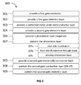
- FIG 2 schematically illustrates an example of a process flow in accordance with an embodiment of a method of the present disclosure.
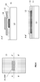
- FIG 3 to FIG 8 schematically illustrate process steps of an example of a method for fabricating a fully self-aligned dual-gate thin film transistor in accordance with an embodiment of the present disclosure.
- a schematic top view of the structure is shown at the left hand side and schematic cross sections along line A-A' and along line B-B' respectively are shown at the right hand side.
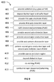
- FIG 9 schematically illustrates an example of a process flow for fabricating a fully self-aligned dual-gate thin film transistor in accordance with a method of the present disclosure.
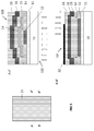
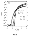
- FIG 10 shows I DS versus V GS transfer characteristics measured for a fully self-aligned dual-gate thin film transistor fabricated according to an embodiment of a method of the present disclosure (circles). As a reference, similar characteristics are shown for devices with back gate only (triangles) and for devices with top gate only (squares).
- FIG 11 shows I DS versus V DS output characteristics measured for a fully self-aligned dual-gate thin film transistor fabricated according to an embodiment of a method of the present disclosure (circles). As a reference, similar characteristics are shown for devices with back gate only (triangles) and for devices with top gate only (squares).
- 'self-aligned' means that a first element or feature of a device is aligned to a second element or feature of the device by performing a process wherein the second element or feature is used as a mask for defining the first element or feature. Alignment between two elements or features of the device is thus obtained by using one element or feature as a mask for patterning other elements or features.
- a metallic gate may be used as a mask for defining 'self-aligned' source and drain regions of the transistor.
- a first gate may be used as a mask for defining a 'self-aligned' second gate.
- 'fully self-aligned dual-gate thin film transistor (process)' refers to a dual-gate thin film transistor and corresponding fabrication process wherein the gates are self-aligned to each other and wherein the source and drain regions are self-aligned to a gate. More in particular, in the context of the present disclosure the bottom gate is used as a mask for defining (patterning) the top gate, and the top gate is used as a mask for defining the source and drain regions of the thin film transistor.
- FIG 1 schematically illustrates an example of a process flow in accordance with an embodiment of a method of the present disclosure.
- the method 200 shown in the process flow of FIG 1 comprises in a first step ( FIG 1 , step 201), providing a first gate electrode or bottom gate electrode on a substrate.
- Providing the first gate electrode or bottom gate electrode comprises depositing a bottom gate metallic layer and patterning the bottom gate metallic layer by means of photolithography to thereby form a first gate electrode or bottom gate electrode.
- the bottom gate electrode delimits, i.e. defines, a gate region.
- a first gate dielectric layer or bottom gate dielectric layer is provided, e.g. deposited, over the substrate and the first gate electrode.
- a patterned amorphous metal oxide semiconductor layer is provided ( FIG 1 , step 203) on the first gate dielectric layer.
- Providing the patterned amorphous metal oxide semiconductor layer comprises depositing an amorphous metal oxide semiconductor layer and patterning this layer by means of photolithography and dry or wet etching.
- the patterned metal oxide semiconductor layer delimits, i.e. defines, a semiconductor region.
- a second gate dielectric layer or top gate dielectric layer is provided over the metal oxide semiconductor layer and afterwards, at step 205 ( FIG 1 ), a second gate electrically conductive layer or top gate electrically conductive layer is provided on the second gate dielectric layer.
- a positive photoresist layer is provided ( FIG 1 , step 206) on the second gate electrically conductive layer and this photoresist layer is patterned ( FIG 1 , step 207). Patterning of the photoresist layer is done by performing a rear side illumination step ( FIG 1 , step 207a), a front side illumination step ( FIG 1 , step 207b) and a photoresist development step ( FIG 1 , step 207c), thereby forming a patterned photoresist layer.
- the rear side illumination step comprises illumination of the photoresist layer from a rear side of the substrate using the first gate electrode as a mask.
- the front side illumination step comprises illumination of the photoresist layer from the front side of the substrate using a mask exposing the photoresist layer in the gate region only in an edge part, the edge part being non-overlapping with the semiconductor region.
- the rear side illumination may be done first and afterwards the front side illumination may be done, or vice versa, first the front side illumination may be done and afterwards the rear side illumination.
- top gate electrically conductive layer or second gate electrically conductive layer is patterned ( FIG 1 , step 208) by locally etching the second gate electrically conductive layer using the patterned photoresist layer as a mask, thereby forming a second gate electrode.
- top gate dielectric layer or second gate dielectric layer is patterned ( FIG 1 , step 209) by locally etching the second gate dielectric layer using the patterned photoresist layer or the second gate electrode as a mask.
- FIG 2 schematically illustrates an example of a process flow in accordance with another embodiment of a method of the present disclosure.
- the method 300 shown in the process flow of FIG 2 comprises in a first step ( FIG 2 , step 301) providing a first gate electrode or bottom gate electrode on a substrate.
- Providing the first gate electrode or bottom gate electrode comprises depositing a bottom gate metallic layer and patterning the bottom gate metallic layer by means of photolithography to thereby form a first gate electrode or bottom gate electrode.
- the bottom gate electrode delimits, i.e. defines, a gate region.
- a first gate dielectric layer or bottom gate dielectric layer is provided, e.g. deposited, over the substrate and the first gate electrode.
- a patterned amorphous metal oxide semiconductor layer is provided ( FIG 2 , step 303) on the first gate dielectric layer.
- Providing the patterned amorphous metal oxide semiconductor layer comprises depositing an amorphous metal oxide semiconductor layer and patterning this layer by means of photolithography and dry or wet etching.
- the patterned metal oxide semiconductor layer delimits, i.e. defines, a semiconductor region.
- a second gate dielectric layer or top gate dielectric layer is provided over the metal oxide semiconductor layer.
- a negative photoresist layer is provided ( FIG 2 , step 306) and this photoresist layer is patterned ( FIG 2 , step 307).
- Patterning of the photoresist layer is done by performing a rear side illumination step ( FIG 2 , step 307a), a front side illumination step ( FIG 2 , step 307b) and a photoresist development step ( FIG 2 , step 307c), thereby forming a patterned photoresist layer.
- the rear side illumination step comprises illumination of the photoresist layer from a rear side of the substrate using the first gate electrode as a mask.
- the front side illumination step comprises illumination of the photoresist layer from the front side of the substrate using a mask exposing the photoresist layer in the gate region only in an edge part, the edge part being non-overlapping with the semiconductor region.
- the rear side illumination may be done first and afterwards the front side illumination may be done, or vice versa, first the front side illumination may be done and afterwards the rear side illumination.
- a second gate electrically conductive layer or top gate electrically conductive layer is provided ( FIG 2 , step 305).
- the top gate electrically conductive layer or second gate electrically conductive layer is patterned ( FIG 2 , step 308) by performing a lift-off process, thereby forming a second gate electrode.
- the top gate dielectric layer or second gate dielectric layer is patterned ( FIG 2 , step 309) by locally etching the second gate dielectric layer using the second gate electrode as a mask.
- FIG 3 to FIG 8 illustrate an example of a fabrication method of a fully self-aligned dual-gate thin film transistor 100 according to an embodiment of the present disclosure.
- a schematic top view of the fabricated structure is shown at the left hand side and schematic cross sections along line A-A' and along line B-B' respectively are shown at the right hand side.
- the top view is shown at a scale that is different from the scale of the cross sections.
- the corresponding process flow 400 is schematically illustrated in FIG 9 .
- the thin-film transistor is formed on a substrate 10, such as for example a glass substrate or a foil substrate.
- a substrate 10 such as for example a glass substrate or a foil substrate.
- the present disclosure is not limited thereto and other substrates may be used, provided they are substantially transparent to the wavelength used for the lithographic step defining the top gate electrode (using illumination through the substrate) as further described.
- a buffer layer and optionally a barrier layer are deposited ( FIG 9 , step 402) on a front side 101 of the substrate 10 as schematically illustrated in FIG 3 .
- the buffer layer and the barrier layer are shown as a single layer 11.
- a barrier layer is typically used in combination with a flexible substrate such as a foil substrate, but it may also be used in combination with other substrates such as glass substrates.
- the barrier layer and the buffer layer are dielectric layers.
- the barrier layer may for example be a silicon nitride layer or a polymer layer, e.g. having a thickness in the range between 100 nm and a 3 micrometer, the present disclosure not being limited thereto.
- the barrier layer protects the device from undesired influences from the substrate, e.g. from undesired diffusion of elements such as for example hydrogen from the substrate into the metal oxide semiconductor layer.
- the buffer layer may for example be a silicon oxide layer (e.g. deposited by PECVD (Plasma Enhanced Chemical Vapour Deposition)) or an aluminium oxide layer (e.g. deposited by ALD (Atomic Layer Deposition)).
- the buffer layer typically has a thickness in the range between 50 nm and 200 nm, but the present disclosure in not limited thereto.
- a buffer layer may for example be deposited for providing improved smoothness, i.e. for providing a surface with a better smoothness than the surface of the underlying layer (such as e.g. the buffer layer).
- Layer stacks comprising multiple barrier layers and/or multiple buffer layers may be used.
- a bottom gate (BG) metallic layer or first gate metallic layer is deposited and patterned by means of photolithography to thereby form a first gate electrode or bottom gate electrode 12 ( FIG 9 , step 403).
- the area or region corresponding to the location of the first gate electrode or bottom gate electrode 12, in other words the area or region delimited by the first gate electrode 12, is further referred to as the gate region 120 ( FIG 3 ).
- the bottom gate patterning step is the first photolithographic (PL) step, comprising providing a photoresist layer, illuminating the photoresist layer and developing the illuminated resist ( PL#1 ) .
- FIG 3 shows an example where the bottom gate electrode 12 has a rectangular shape with a wider portion at two opposite sides of the rectangle. This is only an example, and the present disclosure is not limited thereto. Other gate electrode shapes may be used.
- the bottom gate metallic layer i.e. the metallic layer for forming the first gate electrode or bottom gate electrode 12 may for example comprise Ti, Au, Mo, MoCr, TiN, Cu, W, AISi or TiW, the present disclosure not being limited thereto.
- the thickness may for example be in the range between 10 nm and 2 micrometer, the present disclosure not being limited thereto. It may for example be deposited by PVD (Physical Vapour Deposition), PECVD or evaporation, the present disclosure not being limited thereto. It may be a single layer or a layer stack comprising at least two layers.
- the thickness of the bottom gate dielectric layer 13 is typically in the range between 25 nm and 500 nm, the present disclosure not being limited thereto.
- an amorphous metal oxide semiconductor layer such as for example an amorphous IGZO layer is deposited ( FIG 9 , step 405), for example by PVD (such as e.g.
- this metal oxide semiconductor layer patterning step is the second photolithographic (PL) step, comprising providing a photoresist layer, illuminating the photoresist layer and developing the illuminated resist ( PL # 2 ).
- the amorphous metal oxide semiconductor layer 14 may for example comprise gallium-indium-zinc-oxide (GIZO or IGZO), or other metal oxide based semiconductors, e.g. of following compositions (without indication of the stoichiometry): ZnO, ZnSnO, InO, InZnO, InZnSnO, LaInZnO, GaInO, HfInZnO, MgZnO, LaInZnO, TiO, TiInSnO, TiInZnO, ScInZnO, SiInZnO and ZrInZnO, ZrZnSnO.
- GZO or IGZO gallium-indium-zinc-oxide
- the present disclosure is not limited thereto and the method in one aspect can be used with other suitable metal oxide semiconductors known to a person skilled in the art.
- These semiconductor layers can be provided by a multitude of methods such as for example sputtering, thermal evaporation, pulsed laser deposition, and spin-casting, ink-jet printing or drop casting of precursor solutions.
- the metal oxide semiconductor layer may have a thickness between 5 nm and 100 nm, for example between 10 nm and 50 nm, the present disclosure not being limited thereto.
- a second gate dielectric layer or top gate (TG) dielectric layer 15 such as for example a silicon oxide layer, an aluminium oxide layer or a hafnium oxide layer, is deposited ( FIG 9 , step 406), such as for example by means of PECVD, PVD, ALD or solution processing.
- the thickness of the second gate dielectric layer 15 is typically in the range between 25 nm and 500 nm, the present disclosure not being limited thereto.
- a second gate electrically conductive layer or top gate electrically conductive layer 16 is deposited ( FIG 9 , step 407), for forming a second gate electrode or top gate electrode of the thin film transistor 100.
- the top gate electrically conductive layer 16 is an electrically conductive layer that is substantially transparent to the wavelength used in the lithographic step for patterning the top gate electrically conductive layer 16 to thereby define a second gate electrode or top gate electrode (as described below).
- Examples of materials that may be used for forming the top gate electrically conductive layer 16 are ITO (Indium Tin Oxide), AZO (Aluminium doped Zinc Oxide) and TiN, the present disclosure not being limited thereto.
- the thickness of the top gate electrically conductive layer 16 is selected such that the layer is sufficiently transparent to the wavelength of the light used in the subsequent photolithographic step. For example, for an ITO layer 16 the thickness may be in the range between 10 nm and 100 nm.
- a TiN layer 16 the thickness is preferably not larger than 50 nm.
- a positive photoresist layer 21 is provided ( FIG 9 , step 408) on the top gate electrically conductive layer 16. This is schematically illustrated in FIG 5 .
- the photoresist layer 21 is patterned ( FIG 9 , step 408) by performing two illumination steps of the positive photoresist layer 21, as schematically illustrated in FIG 5 , followed by a step of developing the illuminated photoresist layer to thereby form a patterned photoresist layer.
- This patterning process comprises a rear side illumination step (as for example illustrated in FIG 1 , step 207a) and a front side illumination step (as for example illustrated in FIG 1 , step 207b).
- the structure shown in FIG 5 is illuminated from the rear side 102 of the substrate 10 (i.e. from the substrate side of the structure, i.e. the side opposite to the side where the layer stack and the photoresist layer 21 are provided) without using any dedicated mask.
- the bottom gate electrode 12 has the function of a mask for the illumination. It is an advantage of using the bottom gate electrode 12 as a mask that it allows forming a top gate electrode that is fully aligned with the bottom gate electrode.
- the structure is illuminated from the front side 101 using a mask 22 as illustrated in the cross section along line B-B' shown in FIG 5 .
- This mask 22 is designed such that in an area corresponding to the gate region 120, only an edge part (162, shown FIG 6 ) is exposed to the light during illumination through the mask.
- the edge part 162 is selected to be located such that within the gate region 120, it only overlaps with a part of a wider portion of the bottom gate.
- edge part 162 is only present in an area different from the area where the metal oxide semiconductor layer 14 is present.
- first the rear side illumination may be done and afterwards the front side illumination, or vice versa, first the front side illumination may be done and afterwards the rear side illumination.
- the photoresist layer 21 is developed to form a patterned photoresist layer.
- the top gate electrically conductive layer or second gate electrically conductive layer 16 and the top gate dielectric layer or second gate dielectric layer 15 are patterned ( FIG 9 , step 409) by dry or wet etching, using the remaining patterned photoresist layer as an etching mask.
- this top gate electrically conductive layer and top gate dielectric layer patterning step is the third photolithographic (PL) step, comprising providing a photoresist layer, illuminating the photoresist layer and developing the illuminated resist ( PL#3 ) .
- the resulting structure, showing the patterned top gate dielectric layer 151 and the top gate electrode or second gate electrode 161 (the patterned top gate electrically conductive layer 16) is schematically illustrated in FIG 6 .
- the top gate electrode 161 has the same shape as the bottom gate electrode 12, except for an edge part 162, where the top gate electrode 161 is not overlapping with the bottom gate electrode 12.
- FIG 9 step 410 a source region and a drain region are formed in the patterned metal oxide semiconductor layer 14.
- the source region and the drain region are self-aligned to the second gate electrode 161.
- Forming the source region and the drain region may for example comprise doping with hydrogen, implantation of dopants, plasma treatment or reduction of the metal oxide semiconductor material, using the second gate electrode as a mask.
- the step of forming a source region and a drain region may be combined with, e.g. it may be a result of, performing the next process step 411 ( FIG 9 ).
- a dielectric layer 17 is deposited ( FIG 9 , step 411) as illustrated in FIG 7 .
- the dielectric layer 17 may for example be a SiN x layer, e.g. having a thickness in the range between 50 nm and 500 nm. It may for example be deposited by PECVD.
- the dielectric layer 17 may advantageously be a SiN x layer because the deposition of such a layer may result in hydrogen doping of the exposed regions (i.e. in regions not covered by top gate electrode 161) of the amorphous metal oxide semiconductor layer 14, thereby forming a source region 141 and a drain region 142 in the metal oxide semiconductor layer 14, as schematically illustrated in FIG 7 .
- top gate electrode 161 is used as a mask for the doping step.
- vias 18 are defined by photolithography and dry or wet etching through the dielectric layer 17, for simultaneous contact opening to the source region 141, the drain region 142, the top gate electrode 161 and to the bottom gate electrode 12.
- this via formation step is the fourth photolithographic (PL) step, comprising providing a photoresist layer, illuminating the photoresist layer and developing the illuminated resist ( PL#4 ) . It is an advantage of a method according to embodiments of the present disclosure that there is no overlap between the top gate electrode 161 and the bottom gate electrode 12 in an area corresponding to the edge part 162.
- this allows to form openings or vias simultaneously, i.e. using a single patterning step, towards the source region 141, the drain region 142, the top gate electrode 161 and the bottom gate electrode 12. This allows saving one photolithographic step as compared to known methods for fabricating fully self-aligned dual-gate thin film transistors.
- an electrically conductive layer e.g. a metal layer or an electrically conductive oxide layer, is deposited and patterned by photolithography and etching (e.g. dry etching) to thereby form a source contact 191, a drain contact 192, a top gate contact or second gate contact 194 and a bottom gate contact or first gate contact 193 as illustrated in FIG 8 .
- the electrically conductive layer may for example contain Mo, MoCr, a Mo alloy, Al, W, Ti, TiN, Au or ITO, the present disclosure not being limited thereto.
- the thickness of this layer may for example be in the range between 50 nm and 500 nm, the present disclosure not being limited thereto.
- this contact or electrode formation step is the fifth photolithographic (PL) step, comprising providing a photoresist layer, illuminating the photoresist layer and developing the illuminated resist ( PL # 5 ).
- the samples may be annealed, for example at a temperature in the range between 150°C and 450°C, e.g. between 200°C and 300°C, for example in a N 2 , O 2 or air atmosphere for 1 to 12 hours.
- the process flow 400 schematically illustrated in FIG 9 is only an example of a method for fabricating a fully self-aligned dual-gate thin film transistor according to an embodiment of the present disclosure.
- the second gate electrically conductive layer may be provided after patterning the photoresist layer and patterning the second gate electrically conductive layer may comprise performing a lift-off process (as for example illustrated in FIG 2 ).
- Dual-gate thin film transistor devices 100 were fabricated in accordance with an embodiment of a method 400 ( FIG 9 ) of the present disclosure.
- a PECVD SiN x barrier layer was deposited, followed by Atomic Layer Deposition of a 100 nm thick Al 2 O 3 buffer layer at 150°C (step 402).
- step 402 Atomic Layer Deposition of a 100 nm thick Al 2 O 3 buffer layer at 150°C
- step 403 deposition of a 10 nm TiN / 50 nm AISi / 10 nm TiN layer stack and patterning of the stack using a sequence of dry and wet etching steps, to thereby form a first gate electrode or bottom gate electrode 12 (step 403).
- a first gate dielectric layer 13 consisting of 100 nm of Al 2 O 3 was deposited (step 404) at 150°C, followed by sputter deposition of a 24 nm thick amorphous IGZO layer (step 405).
- the amorphous IGZO layer was patterned using wet etching (step 405).
- a 100 nm thick silicon oxide second gate dielectric layer 15 was then deposited (step 406) by means of PECVD at 250°C, followed by deposition (step 407) of a 25 nm thick TiN second gate electrically conductive layer 16.
- the gate stack comprising the second gate electrically conductive layer 16 and the second gate dielectric layer 15 was patterned (step 409) by bottom and top exposures of a photoresist layer (step 408) according to a method of the present disclosure.
- the pattering (step 409) was done using a sequence of dry etching steps (CF 4 and SF 6 chemistry).
- a 400 nm thick SiN x dielectric layer 17 was deposited (step 411) at 150°C by means of PECVD.
- Contact opening step 412) was done using a sequence of dry and wet etching steps. This contact opening step was combined for both contacting the bottom gate electrode 12 and the top gate electrode 161, as well as the source region 141 and the drain region 142.
- a 10 nm Ti /80 nm AISi /10 nm Ti stack was deposited and patterned (step 413) using dry and wet etching steps, to thereby form a source contact 191, a drain contact 192, a bottom gate contact 193 and a top gate contact 194. Finally, the samples were annealed at 250°C in a N 2 atmosphere for 1 hour.
- the transistors had a W/L ratio of 15 micrometer /5 micrometer.
- similar characteristics are shown for the same device, but wherein during the measurement only the back gate is used (triangles) and wherein during the measurement only the top gate is used (squares) respectively.
- the dual-gate TFTs of the present disclosure show a steeper sub-threshold slope SS -1 and a higher on-current I ON when compared to single gate TFTs.
- the present disclosure also relates to a device obtained using a method according to any of the embodiments as described above.
Landscapes
- Thin Film Transistor (AREA)
Priority Applications (5)
| Application Number | Priority Date | Filing Date | Title |
|---|---|---|---|
| EP16165832.3A EP3236503A1 (fr) | 2016-04-18 | 2016-04-18 | Procédé de fabrication des transistors à couche mince à double grille complètement auto-alignée |
| TW106111299A TW201802892A (zh) | 2016-04-18 | 2017-03-31 | 完全自對準雙閘極薄膜電晶體的製造方法 |
| JP2017073455A JP2017208532A (ja) | 2016-04-18 | 2017-04-03 | 完全自己整合デュアルゲート薄膜トランジスタを製造するための方法 |
| KR1020170048395A KR20170119294A (ko) | 2016-04-18 | 2017-04-14 | 완전 자기-정렬된 듀얼-게이트 박막 트랜지스터를 제조하기 위한 방법 |
| CN201710252470.0A CN107305843A (zh) | 2016-04-18 | 2017-04-18 | 用于制造完全自对准双栅极薄膜晶体管的方法 |
Applications Claiming Priority (1)
| Application Number | Priority Date | Filing Date | Title |
|---|---|---|---|
| EP16165832.3A EP3236503A1 (fr) | 2016-04-18 | 2016-04-18 | Procédé de fabrication des transistors à couche mince à double grille complètement auto-alignée |
Publications (1)
| Publication Number | Publication Date |
|---|---|
| EP3236503A1 true EP3236503A1 (fr) | 2017-10-25 |
Family
ID=55759542
Family Applications (1)
| Application Number | Title | Priority Date | Filing Date |
|---|---|---|---|
| EP16165832.3A Withdrawn EP3236503A1 (fr) | 2016-04-18 | 2016-04-18 | Procédé de fabrication des transistors à couche mince à double grille complètement auto-alignée |
Country Status (5)
| Country | Link |
|---|---|
| EP (1) | EP3236503A1 (fr) |
| JP (1) | JP2017208532A (fr) |
| KR (1) | KR20170119294A (fr) |
| CN (1) | CN107305843A (fr) |
| TW (1) | TW201802892A (fr) |
Cited By (5)
| Publication number | Priority date | Publication date | Assignee | Title |
|---|---|---|---|---|
| GB2589937A (en) * | 2019-08-21 | 2021-06-16 | Pragmatic Printing Ltd | Electronic circuits and circuit elements |
| US11404543B2 (en) | 2020-06-19 | 2022-08-02 | Taiwan Semiconductor Manufacturing Company, Ltd. | Semiconductor device and manufacturing method thereof |
| US11462646B2 (en) | 2019-03-20 | 2022-10-04 | Ricoh Company, Ltd. | Field-effect transistor, display element, image display device, and system |
| US12159898B2 (en) | 2019-08-21 | 2024-12-03 | Pragmatic Semiconductor Limited | Resistor geometry |
| WO2025250330A1 (fr) * | 2024-05-31 | 2025-12-04 | Applied Materials, Inc. | Structures de transistor à couches minces |
Families Citing this family (3)
| Publication number | Priority date | Publication date | Assignee | Title |
|---|---|---|---|---|
| CN113261114A (zh) * | 2019-01-30 | 2021-08-13 | 深圳市柔宇科技股份有限公司 | 薄膜晶体管及其制作方法、显示面板及显示装置 |
| JP7293749B2 (ja) * | 2019-03-14 | 2023-06-20 | 富士電機株式会社 | 炭化珪素半導体装置の選別方法 |
| EP3767664B1 (fr) * | 2019-07-18 | 2024-08-28 | Imec VZW | Formation de motifs auto-alignés dans des couches |
Citations (2)
| Publication number | Priority date | Publication date | Assignee | Title |
|---|---|---|---|---|
| US7910419B2 (en) * | 2008-06-11 | 2011-03-22 | Commissariat A L'energie Atomique | SOI transistor with self-aligned ground plane and gate and buried oxide of variable thickness |
| US20130309808A1 (en) * | 2010-12-01 | 2013-11-21 | Peking University Shenzhen Graduate School | Method for manufacturing transistor |
-
2016
- 2016-04-18 EP EP16165832.3A patent/EP3236503A1/fr not_active Withdrawn
-
2017
- 2017-03-31 TW TW106111299A patent/TW201802892A/zh unknown
- 2017-04-03 JP JP2017073455A patent/JP2017208532A/ja not_active Withdrawn
- 2017-04-14 KR KR1020170048395A patent/KR20170119294A/ko not_active Withdrawn
- 2017-04-18 CN CN201710252470.0A patent/CN107305843A/zh not_active Withdrawn
Patent Citations (2)
| Publication number | Priority date | Publication date | Assignee | Title |
|---|---|---|---|---|
| US7910419B2 (en) * | 2008-06-11 | 2011-03-22 | Commissariat A L'energie Atomique | SOI transistor with self-aligned ground plane and gate and buried oxide of variable thickness |
| US20130309808A1 (en) * | 2010-12-01 | 2013-11-21 | Peking University Shenzhen Graduate School | Method for manufacturing transistor |
Non-Patent Citations (2)
| Title |
|---|
| XIN HE ET AL.: "Implementation of Fully Self-Aligned Homojunction Double-Gate a-IGZO TFTs", IEEE ELECTRON DEVICE LETTERS, vol. 35, no. 9, September 2014 (2014-09-01), pages 927 - 929, XP011557209 * |
| XIN HE ET AL.: "Implementation of Fully Self-Aligned Homojunction Double-Gate a-IGZO TFTs", IEEE ELECTRON DEVICE LETTERS, vol. 35, no. 9, September 2014 (2014-09-01), pages 927 - 929, XP011557209, DOI: doi:10.1109/LED.2014.2336232 |
Cited By (11)
| Publication number | Priority date | Publication date | Assignee | Title |
|---|---|---|---|---|
| US11462646B2 (en) | 2019-03-20 | 2022-10-04 | Ricoh Company, Ltd. | Field-effect transistor, display element, image display device, and system |
| GB2589937A (en) * | 2019-08-21 | 2021-06-16 | Pragmatic Printing Ltd | Electronic circuits and circuit elements |
| GB2589937B (en) * | 2019-08-21 | 2024-05-01 | Pragmatic Printing Ltd | Electronic circuits and circuit elements |
| US12159898B2 (en) | 2019-08-21 | 2024-12-03 | Pragmatic Semiconductor Limited | Resistor geometry |
| US12268014B2 (en) | 2019-08-21 | 2025-04-01 | Pragmatic Semiconductor Limited | Resistors for integrated circuits |
| US12342609B2 (en) | 2019-08-21 | 2025-06-24 | Pragmatic Semiconductor Limited | Electronic circuit comprising transistor and resistor |
| US12477754B2 (en) | 2019-08-21 | 2025-11-18 | Pragmatic Semiconductor Limited | Thin-film components for integrated circuits |
| US11404543B2 (en) | 2020-06-19 | 2022-08-02 | Taiwan Semiconductor Manufacturing Company, Ltd. | Semiconductor device and manufacturing method thereof |
| US11749723B2 (en) | 2020-06-19 | 2023-09-05 | Taiwan Semiconductor Manufacturing Company, Ltd. | Semiconductor device and manufacturing method thereof |
| US12034052B2 (en) | 2020-06-19 | 2024-07-09 | Taiwan Semiconductor Manufacturing Company, Ltd. | Semiconductor device and manufacturing method thereof |
| WO2025250330A1 (fr) * | 2024-05-31 | 2025-12-04 | Applied Materials, Inc. | Structures de transistor à couches minces |
Also Published As
| Publication number | Publication date |
|---|---|
| JP2017208532A (ja) | 2017-11-24 |
| CN107305843A (zh) | 2017-10-31 |
| TW201802892A (zh) | 2018-01-16 |
| KR20170119294A (ko) | 2017-10-26 |
Similar Documents
| Publication | Publication Date | Title |
|---|---|---|
| EP3236503A1 (fr) | Procédé de fabrication des transistors à couche mince à double grille complètement auto-alignée | |
| JP5775253B2 (ja) | 薄膜トランジスタ基板とその製造方法 | |
| EP2506308B1 (fr) | Procédé de fabrication d'un transistor à film mince d'oxyde amorphe | |
| US8101947B2 (en) | System and method for manufacturing a thin-film device | |
| US7863607B2 (en) | Thin film transistor array panel and manufacturing method thereof | |
| US10707236B2 (en) | Array substrate, manufacturing method therefor and display device | |
| US20170125452A1 (en) | Semiconductor device | |
| US20080203387A1 (en) | Thin film transistor and method of manufacturing the same | |
| US9048163B2 (en) | Transistor, electronic device including transistor, and manufacturing methods thereof | |
| JP2014131047A (ja) | 薄膜トランジスタ、および薄膜トランジスタ表示板 | |
| WO2016165186A1 (fr) | Procédé de fabrication d'un substrat de tft de semi-conducteur d'oxyde à double grille et structure de substrat de tft de semi-conducteur d'oxyde à double grille | |
| US8273600B2 (en) | Self-aligned metal oxide TFT with reduced number of masks | |
| WO2017219412A1 (fr) | Procédé de fabrication de transistor à couches minces de grille supérieure | |
| WO2016165185A1 (fr) | Procédé de fabrication d'un substrat de tft de semi-conducteur d'oxyde à double grille et structure de substrat de tft de semi-conducteur d'oxyde à double grille | |
| KR102586938B1 (ko) | 박막 트랜지스터 표시판 및 그 제조 방법 | |
| CN105006487A (zh) | 顶栅自对准金属氧化物半导体薄膜晶体管及制备方法 | |
| WO2017070868A1 (fr) | Procédé de fabrication de tft du type n | |
| WO2020244313A1 (fr) | Substrat matriciel et son procédé de préparation, panneau d'affichage et dispositif d'affichage | |
| US20160380105A1 (en) | Oxide thin film transistor and method for manufacturing the same, array substrate and method for manufacturing the same, and display device | |
| CN101533779A (zh) | 一种薄膜晶体管及图像显示装置的制作方法 | |
| CN114600234A (zh) | 电子电路和电路元件 | |
| CN107516661B (zh) | 显示基板、显示装置及显示基板的制作方法 | |
| JP2010205765A (ja) | 自己整合半導体トランジスタの製造方法 | |
| CN104576760A (zh) | 薄膜晶体管及其制备方法、阵列基板和显示装置 | |
| CN107946195B (zh) | 制备双栅氧化物半导体薄膜晶体管的方法 |
Legal Events
| Date | Code | Title | Description |
|---|---|---|---|
| PUAI | Public reference made under article 153(3) epc to a published international application that has entered the european phase |
Free format text: ORIGINAL CODE: 0009012 |
|
| AK | Designated contracting states |
Kind code of ref document: A1 Designated state(s): AL AT BE BG CH CY CZ DE DK EE ES FI FR GB GR HR HU IE IS IT LI LT LU LV MC MK MT NL NO PL PT RO RS SE SI SK SM TR |
|
| AX | Request for extension of the european patent |
Extension state: BA ME |
|
| 17P | Request for examination filed |
Effective date: 20180403 |
|
| RBV | Designated contracting states (corrected) |
Designated state(s): AL AT BE BG CH CY CZ DE DK EE ES FI FR GB GR HR HU IE IS IT LI LT LU LV MC MK MT NL NO PL PT RO RS SE SI SK SM TR |
|
| GRAP | Despatch of communication of intention to grant a patent |
Free format text: ORIGINAL CODE: EPIDOSNIGR1 |
|
| INTG | Intention to grant announced |
Effective date: 20200325 |
|
| STAA | Information on the status of an ep patent application or granted ep patent |
Free format text: STATUS: THE APPLICATION IS DEEMED TO BE WITHDRAWN |
|
| 18D | Application deemed to be withdrawn |
Effective date: 20200805 |