EP3236508A1 - Anzeigevorrichtung - Google Patents
Anzeigevorrichtung Download PDFInfo
- Publication number
- EP3236508A1 EP3236508A1 EP15870157.3A EP15870157A EP3236508A1 EP 3236508 A1 EP3236508 A1 EP 3236508A1 EP 15870157 A EP15870157 A EP 15870157A EP 3236508 A1 EP3236508 A1 EP 3236508A1
- Authority
- EP
- European Patent Office
- Prior art keywords
- mold
- coupling
- coupling portion
- display device
- module cover
- Prior art date
- Legal status (The legal status is an assumption and is not a legal conclusion. Google has not performed a legal analysis and makes no representation as to the accuracy of the status listed.)
- Granted
Links
Images









Classifications
-
- G—PHYSICS
- G06—COMPUTING OR CALCULATING; COUNTING
- G06F—ELECTRIC DIGITAL DATA PROCESSING
- G06F1/00—Details not covered by groups G06F3/00 - G06F13/00 and G06F21/00
- G06F1/16—Constructional details or arrangements
- G06F1/1601—Constructional details related to the housing of computer displays, e.g. of CRT monitors, of flat displays
-
- G—PHYSICS
- G09—EDUCATION; CRYPTOGRAPHY; DISPLAY; ADVERTISING; SEALS
- G09F—DISPLAYING; ADVERTISING; SIGNS; LABELS OR NAME-PLATES; SEALS
- G09F9/00—Indicating arrangements for variable information in which the information is built-up on a support by selection or combination of individual elements
- G09F9/30—Indicating arrangements for variable information in which the information is built-up on a support by selection or combination of individual elements in which the desired character or characters are formed by combining individual elements
- G09F9/33—Indicating arrangements for variable information in which the information is built-up on a support by selection or combination of individual elements in which the desired character or characters are formed by combining individual elements being semiconductor devices, e.g. diodes
-
- H—ELECTRICITY
- H05—ELECTRIC TECHNIQUES NOT OTHERWISE PROVIDED FOR
- H05K—PRINTED CIRCUITS; CASINGS OR CONSTRUCTIONAL DETAILS OF ELECTRIC APPARATUS; MANUFACTURE OF ASSEMBLAGES OF ELECTRICAL COMPONENTS
- H05K5/00—Casings, cabinets or drawers for electric apparatus
- H05K5/02—Details
- H05K5/03—Covers
-
- H—ELECTRICITY
- H10—SEMICONDUCTOR DEVICES; ELECTRIC SOLID-STATE DEVICES NOT OTHERWISE PROVIDED FOR
- H10K—ORGANIC ELECTRIC SOLID-STATE DEVICES
- H10K50/00—Organic light-emitting devices
- H10K50/80—Constructional details
- H10K50/84—Passivation; Containers; Encapsulations
-
- H—ELECTRICITY
- H10—SEMICONDUCTOR DEVICES; ELECTRIC SOLID-STATE DEVICES NOT OTHERWISE PROVIDED FOR
- H10K—ORGANIC ELECTRIC SOLID-STATE DEVICES
- H10K71/00—Manufacture or treatment specially adapted for the organic devices covered by this subclass
-
- G—PHYSICS
- G06—COMPUTING OR CALCULATING; COUNTING
- G06F—ELECTRIC DIGITAL DATA PROCESSING
- G06F2200/00—Indexing scheme relating to G06F1/04 - G06F1/32
- G06F2200/16—Indexing scheme relating to G06F1/16 - G06F1/18
- G06F2200/161—Indexing scheme relating to constructional details of the monitor
- G06F2200/1612—Flat panel monitor
Definitions
- the present invention relates to a display device of which rear cover capable of being slidably coupled easily.
- LCD liquid crystal display device
- PDP plasma display panel
- ELD electro luminescent display
- VFD vacuum fluorescent display
- a display device using an organic light emitting diode has an advantage of being excellent in luminance characteristics and viewing angle characteristics compared to a liquid crystal display device, and very thin owing to lack of a backlight unit.
- a display device comprising: a display panel; a module cover coupled with the display panel, the module cover positioned at a rear of the display panel; a rear cover slidably coupled to the module cover, the rear cover positioned at a rear of the module cover; a mold portion coupled with one of the module cover and the rear cover; and a coupling portion coupled with another of the module cover and the rear cover, the coupling portion corresponding to the mold portion.
- the mold portion may be slidably coupled to the coupling portion.
- the coupling portion may be located on at least one long edge of the module cover, and the coupling portion may include an opening open in a sliding direction of the rear cover.
- the coupling portion may include: a plurality of first coupling portions positioned at a periphery of the module cover, the plurality of first coupling portions placed spaced apart; and a plurality of second coupling portions positioned inner than the plurality of first coupling portions.
- the mold portion may comprise: a third coupling portion corresponding to the first coupling portion; and a fourth coupling portion corresponding to the second coupling portion, at least one of the first to fourth coupling portions may be elastically deformed, and a deformation of the third and fourth coupling portions may be greater than a deformation of the first and second coupling portions.
- the coupling portion may be located on at least one short edge of the module cover, and the coupling portion may include an opening open in a sliding direction of the rear cover.
- the coupling portion may include: a plurality of sixth coupling portions positioned at a periphery of the module cover, the plurality of sixth coupling portions placed spaced apart along to a direction of the sliding; a plurality of fifth coupling portions positioned inner than the plurality of sixth coupling portions; and a plurality of seventh coupling portions positioned inner than the plurality of sixth coupling portions, the plurality of seventh coupling portions placed alternatively with the plurality of the fifth coupling portions.
- the mold portion may comprise: a eighth coupling portion corresponding to the fifth coupling portion; a ninth coupling portion corresponding to the sixth coupling portion; and a tenth coupling portion corresponding to the seventh coupling portion
- the fifth coupling portion may be a mold
- the eighth coupling portion may be elastically deformed and contact with the fifth coupling portion
- the fifth coupling portion may include: a body portion; and a seating portion extended from the body portion, the eighth coupling portion may be seated at the seating portion of the fifth coupling portion, and a height of the body portion may be greater than a height of the seating portion.
- the display device may further comprise a plate positioned between the display panel and the module cover, and the plate may be coupled with at least one of the display panel and the module cover.
- the display panel may be an OLED (organic light emitting diodes) type.
- the rear cover is capable of being coupled slidably easily.
- first', 'second', etc. may be used to describe various components, but the components are not limited by such terms. The terms are used only for the purpose of distinguishing one component from other components.
- a first component may be designated as a second component without departing from the scope of the present invention.
- the second component may be designated as the first component.
- liquid crystal display panel as an example of a display panel.
- Other display panels may be used.
- a plasma display panel (PDP), a field emission display (FED) panel, and an organic light emitting diode (OLED) display panel may be used.
- a display device 100 may include a first long side LS1, a second long side LS2 opposite the first long side LS1, a first short side SS1 adjacent to the first long side LS1 and the second long side LS2, and a second short side SS2 opposite the first short side SS1.
- the embodiment of the invention describes that lengths of the first and second long sides LS1 and LS2 are longer than lengths of the first and second short sides SS1 and SS2 for the sake of brevity and ease of reading.
- the lengths of the first and second long sides LS1 and LS2 may be almost equal to the lengths of the first and second short sides SS1 and SS2.
- a first direction DR1 may be a direction parallel to the long sides LS1 and LS2 of the display device 100
- a second direction DR2 may be a direction parallel to the short sides SS1 and SS2 of the display device 100.
- a third direction DR3 may be a direction vertical to the first direction DR1 and/or the second direction DR2.
- first direction DR1 and the second direction DR2 may be commonly referred to as a horizontal direction.
- the third direction DR3 may be referred to as a vertical direction.
- the display device 100 may be of the OLED type. By using the display panel 110 which emits light by itself, the display device 100 may have relatively thin thickness.
- FIG. 2 is an exploded view of the display device of FIG. 1 .
- the display device 100 may include a display panel 110, a plate 120, a module cover 130, a rear cover 150, a bottom cover 140, and a mold portion 300.
- the bottom cover 140 may be coupled with a lower long side of the display device 100.
- the display panel 110 may display an image.
- the display panel 110 may include a plurality of layers.
- the display panel 100 may include a front substrate, a back substrate, and / or an optical layer.
- the display panel 110 may be an organic light emitting diode (OLED) panel that emits light by itself. In the case of an OLED panel, an auxiliary illumination for displaying an image may not be necessary.
- the display device 100 may be implemented with a relatively thin thickness, and may be capable of being curved.
- a plate 120 may be attached to a rear surface of the display panel 110.
- the plate 120 and the display panel 110 and / or the module cover 130 may be joined together by an adhesive tape.
- the display panel 110 may be attached to an front side of the plate 120, and the plate 120 may be attached to an front side of the module cover 130.
- the plate 120 and the display panel 110 and / or the module cover 130 may be coupled by a magnetic force.
- at least one of the plate 120, the display panel 110, and / or the module cover 130 may be magnetic and be attached to another. Disassembly / recombination of the plate 120, the display panel 110, and / or the module cover 130 may be facilitated in case of magnetic attachment.
- the plate 120 may be made of aluminum.
- the plate 120 may disperse heat transmitted to the display panel 110. Accordingly, heat concentration of the specific area of the display panel 110 is prevented, and deformation of the display panel 110 may be prevented.
- the module cover 130 may be attached to the plate 120.
- the module cover 130 and the plate 120 may be joined together by an adhesive tape or the like.
- the module cover 150 may be provided with a forming area.
- the forming region may serve to disperse and / or diffuse heat generated in an electronic circuit or the like.
- the rear cover 150 may be connected to the display panel 110 in a sliding manner in a direction from the first long side LS1 toward the second long side LS2, that is, in the second direction DR2. In other words, the rear cover 150 may be connected between the first short side SS1 of the display module 110 and the second short side SS2 against the first short side SS1.
- the rear cover 150 and / or other structures adjacent thereto may include protrusions, sliding portions, engaging portions, and the like.
- the mold portion 300 may be coupled to the rear cover 150 and / or the module cover 130.
- the mold portion 300 may be formed of a plastic material.
- the mold portion 300 may include first to third molds 310 to 330.
- the first mold 310 may be attached to the long side, and the second and third molds 330 and 350 may be attached to the short side.
- the mold portion 300 may be attached to the inner surface of the rear cover 150.
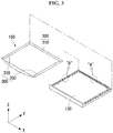
- FIGS. 3 to 13 are views showing the configuration of the display device of FIG. 2 .
- the display device 100 may easily and accurately slide and connect the rear cover 150 using the mold portion 300.
- the mold portion 300 may be attached to the rear cover 150.
- the first to third molds 310, 330, and 350 may be coupled to the inner edge of the rear cover 150.
- the module cover 130 may be provided with a configuration corresponding to the mold portion 300.
- a structure having a certain shape may be provided in a region adjacent to the upper long side of the module cover 130 and a region adjacent to the left and right short sides.
- the corresponding area of the module cover 130 may be press-processed.
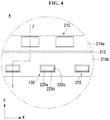
- FIG. 4 is a plan view of the module cover 130 at the A region.
- the first and second coupling portions 215 and 225 may be provided on the A region of the module cover 130 of the display device 100 according to an embodiment of the present invention.
- the first and second coupling portions 215 and 225 may be formed along the upper long side of the module cover 130.
- the first and second coupling portions 215 and 225 may be repeatedly formed along the edge area.
- the first and second coupling portions 215 and 225 may have an opening formed in the sliding direction of the rear cover 150.
- an opening may be formed to correspond to a direction from the upper side to the lower side of the display device 100, so that it can be combined with the structure inside the rear cover 150 to be slid.
- the first and second coupling portions 215 and 225 may be formed by pressing the corresponding region of the module cover 130.
- the first and second coupling portions 215 and 225 may be formed by pressing or removing a part of the plate-shaped module cover 130.
- the first coupling portion 215 may be formed in the first region 210a of the edge.
- the first region 210a may be a region that protrudes upward from the second region 210b.
- the height of the first and second regions 210a and 210b may be changed stepwise through the boundary area 212.
- the second coupling portion 225 may be formed in the second area 210b of the edge.
- the second coupling portion 225 may be located in the inner area than the first area 210a which is the outermost peripheral area.
- the second coupling portion 225 may include a body portion 225a, a boundary portion 225b, and a slit 225c.
- the first coupling portion 215 and the second coupling portion 225 may be arranged in a zigzag form. That is, the first coupling portion 215 and the second coupling portion 225 may be arranged so as not to overlap with each other in the Y direction.
- FIG. 5 is a cross-sectional view of the A region taken along the line I-I in the FIG. 4 .
- the first coupling portion 215 may have different height from that of the second coupling portion 212 due to the boundary area 212.
- the second coupling portion 225 may have a shape protruding in the Z direction as compared with the first coupling portion 215.
- the first coupling portion 215 may include an end portion 215a, a body portion 215b, and a groove portion 215c.
- the groove portion 215c may be an area in which a part of the body portion 215b is recessed inwardly. Due to the shape of the groove portion 215c, the counterpart coupled to the first coupling portion 215 may be securely coupled to the first coupling portion 215.
- the second coupling portion 225 may include an end portion 225d, a groove portion 224e, and a body 225f.
- the body 225f may extend from the module cover 130 via the boundary portion 225b.
- the second coupling portion 225 may protrude backward with respect to the first coupling portion 215.
- the second coupling portion 225 may be positioned on a plane different from a plane on which the first coupling portion 215.
- FIG. 6 and 7 are views showing a process of coupling the first and second coupling portions 215 and 225 with the first mold 310.
- the third and fourth coupling portions 315 and 325 of the first mold 310 may be slidably coupled with the first and second coupling portions 215 and 225.
- the third coupling portion 315 of the first mold 310 coupled to the upper long side inside the rear cover 150 may be coupled with the first coupling portion 215.
- the fourth coupling portion 325 may be coupled with the second coupling portion 225.
- the rear cover 150 may be slidably coupled with the module cover 130.
- the shapes of the first and second coupling portions 215 and 225 may correspond to the shapes of the third and fourth coupling portions 315 and 225.
- first and second coupling portions 215 and 225 at the module cover 130 and the third and fourth coupling portions 315 and 325 at the rear cover 150 may be coupled by being deformed within a certain extent.
- the body 225f of the second coupling portion 225 and the body 325f of the fourth coupling portion 325 corresponding thereto may be placed to form an overlapping area OL.
- the end portion 225d of the second coupling portion 225 may be in contact with the end portion 325a of the fourth coupling portion 325.
- the second coupling portion 225 and / or the fourth coupling portion 325 may be deformed.
- the second coupling portion 225 may be deformed in the first direction M1 and the fourth coupling portion 325 may be deformed in the second direction M2.
- the deformation in the second direction M2 occurs only.
- the deformation in the second direction M2 may be greater than that in the first direction M1.
- the second and fourth coupling portions 225 and 325 may be maintained in a state of being deformed to a certain extent.
- the coupling may be maintained in a state that the second and fourth coupling portions 225 and 325 are inclined with a horizontal axis.
- the second and fourth coupling portions 225 and 325 are in close contact with and coupled to each other due to the overlap region OL, which leads that the second and fourth coupling portions 225 and 325 can be firmly fastened. Noise and / or vibration due to the vibration of the second and fourth coupling portions 225, 325 can be prevented.
- FIG. 9 is a planar view of the module cover 130 in the B region shown in FIG. 3 .
- Fifth to seventh coupling portions 410, 420 and 430 may be formed in the B region of the module cover 130 of the display device 100 according to an embodiment of the present invention.
- the fifth to seventh coupling portions 410, 420, and 430 may have openings in the sliding direction of the rear cover 150.
- the fifth to seventh coupling portions 410, 420, and 430 may be repeatedly formed along the long side of the module cover 130.
- a first set S1 may include the fifth to seventh coupling portions 410, 420, 430.
- a second set S2 may include the fifth to seventh coupling portions 410, 420, 430.
- the second set S2 may be located beside the first set S1.
- the fifth to seventh coupling portions 410, 420 and 430 may be coupled with the mold portion 300 of the rear cover 150 when the rear cover 150 is coupled in sliding manner.
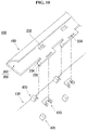
- FIG. 10 is a perspective view showing a coupling relationship between the module cover 130 and the rear cover 150.
- the rear cover 150 is expressed transparent or translucent.
- the mold portion 300 may be attached to the inside of the rear cover 150.
- a third mold 350 coupled to the long side may be located.
- the mold portion 300 may be provided with the eighth to tenth coupling portions 238, 232, and 234.
- the eighth to tenth coupling portions 238, 232 and 234 of the rear cover 150 may correspond to the fifth to seventh coupling portions 410, 420 and 430 of the module cover 130.
- the eighth to tenth coupling portions 238, 232, and 234 may be slidably coupled with the fifth to seventh coupling portions 410, 420, and 430.
- the eighth coupling portion 238 may be a slit formed in a part of the mold portion 300.
- the mold portion 300 may be in the form of penetrating.
- the eighth coupling portion 238 may correspond to the fifth coupling portion 410. The coupling relationship between the eighth coupling portion 238 and the fifth coupling portion 410 will be described later.
- the ninth coupling portion 232 may be a sliding coupling structure formed in a part of the mold portion 300.
- the ninth coupling portion 232 may be a latch which corresponds to the shape of the protruded sixth coupling portion 420.
- the tenth coupling portion 234 may be configured such that at least a part of the mold portion 300 protrudes to correspond to the seventh coupling portion 430.
- the tenth coupling portion 234 may be formed with an inclined portion 236 for smooth sliding engagement with the seventh coupling portion 430.
- the inclined portion 236 may be inclined in the Y and Z directions.
- the ninth and tenth engaging portions 232 and 234 may be located at flange portions protruding outward from the mold portion 300.
- the fifth and seventh engaging portions 410 and 430 may be located inside the sixth engaging portion 420 located at the outermost edge area of the module cover 130.
- the ninth and tenth engaging portions 232 and 234 may be located on a flange protruding in the X direction which is inner side in the body of the mold unit 300.
- FIG. 11 illustrates sliding engagement (coupling) of the mold portion 300.
- the mold portion 300 may be slid in the Y direction.
- the mold portion 300 may be in the first state.
- the eighth to tenth coupling portions 238, 232 and 234 of the mold portion 300 may be not coupled with the fifth to seventh coupling portions 410, 420 and 430 of the module cover 130.
- the eighth to tenth coupling portions 238, 232, and 234 may be inserted into the fifth to seventh coupling portions 410 420, and 430, respectively.
- FIG. 12 is a cross-sectional view taken along the line II-II of FIG. 11 (b) .
- the eighth to tenth coupling portions 238, 232, and 234 may be coupled with the fifth to seventh coupling portions 410, 420, and 430 in the second state.
- the ninth coupling portion 232 and the inclined portion 236 of the tenth coupling portion 234 can be inserted below the sixth and seventh coupling portions 420 and 430, respectively.
- the fifth coupling portion 410 may be a mold separately formed from the module cover 130.
- the fifth coupling portion 410 may be formed through a separate injection process and attached to the module cover 130.
- the eighth coupling portion 238 of the mold portion 300 may include a support bar 239.
- the support bar 239 may be pushed against the body portion 414 of the fifth coupling portion 410 to be coupled to the seating portion 412.
- the support bar 239 may be brought into close contact with the wall surface of the boundary between the body portion 414 and the seating portion 412.
- the width W1 of the central area of the eighth coupling portion 238 may be greater than the width W2 of the outer peripheral area of the eighth coupling portion 238.
- the support bar 239 may be coupled with the seating portion 412 of the fifth coupling portion 410.
- the seating portion 412 of the fifth coupling portion 410 may be formed lower than the body portion 414 of the fifth coupling portion 410.
- the height of the body portion 414 is H1
- the height of the seating portion 412 may be H2 smaller than H1.
- the support bar 239 may be coupled with the seating portion 412, while the support bar 239 is located higher than the lower surface of the contact portion 237. Due to such a positional relationship of the support bars 239, the support bar 239 can be more closely attached to the body portion 414 and the seating portion 412.
- FIG. 14 is an exploded view of a display device according to another embodiment of the present invention.
- a display device 100 may include a display panel 110, a plate 120, a module cover 130, a rear cover 150, and a mold portion 500.
- the mold portion 500 may be provided for sliding engagement (coupling) of the rear cover 150.
- the mold portion 500 may be integrally formed with at least one of the plate 120 and the module cover 130.
- the mold portion 500 may be extruded into at least one of the plate 120 and the module cover 130.
- the mold portion 500 may be made of a plastic material suitable for extrusion.
- the mold portion 500 may include first to third molds 520, 510, and 540.
- the first to third molds 520, 510, and 540 may be formed together or may be separately formed and assembled.
- FIG. 15 to 24 are views showing the configuration of the display device of FIG. 14 .
- the second mold 510 may include a mold guide 530.
- a plurality of mold guides 530 may be spaced apart at regular intervals along the Y direction of the second mold 510.
- the mold guide 530 may be made separately from the second mold 510 and be attached onto the second mold 510.
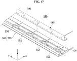
- FIG. 16 is a cross-sectional view showing the coupling relationship between the second mold 510 and the mold guide 530.
- the second mold 510 may have the engaging portion 152, the first and second fastening holes 154 and 156, and the rib 158.
- the engaging portion 152 may be a recessed region formed in a part of the second mold 510. An edge region of the rear cover 150 slidingly coupled to the second mold 510 may be inserted into the engaging portion 152.
- a first screw SC1 for coupling the mold guide 530 may be coupled with the first fastening hole 154.
- a second screw SC2 for coupling the module cover 130 with the second mold 510 may be coupled into the second fastening hole 156.
- the mold portion 500 according to an embodiment of the present invention may serve to fix the module cover 130. In case that the module cover 130 and the plate 120 are integrally formed, the mold portion 500 may serve to fix the module cover 130 and the plate 120 at a time.
- the rib 158 may be positioned between the first and second fastening holes 154 and 156.
- the rib 158 can serve as a guide in the process of coupling the mold guide 530 with the first coupling hole 154 and / or second coupling hole 156.
- the module cover 130 may smoothly be seated in the engagement position.
- the flange 145 of the rear cover 140 may be slidably coupled with the mold guide 530.
- the flange 145 inside the rear cover 140 may be coupled inside the respective mold guides 530.
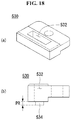
- the mold guide 530 may include a configuration for effective coupling with the rear cover 140.
- the mold guide 530 may include a depressed portion 532.
- the depressed portion 532 may be shaped such that a part of the body of the mold guide 530 is pushed forward.
- the depressed portion 532 may be concave with respect to the rear cover 150.
- the contact portion 534 may be located inside the depressed portion 532.
- the contact portion 534 may protrude forward as much as PR relative to the body of the mold guide 530. Since the contact portion 534 protrudes forward from the other portion of the mold guide 530, the contact portion 534 may be brought into close contact with the rear cover 140. Therefore, noise and / or vibration due to loose contact between the mold guide 530 and the rear cover 140 may be prevented.
- FIG. 19 is a cross-sectional view illustrating a state in which the rear cover 140 is coupled.
- the flange 145 bent inward of the rear cover 140 may be coupled between the mold guide 530 and the second mold 510.
- the contact portion 534 protruding from the mold guide 530 may press the flange 145. Therefore, the rear cover 140 may be firmly coupled and the rear cover 140 may be prevented from being shaken.
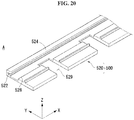
- FIG. 20 is a view showing "A" of the FIG. 15 .
- the first mold 520 may be provided with a cover insertion portion 522.
- the cover insertion portion 522 may be a depression formed in an end region of the first mold 520.
- the cover insertion portion 522 may be open toward other elements such as a support rib 528 or a slit 529.
- At least one support rib 528 may be formed in the first mold 520.
- the support ribs 528 may press the rear cover 150 coupled to the cover insertion portion 522 in the Z direction. Accordingly, it is possible to prevent the rear cover 150 from vibration and / or noise due to contact between the rear cover 150 and the first mold 520.
- slits 529 may be formed at regular intervals.
- the rear cover 140 may be slidably coupled with the first mold 520.
- the rear cover 140 may slide and be coupled in the Y direction.
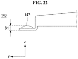
- an eleventh coupling portion 147 formed at the upper end of the rear cover 140 may be inserted into the cover insertion portion 522.
- the eleventh coupling portion 147 may be shaped to protrude in one direction.
- the eleventh coupling portion 147 may protrude backward as much as a distance BH from the rear cover 150.
- the eleventh coupling portion 147 may be brought into close contact with the first mold 520 within the cover insertion portion 522 due to the eleventh coupling portion 147.
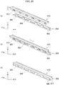
- the rear cover 150 may be slidingly coupled using a rail-shaped structure.
- the first rail 610 may be coupled to the inner side of the rear cover 150 and the second rail 630 may be coupled to the module cover 130.
- the second rail 610 may be formed on the mold portion 500.
- protrusions 612 may be formed on the first rails 610 at regular intervals.
- the size and spacing of the protrusions 612 may correspond to the spacing portion 634 formed on the side of the second rail 620.
- the spacing portion 634 may be a space between the neighboring sidewalls 632.
- the protrusion 612 may correspond to the groove 636 of the sidewall 632.
- the first rail 610 and the second rail 620 may be slid in the Y direction to be coupled.
- the protrusion 612 of the first rail 610 may be inserted into the sidewall 632 of the second rail 620 when the first rail 610 is slid.
- the first rail 610 and the second rail 630 may be coupled with each other.
- the first rail 610 may be coupled with the rear cover 140.
- the second rail 630 may be coupled with the module cover 130. Accordingly, due to the coupling of the first and second rails 610 and 630, the rear cover 140 and the module cover 130 may be coupled to each other.
Landscapes
- Engineering & Computer Science (AREA)
- Theoretical Computer Science (AREA)
- General Engineering & Computer Science (AREA)
- Physics & Mathematics (AREA)
- General Physics & Mathematics (AREA)
- Computer Hardware Design (AREA)
- Human Computer Interaction (AREA)
- Microelectronics & Electronic Packaging (AREA)
- Optics & Photonics (AREA)
- Manufacturing & Machinery (AREA)
- Devices For Indicating Variable Information By Combining Individual Elements (AREA)
- Electroluminescent Light Sources (AREA)
Applications Claiming Priority (3)
| Application Number | Priority Date | Filing Date | Title |
|---|---|---|---|
| KR1020140184972A KR102294764B1 (ko) | 2014-12-19 | 2014-12-19 | 디스플레이 장치 |
| KR1020140192694A KR20160080905A (ko) | 2014-12-29 | 2014-12-29 | 디스플레이 장치 |
| PCT/KR2015/008200 WO2016098989A1 (ko) | 2014-12-19 | 2015-08-05 | 디스플레이 장치 |
Publications (3)
| Publication Number | Publication Date |
|---|---|
| EP3236508A1 true EP3236508A1 (de) | 2017-10-25 |
| EP3236508A4 EP3236508A4 (de) | 2018-09-05 |
| EP3236508B1 EP3236508B1 (de) | 2022-04-13 |
Family
ID=56126838
Family Applications (1)
| Application Number | Title | Priority Date | Filing Date |
|---|---|---|---|
| EP15870157.3A Active EP3236508B1 (de) | 2014-12-19 | 2015-08-05 | Anzeigevorrichtung |
Country Status (4)
| Country | Link |
|---|---|
| US (1) | US10665814B2 (de) |
| EP (1) | EP3236508B1 (de) |
| CN (1) | CN107210015A (de) |
| WO (1) | WO2016098989A1 (de) |
Cited By (1)
| Publication number | Priority date | Publication date | Assignee | Title |
|---|---|---|---|---|
| EP3488604A4 (de) * | 2016-07-24 | 2020-03-18 | LG Electronics Inc. -1- | Anzeigevorrichtung |
Families Citing this family (7)
| Publication number | Priority date | Publication date | Assignee | Title |
|---|---|---|---|---|
| KR102639416B1 (ko) * | 2016-07-24 | 2024-02-22 | 엘지전자 주식회사 | 디스플레이 디바이스 |
| KR102557576B1 (ko) * | 2018-04-23 | 2023-07-24 | 엘지전자 주식회사 | 디스플레이 디바이스 |
| EP3561638B1 (de) | 2018-04-23 | 2021-03-10 | LG Electronics Inc. | Anzeigevorrichtung |
| CN109343260A (zh) * | 2018-11-28 | 2019-02-15 | 苏州佳世达电通有限公司 | 显示装置 |
| CN111290521B (zh) * | 2018-12-06 | 2022-10-28 | 鸿富锦精密工业(武汉)有限公司 | 触控模块化显示装置 |
| JP7074111B2 (ja) * | 2019-06-27 | 2022-05-24 | 株式会社Jvcケンウッド | 表示装置、電子機器及び組み付け方法 |
| CN111047978A (zh) * | 2020-01-13 | 2020-04-21 | 陈晓锋 | 一种电子信息用大屏幕显示屏 |
Family Cites Families (28)
| Publication number | Priority date | Publication date | Assignee | Title |
|---|---|---|---|---|
| JP2002290873A (ja) * | 2001-03-26 | 2002-10-04 | Nec Corp | 表示パネルの支持枠製造方法、表示パネルの支持枠及び表示装置 |
| JP4466013B2 (ja) | 2003-08-27 | 2010-05-26 | ソニー株式会社 | パネル型表示装置 |
| JP3110945U (ja) * | 2005-03-02 | 2005-07-07 | 船井電機株式会社 | 液晶表示装置 |
| JP5061277B2 (ja) * | 2005-11-21 | 2012-10-31 | 株式会社ジャパンディスプレイイースト | 表示装置 |
| KR20080022721A (ko) * | 2006-09-07 | 2008-03-12 | 삼성전자주식회사 | 표시장치용 커버 및 이를 갖는 표시장치 |
| KR101338023B1 (ko) * | 2006-12-04 | 2013-12-06 | 삼성디스플레이 주식회사 | 표시 장치 |
| JP2008158432A (ja) * | 2006-12-26 | 2008-07-10 | Hitachi Displays Ltd | 液晶表示装置 |
| WO2009002103A2 (en) * | 2007-06-26 | 2008-12-31 | Mtx Hybrid Co., Ltd. | Sliding module and sliding device having the same |
| KR20080114449A (ko) * | 2007-06-26 | 2008-12-31 | 주식회사 엠티엑스하이브리드 | 슬라이딩 모듈 및 이를 포함하는 슬라이딩 장치 |
| KR20100113196A (ko) * | 2009-04-13 | 2010-10-21 | 엘지전자 주식회사 | 디스플레이 장치 |
| CN101625815A (zh) * | 2009-08-04 | 2010-01-13 | 幸琳 | 一种用于led显示屏的安装装置和led显示屏 |
| KR101571170B1 (ko) * | 2009-08-20 | 2015-11-23 | 엘지전자 주식회사 | 디스플레이 장치 |
| KR20110019501A (ko) * | 2009-08-20 | 2011-02-28 | 엘지전자 주식회사 | 디스플레이 장치 |
| WO2011125628A1 (ja) * | 2010-04-01 | 2011-10-13 | シャープ株式会社 | 表示装置 |
| WO2012120739A1 (ja) * | 2011-03-04 | 2012-09-13 | パナソニック株式会社 | 照明装置 |
| CN102867461B (zh) * | 2011-07-05 | 2015-03-11 | 乐金显示有限公司 | 平板型图像显示装置及其制造方法 |
| US8953115B2 (en) * | 2011-11-18 | 2015-02-10 | Shenzhen China Star Optoelectronics Technology Co., Ltd. | Flat panel display device, stereoscopic display device, and plasma display device |
| CN102402061A (zh) * | 2011-11-18 | 2012-04-04 | 深圳市华星光电技术有限公司 | 液晶模块拼接式背板及其拼接构造 |
| US8757861B2 (en) * | 2012-01-27 | 2014-06-24 | Samsung Display Co., Ltd. | Flat panel display device and method for manufacturing the same |
| CN202841761U (zh) * | 2012-09-04 | 2013-03-27 | 深圳市奥拓电子股份有限公司 | 一种led显示模组及其快速拆装装置 |
| CN103177665A (zh) * | 2013-04-08 | 2013-06-26 | 深圳市雷迪奥光电技术有限公司 | 一种led显示屏 |
| KR102175948B1 (ko) * | 2013-06-05 | 2020-11-09 | 삼성디스플레이 주식회사 | 표시장치 |
| KR102068798B1 (ko) * | 2013-06-26 | 2020-01-22 | 엘지전자 주식회사 | 영상표시기기 |
| CN103413501B (zh) * | 2013-08-19 | 2015-09-09 | 深圳市通普科技有限公司 | 安装模组及含有该安装模组的led显示组件 |
| US9655258B2 (en) * | 2014-05-30 | 2017-05-16 | Lg Electronics Inc. | Display device |
| KR102269968B1 (ko) * | 2014-12-08 | 2021-06-28 | 엘지전자 주식회사 | 디스플레이 장치 |
| KR20160024049A (ko) * | 2014-08-22 | 2016-03-04 | 삼성디스플레이 주식회사 | 표시 장치 |
| KR20170119361A (ko) * | 2016-04-18 | 2017-10-27 | 삼성디스플레이 주식회사 | 표시 장치 |
-
2015
- 2015-08-05 WO PCT/KR2015/008200 patent/WO2016098989A1/ko not_active Ceased
- 2015-08-05 CN CN201580068819.4A patent/CN107210015A/zh active Pending
- 2015-08-05 EP EP15870157.3A patent/EP3236508B1/de active Active
- 2015-08-05 US US15/537,856 patent/US10665814B2/en active Active
Cited By (1)
| Publication number | Priority date | Publication date | Assignee | Title |
|---|---|---|---|---|
| EP3488604A4 (de) * | 2016-07-24 | 2020-03-18 | LG Electronics Inc. -1- | Anzeigevorrichtung |
Also Published As
| Publication number | Publication date |
|---|---|
| WO2016098989A1 (ko) | 2016-06-23 |
| US10665814B2 (en) | 2020-05-26 |
| US20170352831A1 (en) | 2017-12-07 |
| CN107210015A (zh) | 2017-09-26 |
| EP3236508B1 (de) | 2022-04-13 |
| EP3236508A4 (de) | 2018-09-05 |
Similar Documents
| Publication | Publication Date | Title |
|---|---|---|
| EP3236508B1 (de) | Anzeigevorrichtung | |
| US10194542B2 (en) | Display device having display panel and a case that covers an edge of the display panel | |
| US9766488B2 (en) | Liquid crystal display apparatus and display apparatus | |
| KR102294764B1 (ko) | 디스플레이 장치 | |
| JP5536833B2 (ja) | 表示装置及びテレビジョン受信機 | |
| CN111336167B (zh) | 显示模块紧固组件以及包括其的多显示器装置 | |
| US9025104B2 (en) | Backboard structure, backlight module, liquid crystal display module | |
| US9519169B2 (en) | Liquid crystal display device, configurational structure of front frame and middle frame thereof | |
| US20110317415A1 (en) | Electronic device | |
| KR101488235B1 (ko) | 백라이트 장치의 광학시트 고정 구조 | |
| EP2081076A2 (de) | Flüssigkristallanzeigetafel | |
| EP2977814A1 (de) | Anzeigevorrichtung | |
| US9588364B2 (en) | Display device | |
| US9739930B2 (en) | Backlight module having a frame element, light bar, light guiding plate and light bar cover | |
| US20150370132A1 (en) | Backplate Assembly, Backlight Module and Display Device | |
| US20170261802A1 (en) | Backlight Module And Display Device | |
| US9734736B2 (en) | Electronic device having self-emitting display panel | |
| KR20160080905A (ko) | 디스플레이 장치 | |
| EP3264400B1 (de) | Rückplatte für verwendung in einer anzeigevorrichtung und anzeigevorrichtung mit einer solchen rückplatte | |
| WO2014057717A1 (en) | Television and electronic apparatus | |
| CN102298222A (zh) | 显示装置及其组合方法以及两个框体的组合结构及其组合方法 | |
| US10838242B2 (en) | Display device with protection plate having larger rear surface area than front surface of front substrate area | |
| JP6557508B2 (ja) | 表示装置及びテレビジョン受信機 | |
| CN1963622A (zh) | 背光模组 | |
| US20130127830A1 (en) | Flat Panel Display Device and Stereoscopic Display Device |
Legal Events
| Date | Code | Title | Description |
|---|---|---|---|
| STAA | Information on the status of an ep patent application or granted ep patent |
Free format text: STATUS: THE INTERNATIONAL PUBLICATION HAS BEEN MADE |
|
| PUAI | Public reference made under article 153(3) epc to a published international application that has entered the european phase |
Free format text: ORIGINAL CODE: 0009012 |
|
| STAA | Information on the status of an ep patent application or granted ep patent |
Free format text: STATUS: REQUEST FOR EXAMINATION WAS MADE |
|
| 17P | Request for examination filed |
Effective date: 20170718 |
|
| AK | Designated contracting states |
Kind code of ref document: A1 Designated state(s): AL AT BE BG CH CY CZ DE DK EE ES FI FR GB GR HR HU IE IS IT LI LT LU LV MC MK MT NL NO PL PT RO RS SE SI SK SM TR |
|
| AX | Request for extension of the european patent |
Extension state: BA ME |
|
| DAV | Request for validation of the european patent (deleted) | ||
| DAX | Request for extension of the european patent (deleted) | ||
| RIC1 | Information provided on ipc code assigned before grant |
Ipc: G06F 1/16 20060101AFI20180726BHEP |
|
| A4 | Supplementary search report drawn up and despatched |
Effective date: 20180803 |
|
| STAA | Information on the status of an ep patent application or granted ep patent |
Free format text: STATUS: EXAMINATION IS IN PROGRESS |
|
| 17Q | First examination report despatched |
Effective date: 20200514 |
|
| REG | Reference to a national code |
Ref country code: DE Ref legal event code: R079 Ref document number: 602015078267 Country of ref document: DE Free format text: PREVIOUS MAIN CLASS: H01L0051560000 Ipc: G06F0001160000 |
|
| GRAP | Despatch of communication of intention to grant a patent |
Free format text: ORIGINAL CODE: EPIDOSNIGR1 |
|
| STAA | Information on the status of an ep patent application or granted ep patent |
Free format text: STATUS: GRANT OF PATENT IS INTENDED |
|
| RIC1 | Information provided on ipc code assigned before grant |
Ipc: G06F 1/16 20060101AFI20211122BHEP |
|
| INTG | Intention to grant announced |
Effective date: 20211222 |
|
| GRAS | Grant fee paid |
Free format text: ORIGINAL CODE: EPIDOSNIGR3 |
|
| GRAA | (expected) grant |
Free format text: ORIGINAL CODE: 0009210 |
|
| STAA | Information on the status of an ep patent application or granted ep patent |
Free format text: STATUS: THE PATENT HAS BEEN GRANTED |
|
| AK | Designated contracting states |
Kind code of ref document: B1 Designated state(s): AL AT BE BG CH CY CZ DE DK EE ES FI FR GB GR HR HU IE IS IT LI LT LU LV MC MK MT NL NO PL PT RO RS SE SI SK SM TR |
|
| REG | Reference to a national code |
Ref country code: GB Ref legal event code: FG4D |
|
| REG | Reference to a national code |
Ref country code: CH Ref legal event code: EP |
|
| REG | Reference to a national code |
Ref country code: DE Ref legal event code: R096 Ref document number: 602015078267 Country of ref document: DE |
|
| REG | Reference to a national code |
Ref country code: IE Ref legal event code: FG4D |
|
| REG | Reference to a national code |
Ref country code: AT Ref legal event code: REF Ref document number: 1483902 Country of ref document: AT Kind code of ref document: T Effective date: 20220515 |
|
| REG | Reference to a national code |
Ref country code: LT Ref legal event code: MG9D |
|
| REG | Reference to a national code |
Ref country code: NL Ref legal event code: MP Effective date: 20220413 |
|
| REG | Reference to a national code |
Ref country code: AT Ref legal event code: MK05 Ref document number: 1483902 Country of ref document: AT Kind code of ref document: T Effective date: 20220413 |
|
| PG25 | Lapsed in a contracting state [announced via postgrant information from national office to epo] |
Ref country code: NL Free format text: LAPSE BECAUSE OF FAILURE TO SUBMIT A TRANSLATION OF THE DESCRIPTION OR TO PAY THE FEE WITHIN THE PRESCRIBED TIME-LIMIT Effective date: 20220413 |
|
| PG25 | Lapsed in a contracting state [announced via postgrant information from national office to epo] |
Ref country code: SE Free format text: LAPSE BECAUSE OF FAILURE TO SUBMIT A TRANSLATION OF THE DESCRIPTION OR TO PAY THE FEE WITHIN THE PRESCRIBED TIME-LIMIT Effective date: 20220413 Ref country code: PT Free format text: LAPSE BECAUSE OF FAILURE TO SUBMIT A TRANSLATION OF THE DESCRIPTION OR TO PAY THE FEE WITHIN THE PRESCRIBED TIME-LIMIT Effective date: 20220816 Ref country code: NO Free format text: LAPSE BECAUSE OF FAILURE TO SUBMIT A TRANSLATION OF THE DESCRIPTION OR TO PAY THE FEE WITHIN THE PRESCRIBED TIME-LIMIT Effective date: 20220713 Ref country code: LT Free format text: LAPSE BECAUSE OF FAILURE TO SUBMIT A TRANSLATION OF THE DESCRIPTION OR TO PAY THE FEE WITHIN THE PRESCRIBED TIME-LIMIT Effective date: 20220413 Ref country code: HR Free format text: LAPSE BECAUSE OF FAILURE TO SUBMIT A TRANSLATION OF THE DESCRIPTION OR TO PAY THE FEE WITHIN THE PRESCRIBED TIME-LIMIT Effective date: 20220413 Ref country code: GR Free format text: LAPSE BECAUSE OF FAILURE TO SUBMIT A TRANSLATION OF THE DESCRIPTION OR TO PAY THE FEE WITHIN THE PRESCRIBED TIME-LIMIT Effective date: 20220714 Ref country code: FI Free format text: LAPSE BECAUSE OF FAILURE TO SUBMIT A TRANSLATION OF THE DESCRIPTION OR TO PAY THE FEE WITHIN THE PRESCRIBED TIME-LIMIT Effective date: 20220413 Ref country code: ES Free format text: LAPSE BECAUSE OF FAILURE TO SUBMIT A TRANSLATION OF THE DESCRIPTION OR TO PAY THE FEE WITHIN THE PRESCRIBED TIME-LIMIT Effective date: 20220413 Ref country code: BG Free format text: LAPSE BECAUSE OF FAILURE TO SUBMIT A TRANSLATION OF THE DESCRIPTION OR TO PAY THE FEE WITHIN THE PRESCRIBED TIME-LIMIT Effective date: 20220713 Ref country code: AT Free format text: LAPSE BECAUSE OF FAILURE TO SUBMIT A TRANSLATION OF THE DESCRIPTION OR TO PAY THE FEE WITHIN THE PRESCRIBED TIME-LIMIT Effective date: 20220413 |
|
| PG25 | Lapsed in a contracting state [announced via postgrant information from national office to epo] |
Ref country code: RS Free format text: LAPSE BECAUSE OF FAILURE TO SUBMIT A TRANSLATION OF THE DESCRIPTION OR TO PAY THE FEE WITHIN THE PRESCRIBED TIME-LIMIT Effective date: 20220413 Ref country code: PL Free format text: LAPSE BECAUSE OF FAILURE TO SUBMIT A TRANSLATION OF THE DESCRIPTION OR TO PAY THE FEE WITHIN THE PRESCRIBED TIME-LIMIT Effective date: 20220413 Ref country code: LV Free format text: LAPSE BECAUSE OF FAILURE TO SUBMIT A TRANSLATION OF THE DESCRIPTION OR TO PAY THE FEE WITHIN THE PRESCRIBED TIME-LIMIT Effective date: 20220413 Ref country code: IS Free format text: LAPSE BECAUSE OF FAILURE TO SUBMIT A TRANSLATION OF THE DESCRIPTION OR TO PAY THE FEE WITHIN THE PRESCRIBED TIME-LIMIT Effective date: 20220813 |
|
| REG | Reference to a national code |
Ref country code: DE Ref legal event code: R097 Ref document number: 602015078267 Country of ref document: DE |
|
| PG25 | Lapsed in a contracting state [announced via postgrant information from national office to epo] |
Ref country code: SM Free format text: LAPSE BECAUSE OF FAILURE TO SUBMIT A TRANSLATION OF THE DESCRIPTION OR TO PAY THE FEE WITHIN THE PRESCRIBED TIME-LIMIT Effective date: 20220413 Ref country code: SK Free format text: LAPSE BECAUSE OF FAILURE TO SUBMIT A TRANSLATION OF THE DESCRIPTION OR TO PAY THE FEE WITHIN THE PRESCRIBED TIME-LIMIT Effective date: 20220413 Ref country code: RO Free format text: LAPSE BECAUSE OF FAILURE TO SUBMIT A TRANSLATION OF THE DESCRIPTION OR TO PAY THE FEE WITHIN THE PRESCRIBED TIME-LIMIT Effective date: 20220413 Ref country code: EE Free format text: LAPSE BECAUSE OF FAILURE TO SUBMIT A TRANSLATION OF THE DESCRIPTION OR TO PAY THE FEE WITHIN THE PRESCRIBED TIME-LIMIT Effective date: 20220413 Ref country code: DK Free format text: LAPSE BECAUSE OF FAILURE TO SUBMIT A TRANSLATION OF THE DESCRIPTION OR TO PAY THE FEE WITHIN THE PRESCRIBED TIME-LIMIT Effective date: 20220413 Ref country code: CZ Free format text: LAPSE BECAUSE OF FAILURE TO SUBMIT A TRANSLATION OF THE DESCRIPTION OR TO PAY THE FEE WITHIN THE PRESCRIBED TIME-LIMIT Effective date: 20220413 |
|
| PLBE | No opposition filed within time limit |
Free format text: ORIGINAL CODE: 0009261 |
|
| STAA | Information on the status of an ep patent application or granted ep patent |
Free format text: STATUS: NO OPPOSITION FILED WITHIN TIME LIMIT |
|
| 26N | No opposition filed |
Effective date: 20230116 |
|
| PG25 | Lapsed in a contracting state [announced via postgrant information from national office to epo] |
Ref country code: MC Free format text: LAPSE BECAUSE OF FAILURE TO SUBMIT A TRANSLATION OF THE DESCRIPTION OR TO PAY THE FEE WITHIN THE PRESCRIBED TIME-LIMIT Effective date: 20220413 Ref country code: AL Free format text: LAPSE BECAUSE OF FAILURE TO SUBMIT A TRANSLATION OF THE DESCRIPTION OR TO PAY THE FEE WITHIN THE PRESCRIBED TIME-LIMIT Effective date: 20220413 |
|
| REG | Reference to a national code |
Ref country code: CH Ref legal event code: PL |
|
| PG25 | Lapsed in a contracting state [announced via postgrant information from national office to epo] |
Ref country code: LU Free format text: LAPSE BECAUSE OF NON-PAYMENT OF DUE FEES Effective date: 20220805 Ref country code: LI Free format text: LAPSE BECAUSE OF NON-PAYMENT OF DUE FEES Effective date: 20220831 Ref country code: CH Free format text: LAPSE BECAUSE OF NON-PAYMENT OF DUE FEES Effective date: 20220831 |
|
| REG | Reference to a national code |
Ref country code: BE Ref legal event code: MM Effective date: 20220831 |
|
| PG25 | Lapsed in a contracting state [announced via postgrant information from national office to epo] |
Ref country code: SI Free format text: LAPSE BECAUSE OF FAILURE TO SUBMIT A TRANSLATION OF THE DESCRIPTION OR TO PAY THE FEE WITHIN THE PRESCRIBED TIME-LIMIT Effective date: 20220413 |
|
| PG25 | Lapsed in a contracting state [announced via postgrant information from national office to epo] |
Ref country code: IE Free format text: LAPSE BECAUSE OF NON-PAYMENT OF DUE FEES Effective date: 20220805 |
|
| PG25 | Lapsed in a contracting state [announced via postgrant information from national office to epo] |
Ref country code: BE Free format text: LAPSE BECAUSE OF NON-PAYMENT OF DUE FEES Effective date: 20220831 |
|
| REG | Reference to a national code |
Ref country code: DE Ref legal event code: R082 Ref document number: 602015078267 Country of ref document: DE Representative=s name: TER MEER STEINMEISTER & PARTNER PATENTANWAELTE, DE |
|
| PG25 | Lapsed in a contracting state [announced via postgrant information from national office to epo] |
Ref country code: IT Free format text: LAPSE BECAUSE OF FAILURE TO SUBMIT A TRANSLATION OF THE DESCRIPTION OR TO PAY THE FEE WITHIN THE PRESCRIBED TIME-LIMIT Effective date: 20220413 |
|
| PG25 | Lapsed in a contracting state [announced via postgrant information from national office to epo] |
Ref country code: HU Free format text: LAPSE BECAUSE OF FAILURE TO SUBMIT A TRANSLATION OF THE DESCRIPTION OR TO PAY THE FEE WITHIN THE PRESCRIBED TIME-LIMIT; INVALID AB INITIO Effective date: 20150805 |
|
| PG25 | Lapsed in a contracting state [announced via postgrant information from national office to epo] |
Ref country code: CY Free format text: LAPSE BECAUSE OF FAILURE TO SUBMIT A TRANSLATION OF THE DESCRIPTION OR TO PAY THE FEE WITHIN THE PRESCRIBED TIME-LIMIT Effective date: 20220413 |
|
| PG25 | Lapsed in a contracting state [announced via postgrant information from national office to epo] |
Ref country code: MK Free format text: LAPSE BECAUSE OF FAILURE TO SUBMIT A TRANSLATION OF THE DESCRIPTION OR TO PAY THE FEE WITHIN THE PRESCRIBED TIME-LIMIT Effective date: 20220413 |
|
| PG25 | Lapsed in a contracting state [announced via postgrant information from national office to epo] |
Ref country code: MT Free format text: LAPSE BECAUSE OF FAILURE TO SUBMIT A TRANSLATION OF THE DESCRIPTION OR TO PAY THE FEE WITHIN THE PRESCRIBED TIME-LIMIT Effective date: 20220413 |
|
| PG25 | Lapsed in a contracting state [announced via postgrant information from national office to epo] |
Ref country code: BG Free format text: LAPSE BECAUSE OF FAILURE TO SUBMIT A TRANSLATION OF THE DESCRIPTION OR TO PAY THE FEE WITHIN THE PRESCRIBED TIME-LIMIT Effective date: 20220413 |
|
| PG25 | Lapsed in a contracting state [announced via postgrant information from national office to epo] |
Ref country code: BG Free format text: LAPSE BECAUSE OF FAILURE TO SUBMIT A TRANSLATION OF THE DESCRIPTION OR TO PAY THE FEE WITHIN THE PRESCRIBED TIME-LIMIT Effective date: 20220413 |
|
| PGFP | Annual fee paid to national office [announced via postgrant information from national office to epo] |
Ref country code: DE Payment date: 20250707 Year of fee payment: 11 |
|
| PGFP | Annual fee paid to national office [announced via postgrant information from national office to epo] |
Ref country code: GB Payment date: 20250707 Year of fee payment: 11 |
|
| PGFP | Annual fee paid to national office [announced via postgrant information from national office to epo] |
Ref country code: FR Payment date: 20250715 Year of fee payment: 11 |
|
| PG25 | Lapsed in a contracting state [announced via postgrant information from national office to epo] |
Ref country code: TR Free format text: LAPSE BECAUSE OF FAILURE TO SUBMIT A TRANSLATION OF THE DESCRIPTION OR TO PAY THE FEE WITHIN THE PRESCRIBED TIME-LIMIT Effective date: 20220413 |