EP3236647A1 - Capteur d'image, et procédé de sortie, procédé de focalisation de phase, appareil d'imagerie, et terminal - Google Patents
Capteur d'image, et procédé de sortie, procédé de focalisation de phase, appareil d'imagerie, et terminal Download PDFInfo
- Publication number
- EP3236647A1 EP3236647A1 EP16874631.1A EP16874631A EP3236647A1 EP 3236647 A1 EP3236647 A1 EP 3236647A1 EP 16874631 A EP16874631 A EP 16874631A EP 3236647 A1 EP3236647 A1 EP 3236647A1
- Authority
- EP
- European Patent Office
- Prior art keywords
- photosensitive unit
- photosensitive
- array
- pixels
- image sensor
- Prior art date
- Legal status (The legal status is an assumption and is not a legal conclusion. Google has not performed a legal analysis and makes no representation as to the accuracy of the status listed.)
- Ceased
Links
Images



Classifications
-
- H—ELECTRICITY
- H04—ELECTRIC COMMUNICATION TECHNIQUE
- H04N—PICTORIAL COMMUNICATION, e.g. TELEVISION
- H04N25/00—Circuitry of solid-state image sensors [SSIS]; Control thereof
- H04N25/40—Extracting pixel data from image sensors by controlling scanning circuits, e.g. by modifying the number of pixels sampled or to be sampled
- H04N25/46—Extracting pixel data from image sensors by controlling scanning circuits, e.g. by modifying the number of pixels sampled or to be sampled by combining or binning pixels
-
- H—ELECTRICITY
- H04—ELECTRIC COMMUNICATION TECHNIQUE
- H04N—PICTORIAL COMMUNICATION, e.g. TELEVISION
- H04N23/00—Cameras or camera modules comprising electronic image sensors; Control thereof
- H04N23/50—Constructional details
- H04N23/54—Mounting of pick-up tubes, electronic image sensors, deviation or focusing coils
-
- H—ELECTRICITY
- H04—ELECTRIC COMMUNICATION TECHNIQUE
- H04N—PICTORIAL COMMUNICATION, e.g. TELEVISION
- H04N23/00—Cameras or camera modules comprising electronic image sensors; Control thereof
- H04N23/50—Constructional details
- H04N23/55—Optical parts specially adapted for electronic image sensors; Mounting thereof
-
- H—ELECTRICITY
- H04—ELECTRIC COMMUNICATION TECHNIQUE
- H04N—PICTORIAL COMMUNICATION, e.g. TELEVISION
- H04N23/00—Cameras or camera modules comprising electronic image sensors; Control thereof
- H04N23/60—Control of cameras or camera modules
- H04N23/67—Focus control based on electronic image sensor signals
-
- H—ELECTRICITY
- H04—ELECTRIC COMMUNICATION TECHNIQUE
- H04N—PICTORIAL COMMUNICATION, e.g. TELEVISION
- H04N25/00—Circuitry of solid-state image sensors [SSIS]; Control thereof
- H04N25/70—SSIS architectures; Circuits associated therewith
- H04N25/71—Charge-coupled device [CCD] sensors; Charge-transfer registers specially adapted for CCD sensors
- H04N25/75—Circuitry for providing, modifying or processing image signals from the pixel array
-
- H—ELECTRICITY
- H10—SEMICONDUCTOR DEVICES; ELECTRIC SOLID-STATE DEVICES NOT OTHERWISE PROVIDED FOR
- H10F—INORGANIC SEMICONDUCTOR DEVICES SENSITIVE TO INFRARED RADIATION, LIGHT, ELECTROMAGNETIC RADIATION OF SHORTER WAVELENGTH OR CORPUSCULAR RADIATION
- H10F39/00—Integrated devices, or assemblies of multiple devices, comprising at least one element covered by group H10F30/00, e.g. radiation detectors comprising photodiode arrays
- H10F39/80—Constructional details of image sensors
- H10F39/805—Coatings
- H10F39/8053—Colour filters
-
- H—ELECTRICITY
- H10—SEMICONDUCTOR DEVICES; ELECTRIC SOLID-STATE DEVICES NOT OTHERWISE PROVIDED FOR
- H10F—INORGANIC SEMICONDUCTOR DEVICES SENSITIVE TO INFRARED RADIATION, LIGHT, ELECTROMAGNETIC RADIATION OF SHORTER WAVELENGTH OR CORPUSCULAR RADIATION
- H10F39/00—Integrated devices, or assemblies of multiple devices, comprising at least one element covered by group H10F30/00, e.g. radiation detectors comprising photodiode arrays
- H10F39/80—Constructional details of image sensors
- H10F39/806—Optical elements or arrangements associated with the image sensors
- H10F39/8063—Microlenses
Definitions
- the present disclosure relates to image device technologies, and particularly, to a pixel information output method of an image sensor, a phase focusing method, an image sensor, an imaging device, and a terminal.
- a pixel structure in a sensor of a phone camera, includes a micro-lens corresponding to a pixel unit and has two problems.
- the size of the pixel unit of the sensor of the phone camera becomes smaller and smaller, and the imaging sensitivity and the SNR (signal noise ratio) of the sensor need to be improved, this is not benefit for image quality of pictures.
- the micro-lens receives light in all directions for imaging of the same pixel unit. The pixel unit does not distinguish directions of the received light, so the pixel unit cannot meet a condition of the relative detection and cannot provide a basis for relative focusing.
- the present disclosure aims to solve at least one of the above problems to some extent.
- the image sensor includes a photosensitive unit array, a filter cell array, and a micro-lens array.
- the filter cell array is arranged on the photosensitive unit array.
- the micro-lens array is arranged above the filter cell array.
- Each micro-lens covers a filter cell and a photosensitive unit.
- Each photosensitive unit includes a plurality of photosensitive pixels.
- the method includes the following steps of: determining an output mode according to a mode selection instruction; controlling exposure of the photosensitive unit array and reading outputs of the photosensitive unit array, wherein pixel information of the plurality of photosensitive pixels of a same photosensitive unit is combined to be output when a first output mode is selected.
- the pixel information output method of the image sensor of the present disclosure based on the structure in which one micro-lens corresponds to one filter cell and the plurality of photosensitive pixels, makes the pixel information of the photosensitive pixels of the same photosensitive unit combine to output, when the first output mode is selected. Compared with the output of a single photosensitive unit of the related art, this can improve the imaging sensitivity and the SNR to improve the image quality.
- the pixel information of the plurality of photosensitive pixels of the same photosensitive unit is individually output.
- imaging light is distinguished to obtain phase difference information according to the pixel information of the plurality of photosensitive pixels of the photosensitive unit; and phase focusing is adjusted according to the phase difference information.
- an embodiment of the present disclosure provides a phase focuing method.
- the method includes: providing an image sensor, the image sensor comprising a photosensitive unit array, a filter cell array, and a micro-lens array, the filter cell array arranged on the photosensitive unit array, the micro-lens array arranged above the filter cell array, each micro-lens covering a filter cell and a photosensitive unit, each photosensitive unit comprising a plurality of photosensitive pixels; controlling exposure of the photosensitive unit array and reading outputs of the photosensitive unit array, wherein pixel information of the plurality of photosensitive pixels of a same photosensitive unit is controlled to be individually output; and distinguishing imaging light to obtain phase difference information according to the pixel information of the plurality of photosensitive pixels of the photosensitive unit, and adjusting phase focusing according to the phase difference information.
- the phase focusing method of the present disclosure based on the structure of the image senosr in which each micro-lens corresponds to one filter cell and the plurality of photosensitive pixels, makes the pixel information of the plurality of photosensitive pixels of the same photosensitive unit individually output.
- each photosensitive unit can obtain light signals from different directions to provide a condition for the phase focusing, and then the phase difference information can be obtained to achieve the phase focusing.
- the image sensor includes a photosensitive unit array; a filter cell array arranged on the photosensitive unit array; and a micro-lens array.
- the micro-lens array is arranged above the filter cell array.
- Each micro-lens covers a filter cell and a photosensitive unit.
- Each photosensitive unit includes a plurality of photosensitive pixels.
- the image sensor of the present disclosure based on the structure which each micro-lens corresponds to one filter cell and the plurality of photosensitive pixels, provides a hardware basis for improving the image quality and meet a condition of the phase focusing.
- the photosensitive unit includes 2*2 photosensitive pixels.
- the filter cell array includes a Bayer array.
- an embodiment of the present disclosure provides an imaging device.
- the imaging device includes the above-mentioned image sensor and a control module.
- the control module determines an output mode according to a mode selection instruction, controls exposure of the photosensitive unit array of the image sensor, and reads outputs of the photosensitive unit array. Wherein, when a first output mode is selected, the control module controls pixel information of the plurality of photosensitive pixels of the same photosensitive unit to be combined to be output.
- the imaging device of the present disclosure is based on the structure of the image sensor in which each micro-lens corresponds to one filter cell and the plurality of photosensitive pixels.
- the control module makes the pixel information of the photosensitive pixels of the same photosensitive unit combine to be output, when the first output mode is selected. Compared with an output of single photosensitive unit of the related art, this can improve the imaging sensitivity and the SNR to improve the image quality.
- control module controls the pixel information of the plurality of photosensitive pixels of the same photosensitive unit to be individually output.
- the control module distinguishes imaging light to obtain phase difference information of imaging, according to the pixel information of the plurality of photosensitive pixels of the photosensitive unit, and adjusts phase focusing according to the phase difference information.
- One aspect of the present disclosure provides a terminal based on the above-mentioned imaging device.
- the terminal includes the imaging device.
- the terminal can take a picture, and have an improved image quality and a phase detection funciton.
- the imaging device includes the above-mentioned image sensor and a control module.
- the control module controls exposure of the photosensitive unit array of the image sensor and reads outputs of the photosensitive unit array.
- the pixel information of the plurality of photosensitive pixels of the same photosensitive unit is controlled to be individually output, and the phase difference information is obtained by distinguishing imaging light according to the pixel information of the plurality of photosensitive pixels of the photosensitive unit, and the phase focusing is adjusted according to the phase difference information.
- the control module makes the pixel information of the photosensitive pixels of the same photosensitive unit be individually output.
- each photosensitive unit can obtain light signals from different directions to provide a condition for the phase focusing, and then the phase difference information can be obtained to provide a basis for achieving the phase focusing.
- the terminal includes the above-mentioned imaging device.
- the terminal has a phase focusing funciton.
- the terminal includes a cell phone.
- the imaging device includes a front-facing camera of the cell phone.
- the image sensor includes a photosensitive unit array, a filter cell array, and a micro-lens array.
- the filter cell array is arranged on the photosensitive unit array.
- the micro-lens array is arranged above the filter cell array.
- Each micro-lens covers a filter cell and a photosensitive unit.
- Each photosensitive unit includes a plurality of photosensitive pixels.
- the image processing method includes: reading outputs of the photosensitive unit array; and adding the outputs of the plurality of photosensitive pixels of a same photosensitive unit to obtain a pixel value of the photosensitive unit, thereby producing a merged image.
- noise of the photosensitive unit is less than a sum of noise of each photosensitive pixel before being merged, images, having higher SNR, brightness, and definition, and less noise, can be captured by using the imaging method.
- each photosensitive unit includes 2*2 photosensitive pixels.
- the image sensor includes a register.
- the reading step further includes: converting analog signal outputs of the photosensitive pixels into digital signal outputs.
- the mobile terminal includes a housing, a proceesor, a storage, a circuit board, and a power circuit.
- the circuit board is positioned inside a space surrouded by the housing.
- the processor and the stroage are disposed on the circuit board.
- the power circuit is configured to supply power for each electric circuit or component of the mobile terminal.
- the storage is configured to store executable program codes.
- the processor executes a program corresponding to the executable program codes, by means of reading the executable program codes stored in the storage, for executing the above-mentioned imaging method.
- the terminal of the embodiment of the present disclosure adds the outputs of the plurality of photosensitive of the same photosensitive unit to obtain a pixel value of the photosensitive unit, thereby producing a merged image, by means of reading the outputs of the photosensitive unit array. Because the noise of merged pixels is less than a sum of noise of each photosensitive pixel before being merged, images, having higher SNR, brightness, and definition, and less noise, can be captured.
- One embodiment of one aspect of the present disclosure provides a computer-readable storage medium having instructions stored therein.
- the mobile terminal executes the imaging method of the said embodiments.
- a plurality of pixel units form a group sharing one micro-lens, pixel information of each pixel unit of a group of the pixel unit is respectively read to distinguish imaging light.
- the plurality of pixel units can be combined for imaging to reach a higher imaging sensitivity and a higher SNR, and the relative difference information detection function can be achieved through different entrance directions of the light.
- FIG. 1 is a shcematic diagram of an image sensor, according to an embodiment of the present disclosure.
- the image sensor 100 includes a photosensitive unit array 10, a filter cell array 20, and a micro-lens array 30.
- the filter cell array 20 is arranged on the photosensitive unit array 10.
- the micro-lens array 30 is arranged above the filter cell array 20.
- Each micro-lens 31 covers a filter cell 21 and a photosensitive unit.
- Each photosensitive unit includes a plurality of photosensitive pixels 110.
- each photosensitive unit includes 2*2 photosensitive pixels 110.
- the filter cell array 20 includes a Bayer array (Bayer pattern).
- Bayer array Bayer pattern
- traditional algorithms for the Bayer structure can be employed to process image signals so that there is no need to make a major adjustment on hardware structures.
- 2*2 filter cells 21 form a filter structure 22.
- the 2*2 filter cells 21 are green, red, blue, and green filter cells 21.
- each filter cell 21 corresponds to a photosensitive pixel 110 and an image pixel.
- the filter cell array 20 employs the Bayer structure. The difference is that each filter cell 21 corresponds to a plurality of photosensitive pixels 110, such as four photosensitive pixels 110, which means that the plurality of photosensitive pixels 110 correspond to one filter unit 21 having a same color.
- the plurality of photosensitive pixels 110 form a group and share one micro-lens 31.
- one micro-lens 31 of the image sensor 100 corresponds to the plurality of photosensitive pixels 110.
- the group, that the photosensitive pixels 110 in the photosensitive unit, corresponds to the filter cell 21 having the same color.
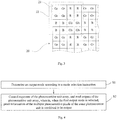
- FIG. 4 is a flow chart of a pixel information output method of an image sensor, in accordance with one embodiment of the present disclosure. As shown in FIG. 4 , the mehtod includes the following steps to:
- the output module includes a first output mode and a second output mode.
- the first mode can be understood as an output mode for improving the imaging sensitivity and the SNR.
- the second mode can be understood as an output mode for the phase foucing and the depth information test.
- the combined output signal of the plurality of photosensitive pixels is improved by N times. Since the noise is proportional to the square root of the signal, that is, noise ⁇ (Signal) 1/2 , the signal becomes N times than ever, the noise is N 1/2 times than ever, and both the imaging sensitivity and the SNR of the image have a corresponding improvement.
- FIG. 5 is a shcematic diagram of imaging light in accrodance with one embodiment of the present disclosure. Wherein, one micro-lens corresponds to one filter cell and four photosensitive pixels.
- FIG. 6 is a shcematic diagram of imaging light of the related art. Wherein, one micro-lens corresponds to one filter cell and one photosensitive pixel. As shown in FIG. 1 and FIG. 5 , if the pixel information of the four photosensitive pixels is combined to be output, the signal will becomes 4 times than that of the pixel struture shown in FIG. 6 , and noise will be only 2 times than that of the pixel struture shown in FIG. 6 , thus both the sensitivity and the SNR of the image have a corresponding improvement.
- the pixel information output method of the image sensor of the embodiment of the present disclosure based on the structure in which one micro-lens corresponds to one filter cell and a plurality of photosensitive pixels, makes the pixel information of the plurality of photosensitive pixels of the same photosensitive unit be combined to be output, when the first output mode is selected. Compared with the output of a single photosensitive pixel of the related art, this can improve the imaging sensitivity and the SNR to improve the image quality.
- the pixel information of the plurality of photosensitive pixels of the same photosensitive unit is controlled to be individually output. And then, the imaging light can be distinguished to obtain the phase difference information of imaging according to the pixel information of the plurality of photosensitive pixels of the photosensitive unit, and the phase focusing can be adjusted according to the phase difference information.
- the imaging light passes through the micro-lens and is then converged on the photosensitive pixel to be imaged, in the case of focus as shown in FIG. 7(1) .
- the imaging light diverges, and each micro-lens receives the divergence light from serveal directions to be imaged by the corresponding photosensitive pixels below. Because the same photosensitive pixel cannot distinguish direction of the received light, the condition of the relative detection can not be met.
- the masked pixel in order to achieve the PDAF (Phase Detection Auto Focus), physical design of pairs of adjacent photosensitive pixels (a.k.a. masked pixels, the masked pixel has a more complicated structure than an ordinary photosensitive pixel.
- the masked pixels are usually arranged in pairs, proximity, and symmetry.
- the pairs of masked pixels are used to split the light from several directions) in the image sensor is used to split the imaging light, toward the pairs of masked pixels and from several directions, into left and right two parts.
- the distance, which the camera lens needs to be moved, can be calculated by means of comparing the phase differences (that is, by collecting outputs of the pairs of the masked pixels) after imaging using the light of the left and right parts.
- each micro-lens corresponds to a filter cell and a photosensitive unit
- each photosensitive unit includes a plurality of photosensitive pixels, that is, each micro-lens corresponds to a plurality of photosensitive pixels. Therefore, the light received by each micro-lens is used to be imaged by the plurality of photosensitive pixels.
- the pixel information of the plurality of photosensitive pixels of the same photosensitive unit is controlled to be individually output, so that light signals from several directions can be captured. It can be seen that the above structure plays a role in splitting the imaging light. And then, the imaging light can be identified according to the pixel information output of the plurality of photosensitive pixels of each photosensitive unit.
- the phase difference information of the image can be obtained by comparing the light signals from different directions. Futhermore, the distance of a shooting object is captured according to the phase difference information, and a data basis is provided for the phase focusing and the depth information test.
- the relative focusing detection can be achieved only by cooperative design among the micro-lens unit, the filter cell, and the photosensitive unit. Thus, there is no need to change the structure of the ordinary photosensitive pixel or increase a light mask on the structure of the ordinary photosensitive pixel alone, and the approach to realize the relative focusing detection is easier.
- the light signals from different diections i.e. up, down, left, right light signals
- the phase difference information of the whole image can be obtained by comparing the light signals from different directions.
- the phase difference information can be converted into the focusing distance information, and the phase focusing can be achieved by means of adjusting the position of the camera lens in accordance with the focusing distance information.
- the pixel information output method of the image sensor of the embodiment of the present disclosure based on an arrangement that each micro-lens corresponds to the plurality of photosensitive pixels, two work states can be achieved.
- the first work state is that the pixel information of the plurality of photosensitive pixels of each photosensitive unit is combined to be output to improve the image quality.
- Another work state is that the pixel information of the plurality of photosensitive pixels of each photosensitive unit is individually output, and the phase difference information can be obtained by comparing the information among the photosensitive pixels, thereby providing a data basis for the phase focusing and the depth information test.
- phase focusing method of an embodiment of the present disclosure is explaned below.
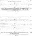
- FIG. 8 is a flow chart of a phase focusing method, according to an embodiment of the present disclosure. As shown in FIG. 8 , the phase focusing method includes the following steps to:
- the image sensor includes a photosensitive unit array, a filter array, and a micro-lens array.
- the filter array is arranged on the photosensitive unit array.
- the micro-lens array is arranged above the filter array.
- Each micro-lens covers a filter cell and a photosensitive unit.
- Each photosensitive unit includes a plurality of photosensitive pixels, which means each micro-lens corresponds to a plurality of photosensitive pixels.
- the phase focusing method of the present disclosure based on the structure of the image sensor in which each micro-lens corresponds to one filter cell and a plurality of photosensitive pixels, makes the pixel information of the plurality of photosensitive pixels of the same photosensitive unit individually output.
- each photosensitive unit can obtain light signals from different directions to provide a condition for the phase focusing, and then the phase difference information can be obtained to realize the phase focusing.
- An imaging device of an embodiment of the present disclosure, of another aspect, is explaned below.
- FIG. 9 is a block diagram of an imaging device, according to an embodiment of the present disclosure. As shown in FIG. 9 , the imaging device 1000 includes the above-mentioned image sensor 100 and a control module 200.
- the control module 200 determines an output mode according to a mode selection instruction, controls the exposure of the photosensitive unit array, and outputs of the photosensitive unit array are read. Wherein, when the first output mode is selected, the control module 200 controls the pixel information of the plurality of photosensitive pixels of a same photosensitive unit to be combined to be output.
- the imaging device of the present disclosure based on the structure of the image sensor in which each micro-lens corresponds to one filter cell and a plurality of photosensitive pixels, the control module makes the pixel information of the photosensitive pixels of the same photosensitive unit be combined to be output, when the first output mode is selected. Compared with the output of the single photosensitive unit of the related art, this can improve the imaging sensitivity and the SNR to improve the image quality.
- the control module 200 controls the pixel information of the photosensitive pixels of the same photosensitive unit to be individually output.
- the control module 200 distinguishes the imaging light to obtain phase difference information of imaging according to the pixel information of the photosensitive pixels of the photosensitive unit, and adjusts the phase focusing according to the phase difference information.
- the terminal 2000 includes the imaging device 1000 of the above-mentioned embodiment.
- the terminal 2000 can take a picture, and have an improving image quality and a phase detection funciton.
- the imaging device 100 includes an image sensor 100 and a control moudle 200.
- the control module 200 controls the exposure of the photosensitive unit array of the image sensor 100, and the outputs of the photosensitive unit array are read. Wherein, the control module 200 controls the pixel information of the photosensitive pixels of the same photosensitive unit to be individually output, distinguishes the imaging light to obtain phase difference information of imaging according to the pixel information of the plurality of photosensitive pixels of the photosensitive unit, and adjusts the phase focusing according to the phase difference information.
- the control module 200 makes the pixel information of the photosensitive pixels of the same photosensitive unit be individually output.
- each photosensitive unit can obtain light signals from different directions to provide a condition for the phase focusing, and then the phase difference information can be obtained to provide a basis for realizing the phase focusing.
- a terminal 2000 of an embodiment of the present disclosure, of another aspect, is described below referring to the figures.
- the terminal 2000 includes the imaging device 1000 of the above-mentioned embodiment.
- the terminal 2000 has a phase focusing funciton.
- the terminal 2000 can include, but is not limted to, cell phones.
- the imaging device 1000 can include a front-facing camera(s), obtain focusing distance information according to the phase difference information, and then adjust the distance of the front-facing camera according to the focusing distance information to realize the phase focusing.
- the image sensor includes a photosensitive unit array, a filter cell array, and a micro-lens array.
- the filter cell array is arranged on the photosensitive unit array.
- the micro-lens array is arranged above the filter cell array.
- Each micro-lens covers a filter cell and a photosensitive unit.
- Each photosensitive unit includes a plurality of photosensitive pixels.
- FIG. 11 is a flow chart of an imaging method, according to an embodiment of the present disclosure. As shown in FIG. 9 , the imaging method includes the following steps to:
- the imaging method of the embodiment of the present disclosure assuming the output of each oringal photosensitive unit is represented as S, the noise is represented as N, the photosensitive unit includes M photosensitive units, the pixel value of the photosensitive unit can be represented as n*m*S, and the noise of the photosensitive unit is represented as n * m * N 2 n * m .
- the noise of the photosensitive unit is about n*m*N/2. Therefore, the brightness of the photosensitive unit in a low-luminance environment is improved, and the SNR is improved.
- each photosensitive unit includes 2*2 photosensitive pixels.
- the image sensor 100 includes a register, the step of S2 further includes:
- the step of S2 further includes:
- an image processing module as a digital signal processing chip can directly process outputs of the image sensor, and compared with some solutions of directly processing the outputs of the image sensor with an analog signal format through a circuit, the image information is better reserved.
- the imaging method of the present disclosure can both produce a megered image with 4M pixles (which combines the 2*2 pixels), and produce an orginal image with 16M pixels (which is not combined).
- a mobile terminal of an embodiment of the present disclosure in another aspect, is provided.
- the terminal includes a housing, a proceesor, a storage, a circuit board, and a power circuit.
- the circuit board is positioned inside a space surrouded by the housing.
- the processor and the stroage are disposed on the circuit board.
- the power circuit is configured to supply power for each electric circuit or component of the mobile terminal.
- the storage is configured to store executable program codes.
- the processor executes a program corresponding to the executable program codes, by means of reading the executable program codes stored in the storage, for executing the above-mentioned imaging method.
- a computer-readable storage medium of an embodiment of the present disclosure is also provided.
- the computer-readable storage medium includes instructions stored therein.
- the mobile terminal executes the imaging method of the embodiments of the present disclosure, as shown in FIG. 11 .
- the logic and/or steps described in other manners herein or shown in the flow chart, for example, a particular sequence table of executable instructions for realizing the logical function may be specifically achieved in any computer-readable medium to be used by the instruction execution system, device or equipment (such as the system based on computers, the system comprising processors or other systems capable of obtaining the instruction from the instruction execution system, device and equipment and executing the instruction), or to be used in combination with the instruction execution system, device and equipment.
- the computer-readable medium may be any device adaptive for including, storing, communicating, propagating or transferring programs to be used by or in combination with the instruction execution system, device or equipment.
- the computer-readable medium comprise but are not limited to: an electronic connection (an electronic device) with one or more wires, a portable computer enclosure (a magnetic device), a random access memory (RAM), a read only memory (ROM), an erasable programmable read-only memory (EPROM or a flash memory), an optical fiber device, and a portable compact disk read-only memory (CDROM).
- the computer readable medium may even be a paper or other appropriate medium capable of printing programs thereon, this is because, for example, the paper or other appropriate medium may be optically scanned and then edited, decrypted or processed with other appropriate methods when necessary to obtain the programs in an electric manner, and then the programs may be stored in the computer memories.
- each part of the present disclosure may be realized by the hardware, software, firmware or their combination.
- a plurality of steps or methods may be realized by the software or firmware stored in the memory and executed by the appropriate instruction execution system.
- the steps or methods may be realized by one or a combination of the following techniques known in the art: a discrete logic circuit having a logic gate circuit for realizing a logic function of a data signal, an application-specific integrated circuit having an appropriate combination logic gate circuit, a programmable gate array (PGA), a field programmable gate array (FPGA), etc.
Landscapes
- Engineering & Computer Science (AREA)
- Multimedia (AREA)
- Signal Processing (AREA)
- Studio Devices (AREA)
- Automatic Focus Adjustment (AREA)
- Transforming Light Signals Into Electric Signals (AREA)
- Solid State Image Pick-Up Elements (AREA)
- Focusing (AREA)
- Color Television Image Signal Generators (AREA)
Applications Claiming Priority (2)
| Application Number | Priority Date | Filing Date | Title |
|---|---|---|---|
| CN201510963242.5A CN105611122B (zh) | 2015-12-18 | 2015-12-18 | 图像传感器及输出方法、相位对焦方法、成像装置和终端 |
| PCT/CN2016/101704 WO2017101572A1 (fr) | 2015-12-18 | 2016-10-10 | Capteur d'image, et procédé de sortie, procédé de focalisation de phase, appareil d'imagerie, et terminal |
Publications (2)
| Publication Number | Publication Date |
|---|---|
| EP3236647A1 true EP3236647A1 (fr) | 2017-10-25 |
| EP3236647A4 EP3236647A4 (fr) | 2018-01-10 |
Family
ID=55990638
Family Applications (1)
| Application Number | Title | Priority Date | Filing Date |
|---|---|---|---|
| EP16874631.1A Ceased EP3236647A4 (fr) | 2015-12-18 | 2016-10-10 | Capteur d'image, et procédé de sortie, procédé de focalisation de phase, appareil d'imagerie, et terminal |
Country Status (11)
| Country | Link |
|---|---|
| US (2) | US10880501B2 (fr) |
| EP (1) | EP3236647A4 (fr) |
| JP (1) | JP2018509061A (fr) |
| KR (1) | KR102038680B1 (fr) |
| CN (1) | CN105611122B (fr) |
| AU (1) | AU2016370348B2 (fr) |
| MY (1) | MY184812A (fr) |
| SG (1) | SG11201706245YA (fr) |
| TW (2) | TWI612811B (fr) |
| WO (1) | WO2017101572A1 (fr) |
| ZA (1) | ZA201706228B (fr) |
Families Citing this family (26)
| Publication number | Priority date | Publication date | Assignee | Title |
|---|---|---|---|---|
| CN105611122B (zh) | 2015-12-18 | 2019-03-01 | Oppo广东移动通信有限公司 | 图像传感器及输出方法、相位对焦方法、成像装置和终端 |
| CN106454288B (zh) * | 2016-11-29 | 2018-01-19 | 广东欧珀移动通信有限公司 | 控制方法、控制装置、成像装置及电子装置 |
| CN106504218B (zh) | 2016-11-29 | 2019-03-12 | Oppo广东移动通信有限公司 | 控制方法、控制装置及电子装置 |
| CN106341670B (zh) | 2016-11-29 | 2017-09-22 | 广东欧珀移动通信有限公司 | 控制方法、控制装置及电子装置 |
| CN106454054B (zh) * | 2016-11-29 | 2019-03-19 | Oppo广东移动通信有限公司 | 控制方法、控制装置及电子装置 |
| CN107040702B (zh) * | 2017-04-28 | 2020-06-05 | Oppo广东移动通信有限公司 | 图像传感器、对焦控制方法、成像装置和移动终端 |
| CN106982329B (zh) * | 2017-04-28 | 2020-08-07 | Oppo广东移动通信有限公司 | 图像传感器、对焦控制方法、成像装置和移动终端 |
| CN107155072A (zh) * | 2017-04-28 | 2017-09-12 | 广东欧珀移动通信有限公司 | 全景拍摄方法、装置和终端设备 |
| CN107040730B (zh) * | 2017-04-28 | 2020-05-08 | Oppo广东移动通信有限公司 | 图像传感器的成像控制方法、图像传感器,以及成像装置 |
| CN107147845B (zh) * | 2017-04-28 | 2020-11-06 | Oppo广东移动通信有限公司 | 对焦方法、装置和终端设备 |
| CN107105141B (zh) * | 2017-04-28 | 2019-06-28 | Oppo广东移动通信有限公司 | 图像传感器、图像处理方法、成像装置和移动终端 |
| CN107135340A (zh) * | 2017-04-28 | 2017-09-05 | 广东欧珀移动通信有限公司 | 图像传感器、对焦控制方法、成像装置和移动终端 |
| US10714520B1 (en) * | 2017-08-04 | 2020-07-14 | Facebook Technologies, Llc | Manufacturing an on-chip microlens array |
| US10777609B1 (en) * | 2019-04-01 | 2020-09-15 | Visera Technologies Company Limited | Optical devices with light collection elements formed in pixels |
| CN110381181A (zh) * | 2019-06-28 | 2019-10-25 | 信利光电股份有限公司 | 前置距离感应方法、电子装置、存储介质和移动终端 |
| CN111131714A (zh) * | 2019-12-31 | 2020-05-08 | 联想(北京)有限公司 | 图像采集控制方法、装置及电子设备 |
| US11663728B2 (en) | 2020-01-16 | 2023-05-30 | Samsung Electronics Co., Ltd. | Depth estimation method and apparatus |
| CN111464733B (zh) * | 2020-05-22 | 2021-10-01 | Oppo广东移动通信有限公司 | 控制方法、摄像头组件和移动终端 |
| CN112243096B (zh) * | 2020-09-30 | 2024-01-02 | 格科微电子(上海)有限公司 | 像素合成模式下的像素读取方法及装置、存储介质、图像采集设备 |
| CN112616009B (zh) * | 2020-12-31 | 2022-08-02 | 维沃移动通信有限公司 | 电子设备及其摄像模组 |
| US12556785B2 (en) * | 2021-02-20 | 2026-02-17 | Boe Technology Group Co., Ltd. | Image acquisition device, image acquisition apparatus, image acquisition method and manufacturing method |
| CN113654459B (zh) * | 2021-07-22 | 2024-05-24 | 北京小米移动软件有限公司 | 一种屏下感光传感器位置确定方法、装置及存储介质 |
| KR102928805B1 (ko) | 2021-08-31 | 2026-02-23 | 삼성전자주식회사 | 영상 처리 방법 및 장치 |
| CN114650369B (zh) * | 2022-03-01 | 2025-01-07 | 维沃移动通信有限公司 | 成像方法和装置 |
| CN114827488B (zh) * | 2022-04-26 | 2023-02-17 | 北京大学 | 像素结构单元、像素结构阵列及其操作方法、图像传感器 |
| KR20240045876A (ko) | 2022-09-30 | 2024-04-08 | 삼성전자주식회사 | 오토 포커싱을 위한 이미징 장치 및 방법 |
Family Cites Families (26)
| Publication number | Priority date | Publication date | Assignee | Title |
|---|---|---|---|---|
| US6999119B1 (en) * | 1998-04-10 | 2006-02-14 | Nikon Corporation | Image-capturing element, image-capturing circuit for processing signal from image-capturing element, image-capturing device, driving method of image-capturing element |
| JP2004191630A (ja) * | 2002-12-11 | 2004-07-08 | Canon Inc | 撮像装置 |
| US7568628B2 (en) | 2005-03-11 | 2009-08-04 | Hand Held Products, Inc. | Bar code reading device with global electronic shutter control |
| KR100976284B1 (ko) * | 2007-06-07 | 2010-08-16 | 가부시끼가이샤 도시바 | 촬상 장치 |
| US7745779B2 (en) * | 2008-02-08 | 2010-06-29 | Aptina Imaging Corporation | Color pixel arrays having common color filters for multiple adjacent pixels for use in CMOS imagers |
| US8134115B2 (en) * | 2009-06-23 | 2012-03-13 | Nokia Corporation | Color filters for sub-diffraction limit-sized light sensors |
| DE102009049387B4 (de) * | 2009-10-14 | 2016-05-25 | Fraunhofer-Gesellschaft zur Förderung der angewandten Forschung e.V. | Vorrichtung, Bildverarbeitungsvorrichtung und Verfahren zur optischen Abbildung |
| CN102870028B (zh) * | 2010-04-28 | 2015-11-25 | 富士胶片株式会社 | 成像装置 |
| KR101777351B1 (ko) * | 2011-05-16 | 2017-09-11 | 삼성전자주식회사 | 촬상 소자, 이를 이용한 디지털 촬영 장치, 오토 포커싱 방법, 및 상기 방법을 수행하기 위한 컴퓨터 판독가능 저장매체 |
| JP2013066140A (ja) * | 2011-08-31 | 2013-04-11 | Sony Corp | 撮像装置、および信号処理方法、並びにプログラム |
| CN102510450A (zh) * | 2011-10-17 | 2012-06-20 | 北京瑞澜联合通信技术有限公司 | 图像传感器、摄像装置及图像数据生成方法 |
| TWI504251B (zh) * | 2012-07-04 | 2015-10-11 | Vivotek Inc | 攝像裝置在對焦時的提示聲音之處理方法 |
| JP6010465B2 (ja) * | 2013-01-11 | 2016-10-19 | 富士フイルム株式会社 | 固体撮像装置 |
| JP6271842B2 (ja) * | 2013-02-18 | 2018-01-31 | キヤノン株式会社 | 測距装置、測距方法、および撮像装置 |
| US10136090B2 (en) * | 2013-03-15 | 2018-11-20 | Rambus Inc. | Threshold-monitoring, conditional-reset image sensor |
| JP6220148B2 (ja) | 2013-04-26 | 2017-10-25 | キヤノン株式会社 | 撮像装置およびその制御方法 |
| JP6639385B2 (ja) | 2013-06-11 | 2020-02-05 | ラムバス・インコーポレーテッド | スプリットゲート条件付きリセットイメージセンサ |
| CN103531603B (zh) * | 2013-10-30 | 2018-10-16 | 上海集成电路研发中心有限公司 | 一种cmos图像传感器 |
| WO2015083683A1 (fr) * | 2013-12-05 | 2015-06-11 | オリンパス株式会社 | Dispositif d'imagerie et procédé de commande du dispositif d'imagerie |
| CN103686103B (zh) * | 2013-12-31 | 2018-01-26 | 上海集成电路研发中心有限公司 | 具有合并和分裂模式的图像传感器、像素单元 |
| JP6338436B2 (ja) * | 2014-04-25 | 2018-06-06 | キヤノン株式会社 | 撮像装置及びその制御方法 |
| CN104064577A (zh) * | 2014-07-16 | 2014-09-24 | 上海集成电路研发中心有限公司 | 自动对焦的图像传感器 |
| JP6369233B2 (ja) * | 2014-09-01 | 2018-08-08 | ソニー株式会社 | 固体撮像素子及びその信号処理方法、並びに電子機器 |
| CN104241310B (zh) * | 2014-09-23 | 2017-11-07 | 上海集成电路研发中心有限公司 | 一种具有双微透镜层的cmos图像像素阵列 |
| KR102390836B1 (ko) * | 2015-10-05 | 2022-04-26 | 삼성전자주식회사 | 이미지 데이터를 생성하는 전자 장치 및 방법 |
| CN105611122B (zh) * | 2015-12-18 | 2019-03-01 | Oppo广东移动通信有限公司 | 图像传感器及输出方法、相位对焦方法、成像装置和终端 |
-
2015
- 2015-12-18 CN CN201510963242.5A patent/CN105611122B/zh active Active
-
2016
- 2016-10-10 WO PCT/CN2016/101704 patent/WO2017101572A1/fr not_active Ceased
- 2016-10-10 JP JP2017541007A patent/JP2018509061A/ja active Pending
- 2016-10-10 KR KR1020177026269A patent/KR102038680B1/ko not_active Expired - Fee Related
- 2016-10-10 EP EP16874631.1A patent/EP3236647A4/fr not_active Ceased
- 2016-10-10 AU AU2016370348A patent/AU2016370348B2/en active Active
- 2016-10-10 MY MYPI2017702798A patent/MY184812A/en unknown
- 2016-10-10 SG SG11201706245YA patent/SG11201706245YA/en unknown
- 2016-12-15 TW TW105141603A patent/TWI612811B/zh active
- 2016-12-15 TW TW106142226A patent/TWI662842B/zh active
-
2017
- 2017-06-26 US US15/632,697 patent/US10880501B2/en active Active
- 2017-09-13 ZA ZA2017/06228A patent/ZA201706228B/en unknown
-
2019
- 2019-06-09 US US16/435,555 patent/US10764522B2/en active Active
Also Published As
| Publication number | Publication date |
|---|---|
| TWI612811B (zh) | 2018-01-21 |
| US20170295332A1 (en) | 2017-10-12 |
| WO2017101572A1 (fr) | 2017-06-22 |
| TW201818716A (zh) | 2018-05-16 |
| TW201724842A (zh) | 2017-07-01 |
| CN105611122A (zh) | 2016-05-25 |
| CN105611122B (zh) | 2019-03-01 |
| EP3236647A4 (fr) | 2018-01-10 |
| ZA201706228B (en) | 2019-01-30 |
| JP2018509061A (ja) | 2018-03-29 |
| US10880501B2 (en) | 2020-12-29 |
| AU2016370348A1 (en) | 2017-08-10 |
| KR102038680B1 (ko) | 2019-10-30 |
| SG11201706245YA (en) | 2017-08-30 |
| AU2016370348B2 (en) | 2018-06-28 |
| MY184812A (en) | 2021-04-23 |
| TWI662842B (zh) | 2019-06-11 |
| KR20170120134A (ko) | 2017-10-30 |
| US20190297288A1 (en) | 2019-09-26 |
| US10764522B2 (en) | 2020-09-01 |
Similar Documents
| Publication | Publication Date | Title |
|---|---|---|
| US10764522B2 (en) | Image sensor, output method, phase focusing method, imaging device, and terminal | |
| EP3396942B1 (fr) | Détecteur d'images, procédé d'imagerie et dispositif électronique | |
| US11108943B2 (en) | Image sensor, focusing control method, and electronic device | |
| US10257447B2 (en) | Imaging method, imaging device, and electronic device | |
| EP3693768B1 (fr) | Capteur d'image de focalisation à double noyau, son procédé de commande de focalisation et dispositif électronique | |
| US10594962B2 (en) | Image sensor, imaging device, mobile terminal and imaging method for producing high resolution image | |
| US9979883B2 (en) | Imaging method for image sensor, imaging apparatus, and electronic device | |
| US10270988B2 (en) | Method for generating high-dynamic range image, camera device, terminal and imaging method | |
| US10893187B2 (en) | Dual-core focusing image sensor, control-focusing method therefor, and mobile terminal | |
| KR20240120602A (ko) | 이미지 센서를 통해서 이미지를 획득하는 전자 장치 및 그 동작 방법 | |
| US20240259680A1 (en) | Electronic device acquiring image through image sensor, and operating method thereof | |
| US20250111481A1 (en) | Training data, trained model, imaging apparatus, learning device, method of creating training data, and method of generating trained model |
Legal Events
| Date | Code | Title | Description |
|---|---|---|---|
| STAA | Information on the status of an ep patent application or granted ep patent |
Free format text: STATUS: THE INTERNATIONAL PUBLICATION HAS BEEN MADE |
|
| PUAI | Public reference made under article 153(3) epc to a published international application that has entered the european phase |
Free format text: ORIGINAL CODE: 0009012 |
|
| STAA | Information on the status of an ep patent application or granted ep patent |
Free format text: STATUS: REQUEST FOR EXAMINATION WAS MADE |
|
| 17P | Request for examination filed |
Effective date: 20170719 |
|
| AK | Designated contracting states |
Kind code of ref document: A1 Designated state(s): AL AT BE BG CH CY CZ DE DK EE ES FI FR GB GR HR HU IE IS IT LI LT LU LV MC MK MT NL NO PL PT RO RS SE SI SK SM TR |
|
| AX | Request for extension of the european patent |
Extension state: BA ME |
|
| A4 | Supplementary search report drawn up and despatched |
Effective date: 20171208 |
|
| RIC1 | Information provided on ipc code assigned before grant |
Ipc: H04N 5/225 20060101AFI20171204BHEP Ipc: H04N 5/347 20110101ALI20171204BHEP Ipc: H04N 5/369 20110101ALI20171204BHEP Ipc: H01L 27/146 20060101ALI20171204BHEP |
|
| STAA | Information on the status of an ep patent application or granted ep patent |
Free format text: STATUS: EXAMINATION IS IN PROGRESS |
|
| 17Q | First examination report despatched |
Effective date: 20181010 |
|
| DAV | Request for validation of the european patent (deleted) | ||
| DAX | Request for extension of the european patent (deleted) | ||
| RAP1 | Party data changed (applicant data changed or rights of an application transferred) |
Owner name: GUANGDONG OPPO MOBILE TELECOMMUNICATIONS CORP., LT |
|
| REG | Reference to a national code |
Ref country code: DE Ref legal event code: R003 |
|
| STAA | Information on the status of an ep patent application or granted ep patent |
Free format text: STATUS: THE APPLICATION HAS BEEN REFUSED |
|
| 18R | Application refused |
Effective date: 20210113 |