EP3237898B1 - Procédé pour la fabrication d'un dispositif detecteur de gaz pour détecter au moins un analyte gazeux dans un fluide de mesure, ainsi procédé et dispositif detecteur de gaz pour détecter au moins un analyte gazeux dans un fluide de mesure - Google Patents
Procédé pour la fabrication d'un dispositif detecteur de gaz pour détecter au moins un analyte gazeux dans un fluide de mesure, ainsi procédé et dispositif detecteur de gaz pour détecter au moins un analyte gazeux dans un fluide de mesure Download PDFInfo
- Publication number
- EP3237898B1 EP3237898B1 EP15807655.4A EP15807655A EP3237898B1 EP 3237898 B1 EP3237898 B1 EP 3237898B1 EP 15807655 A EP15807655 A EP 15807655A EP 3237898 B1 EP3237898 B1 EP 3237898B1
- Authority
- EP
- European Patent Office
- Prior art keywords
- semiconductor substrate
- chamber
- setting
- measurement medium
- detection
- Prior art date
- Legal status (The legal status is an assumption and is not a legal conclusion. Google has not performed a legal analysis and makes no representation as to the accuracy of the status listed.)
- Not-in-force
Links
Images






Classifications
-
- G—PHYSICS
- G01—MEASURING; TESTING
- G01N—INVESTIGATING OR ANALYSING MATERIALS BY DETERMINING THEIR CHEMICAL OR PHYSICAL PROPERTIES
- G01N27/00—Investigating or analysing materials by the use of electric, electrochemical, or magnetic means
- G01N27/26—Investigating or analysing materials by the use of electric, electrochemical, or magnetic means by investigating electrochemical variables; by using electrolysis or electrophoresis
- G01N27/403—Cells and electrode assemblies
- G01N27/406—Cells and probes with solid electrolytes
- G01N27/407—Cells and probes with solid electrolytes for investigating or analysing gases
- G01N27/4071—Cells and probes with solid electrolytes for investigating or analysing gases using sensor elements of laminated structure
Definitions
- the present invention relates to a method for producing a gas sensor device for detecting at least one gaseous analyte in a measuring medium, to a gas sensor device for detecting at least one gaseous analyte in a measuring medium, to a method for detecting at least one gaseous analyte in a measuring medium, on a corresponding device and to a corresponding computer program.
- Ceramic nitrogen oxide sensors for example zirconia-based sensors, in particular in motor vehicles, can be used to monitor or regulate exhaust aftertreatment systems.
- sensor elements can be manufactured by means of thick-film technology, wherein dimensions can be for example only about 4 millimeters by 50 millimeters by 3 millimeters. Due to such dimensions, ie due to the thermal mass, to achieve a necessary operating temperature, for example about 700 degrees Celsius, heating powers in the single-digit to double-digit watt range may be typical.
- the DE 10 2012 201304 A1 discloses a micromechanical solid electrolyte sensor device and a corresponding manufacturing method.
- the US 4,668,374 discloses a gas sensor and a method of manufacturing the same, wherein the gas sensor is manufactured by a microelectronics fabrication technique and comprises a plurality of thin film solid electrolyte cells for pumping and sensing in a hermetically sealed sensor chamber.
- a microelectrochemical gas sensor in particular a microelectrochemical nitrogen oxide sensor or a semiconductor-based thin-film gas sensor or nitrogen oxide sensor or dual-chamber nitrogen oxide sensor produced by means of microsystem technology
- semiconductor substrates can be processed microsystemically in order to manufacture such a sensor, or such a sensor can be manufactured from microsystem-technically processed semiconductor substrates.
- a functional principle can be realized with oxygen-ion-conducting functional ceramics as well as with a plurality of chambers.
- the invention relates to a method for producing a gas sensor device for detecting at least one gaseous analyte in a measuring medium, the method having the steps of independent claim 1.
- the gas sensor device may be configured to qualitatively and additionally or alternatively quantitatively detect at least one gaseous analyte.
- the at least one gaseous analyte may comprise, for example, oxygen and additionally or alternatively nitrogen oxides.
- the gas sensor device may be designed as a nitrogen oxide sensor.
- the gas sensor device can be used, for example, for exhaust gas sensors in motor vehicles, for exhaust gas sensors in, for example, stationary heating systems, for fire alarm systems, for gas sensors in mobile electronic devices, such as mobile telephones, for a respiratory gas analysis, for industrial process monitoring, etc.
- the gas sensor device can be used for example in motor vehicles and be configured to monitor exhaust gas aftertreatment systems.
- the measuring medium may be an exhaust gas or exhaust gas mixture of a motor vehicle, ambient air or the like.
- the semiconductor substrates may be formed of materials that can be processed by semiconductor processing processes.
- the solid electrolyte layers may comprise an ion-conducting, for example ceramic material, in particular an oxygen ion-conducting ceramic material.
- the at least one separation process may include trenching, etching, etc.
- the at least one coating process may include pulsed laser deposition (PLD), sputtering, atomic layer deposition (ALD), wet chemical deposition techniques, etc.
- PLD pulsed laser deposition
- ALD atomic layer deposition
- wet chemical deposition techniques etc.
- the semiconductor substrates may be joined so as to form, from at least a subset of the recessed portions, the adjustment chamber, the detection chamber, and the diffusion portion.
- a cohesive connection between the semiconductor substrates can be produced.
- high-temperature stable, hermetically sealing glasses can be used for connecting and sealing the semiconductor substrates.
- an adjustment device having a first solid electrolyte layer between a first pair of electrodes for adjusting a gas composition of the measurement medium with respect to a companion gas, a determination device having a second solid electrolyte layer between a second pair of electrodes for determining a content of the accompanying gas in the measuring medium and a detection device with a third solid electrolyte layer between a third electrode pair for detecting the gaseous analyte produced.
- the determining means, the adjusting means and the detecting means are galvanically separated from each other, so that in a joined state of the first semiconductor substrate and the second semiconductor substrate, the determining means and adjusting means are formed as wall portions of the adjusting chamber, and the Detection device is formed as a wall portion of the detection chamber.
- the at least one gaseous analyte may comprise, for example, nitrogen oxides and the associated gas may be oxygen.
- the determination device, the setting device and the detection device can also represent Nernst cells or pump cells.
- Such an embodiment offers the advantage that, on the one hand, the analyte can also be detected indirectly via the associated gas and, on the other hand, a particularly accurate and inexpensive detection of the at least one gaseous analyte is made possible.
- the determination device, the setting device and the detection device can be driven decoupled from each other due to their galvanically separated arrangement, resulting in an increased signal quality of a sensor signal Gas sensor device can lead.
- a common electric signal line may be connected to the adjustment chamber and electrodes arranged facing the detection chamber. Furthermore, in this case own electrical signal lines can be connected to remote from the adjustment chamber and the detection chamber arranged electrodes. Such an embodiment has the advantage that a cabling complexity of the gas sensor device can be reduced by the common signal line.
- At least one tempering device for tempering the solid electrolyte layers and additionally or alternatively the electrodes in a region of the first semiconductor substrate and additionally or alternatively in a region of the second semiconductor substrate can be arranged.
- the at least one tempering device can be designed as a microsystem membrane heater.
- an evaluation device can be integrated in a region of the first semiconductor substrate and additionally or alternatively in a region of the second semiconductor substrate.
- a signal quality can be further improved by shortening lead lengths from the electrodes to the evaluation device.
- the evaluation device or evaluation electronics can either be integrated into the gas sensor device, in particular directly on a sensor chip thereof, or alternatively can be arranged adjacent to the gas sensor device.
- a gas sensor device for detecting at least one gaseous analyte in a measuring medium is also presented, wherein the gas sensor device has the features of independent claim 5.
- the gas sensor device may be manufactured by carrying out an embodiment of the above-mentioned method.
- the first semiconductor substrate may include a first recessed portion for the adjustment chamber, a second recessed portion for the detection chamber, a third recessed portion for the diffusion portion between the first recessed portion and the second recessed portion, a fourth recessed portion for an access opening to the adjustment chamber for the measurement medium
- An adjusting device having a first solid electrolyte layer between a first pair of electrodes for adjusting a gas composition of the measuring medium with respect to an accompanying gas, the adjusting device being formed as a wall portion of the adjusting chamber in the first recessed portion, and a fifth recessed portion for the adjuster.
- the second semiconductor substrate may include a sixth recess portion for the adjustment chamber, a seventh recess portion for the detection chamber, a second solid electrolyte layer determiner between a second electrode pair for determining a content of an accompanying gas in the measurement medium, the determination means serving as a wall portion of the adjustment chamber in the second embodiment sixth recessed portion, a detection means having a third solid electrolyte layer between a third electrode pair for detecting the gaseous analyte, the detection means being formed as a wall portion of the detection chamber in the seventh recessed portion, an eighth recessed portion for the determiner and a ninth recessed portion for the detector ,
- Such an embodiment has the advantage that a particularly space-saving or miniaturized gas sensor device which can be produced cost-effectively and in large quantities can be provided with high detection accuracy.
- the method can thus be advantageously carried out in conjunction with an embodiment of the aforementioned gas sensor device in order to detect at least one gaseous analyte in a measuring medium.
- the approach presented here also creates a device that is designed to perform the steps of a variant of a method presented here in appropriate facilities to drive or implement. Also by this embodiment of the invention in the form of a device, the object underlying the invention can be solved quickly and efficiently.
- a device can be understood as meaning an electrical device which processes sensor signals and outputs control and / or data signals in dependence thereon.
- the device may have an interface, which may be formed in hardware and / or software.
- the interfaces can be part of a so-called system ASIC, for example, which contains a wide variety of functions of the device.
- the interfaces are separate, integrated circuits or at least partially made of discrete components consist.
- the interfaces may be software modules that are present, for example, on a microcontroller in addition to other software modules.
- a computer program product or computer program with program code which can be stored on a machine-readable carrier or storage medium such as a semiconductor memory, a hard disk memory or an optical memory and for carrying out, implementing and / or controlling the steps of the method according to one of the embodiments described above is used, especially when the program product or program is executed on a computer or a device.
- an embodiment of the aforementioned gas sensor device in microsystem technology can be used as a platform to integrate and evaluate combined sensor functions such as pressure detection, particle detection, lambda sensors, hydrocarbon detection, etc., on a single chip.
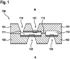
- Fig. 1 shows a schematic sectional view of a gas sensor device 100 according to an embodiment of the present invention.
- the gas sensor device 100 is designed to detect at least one gaseous analyte in a measurement medium M.
- the gas sensor device 100 is designed to detect, for example, nitrogen oxides in an exhaust gas of a motor vehicle.
- the at least one gaseous analyte comprises nitrogen oxides by way of example.
- the gas sensor device 100 is partially disposed in the measuring medium M and partially in a reference medium R and in reference air, for example, ambient air, arranged.
- the gas sensor device 100 can be arranged at a place of use such that a first side of the gas sensor device 100 faces the measuring medium M and a second side of the gas sensor device 100 faces the reference medium R.
- the reference medium can also be designed as a closed or partially closed reference space.
- the gas sensor device 100 has a first semiconductor substrate 101 and a second semiconductor substrate 102.
- the first semiconductor substrate 101 and the second semiconductor substrate 102 are formed of silicon, for example.
- the first semiconductor substrate 101 and the second semiconductor substrate 102 are joined together or materially connected to one another, for example by bonding, wafer bonding, gluing or the like.
- the first semiconductor substrate 101 faces or faces the measuring medium M
- the second semiconductor substrate 102 faces the reference medium R or is arranged such that it can be turned.
- an adjustment chamber 111 is formed.
- the adjustment chamber 111 is designed to set a gas composition of the measurement medium M or to allow adjustment of the gas composition of the measurement medium M.
- a detection chamber 112 is disposed or formed.
- the detection chamber 112 is configured to detect the gaseous analyte or to detect the gaseous analyte enable.
- a diffusion portion 113 and a diffusion barrier, respectively, are formed.
- the diffusion portion 113 is formed to control diffusion of the measurement medium M between the adjustment chamber 111 and the detection chamber 112.
- the adjustment chamber 111 and the detection chamber 112 are fluidly connected to each other by means of the diffusion section 113.
- the diffusion section 113 is a gap or the like in a wall between the adjustment chamber 111 and the detection chamber 112.
- an access opening 114 for accessing the measurement medium M or for gas entry into the adjustment chamber 111 is disposed formed.
- the adjustment chamber 111 is accessible via the inlet opening 114 for the measuring medium M.
- the access opening 114 can in this case be designed so that it also acts as a diffusion barrier.
- the adjustment chamber 111, the detection chamber 112 and the diffusion portion 113 are disposed between the assembled semiconductor substrates 101 and 102.
- the adjustment chamber 111, the detection chamber 112 and the diffusion section 113 are produced using at least one separation process, in particular a process from the field of semiconductor technology, micromachining, etc.
- the gas sensor device 100 comprises recessed sections, solid electrolyte layers and electrodes produced using at least one separation process and at least one coating process, which are described with reference to the gas sensor device 100 according to the method of FIG Fig. 1 illustrated embodiment of the present invention below with reference to the FIGS. 2A to 4G are described in more detail.
- an adjusting device 121 is arranged or generated.
- the adjusting device 121 is formed as a wall portion of the adjustment chamber 111.
- the adjusting device 121 has a first solid electrolyte layer and a first pair of electrodes. In this case, the first solid electrolyte layer is arranged between the first electrode pair.
- the adjusting device 121 is designed to be a gas composition of the Adjusting the measuring medium M in the adjustment chamber 111 with respect to an accompanying gas in the measuring medium M.
- a determination device 122 is arranged or generated.
- the determination device 122 is formed as a further wall section of the adjustment chamber 111.
- the determination device 122 has a second solid electrolyte layer and a second electrode pair. In this case, the second solid electrolyte layer is arranged between the second electrode pair.
- the determination device 122 is designed to determine a content of the accompanying gas in the measurement medium M in the adjustment chamber 111.
- a detection device 123 is arranged or generated on the second semiconductor substrate 102.
- the detection device 123 is formed as a wall portion of the detection chamber 112.
- the detection device 123 has a third solid electrolyte layer and a third electrode pair.
- the third solid electrolyte layer is arranged between the third electrode pair.
- the detection device 123 is designed to detect the gaseous analyte in the detection chamber 112.
- the gas sensor device 100 also includes the adjuster 121, the determiner 122, and the detector 123.
- the setting device 121, the determination device 120 and the detection device 123 are arranged galvanically separated from each other.
- the gas sensor device 100 may have at least one tempering device for tempering the solid electrolyte layers and additionally or alternatively the electrodes.
- a tempering device may be arranged in a region of the first semiconductor substrate 101 and additionally or alternatively in a region of the second semiconductor substrate 102.
- the gas sensor device 100 can also have an evaluation device for evaluating signals from the setting device 121, the determination device 122 and the detection device 123.
- Such an evaluation device may be in a region of the first semiconductor substrate 101 and additionally or Alternatively, be integrated or arranged in a region of the second semiconductor substrate 102.
- the gas sensor device 100 may include a common electrical signal line connectable to electrodes disposed on the adjustment chamber and the detection chamber, and a plurality of individual electrical signal leads connectable to electrodes remote from the adjustment chamber and the detection chamber.
- FIG. 2A shows a schematic sectional view of the first semiconductor substrate 101 of the gas sensor device Fig. 1 ,
- the first semiconductor substrate 101 is shown separately from the second semiconductor substrate of the gas sensor device.
- the first semiconductor substrate 101 is in FIG Fig. 2A shown in more detail. Illustrations regarding manufacturing steps of the first semiconductor substrate 101 are given with reference to FIGS. 3A to 3H shown and described in more detail.
- the setting device 121 displays the first solid electrolyte layer 221A and the first electrode pair with a first inner electrode 221B disposed on the first solid electrolyte layer 221A side of the adjustment chamber and a first outer electrode 221C disposed on the first solid electrolyte layer 221A side of the measurement medium.
- a first recessed portion 231 for the adjustment chamber From a side of the first semiconductor substrate 101 connectable to the second semiconductor substrate, in the first semiconductor substrate 101, a first recessed portion 231 for the adjustment chamber, a second recessed portion 232 for the detection chamber and between the first recessed portion 231 and the second recessed portion 232, a third recessed portion 233 for formed or generated the diffusion portion, for example by trenches and etching.
- a fourth recess section 234 for the access opening 114 to the adjustment chamber is provided in the first semiconductor substrate 101 and a fifth recess portion 235 for the adjuster 121 is formed, for example, by trenching and etching.
- the fourth recess section 234 and the fifth recess section 235 are arranged in the region of the first recess section 231 relative to a main extension plane of the first semiconductor substrate 101.
- the adjuster 121 is disposed in the first recessed portion 231 and the fifth recessed portion 235 as a wall portion of the adjusting chamber, for example, by depositing the first solid electrolyte layer 221A and the first inner electrode 221B from sides of the first recessed portion 231 and depositing the first outer electrode 221C Side of the fifth recess portion 235 from.
- a plurality of subsections of at least one etch stop layer 240 of the gas sensor device are shown in the region of the first semiconductor substrate 101.
- the etch stop layer 240 is arranged or applied to the first semiconductor substrate 101 on a side of the first semiconductor substrate 101 which can be turned on the measurement medium, outside a region of the recess sections 234 and 235. Further, the etch stop layer 240 is disposed on a side of the first semiconductor substrate 101 connectable to the second semiconductor substrate except for a portion of the first outside electrode 221C between the first solid electrolyte layer 221A and the first semiconductor substrate 101.
- FIG. 2B shows a schematic sectional view of the second semiconductor substrate 102 of the gas sensor device Fig. 1 ,
- the second semiconductor substrate 102 is shown separately from the first semiconductor substrate of the gas sensor device.
- the second semiconductor substrate 102 is in FIG Fig. 2B shown in more detail. Illustrations regarding manufacturing steps of the second semiconductor substrate 102 are described with reference to FIGS. 4A to 4G shown and described in more detail.
- the second solid electrolyte layer 222A and the second electrode pair are disposed with one side of the adjustment chamber at the second solid electrolyte layer 222A second inner electrode 222B and a second outer electrode 222C disposed on the side of the reference medium on the second solid electrolyte layer 222A.
- the detection means 123 displays the third solid electrolyte layer 223A and the third electrode pair with a third inner electrode 223B disposed on the third solid electrolyte layer 223A side of the detection chamber and a third outer electrode 223C disposed on the third solid electrolyte layer 223A side of the reference medium.
- a sixth recess portion 236 for the adjustment chamber and a seventh recess portion 237 for the detection chamber are formed in the second semiconductor substrate 102, for example, by trenching and etching.
- an eighth recessed portion 238 for the determiner 122 and a ninth recessed portion 239 for the detector 123 are formed in the second semiconductor substrate 102, for example, by trenching and etching.
- the eighth recess section 238 is arranged in the region of the sixth recess section 236 relative to a main extension plane of the second semiconductor substrate 102, wherein the ninth recess section 239 is arranged in the region of the seventh recess section 237 relative to a main extension plane of the second semiconductor substrate 102.
- the determining means 122 is disposed in the sixth recessed portion 236 and the eighth recessed portion 238 as a wall portion of the adjusting chamber, for example, by depositing the second solid electrolyte layer 222A and the second inner electrode 222B from the sixth recessed portion 236 side and depositing the second outer electrode 222C of FIG Sides of the eighth recess portion 238.
- the detector 123 is disposed in the seventh recess portion 237 and the ninth recess portion 239 as a wall portion of the detection chamber, for example, by depositing the third solid electrolyte layer 223A and the third inner electrode 223B from sides of the seventh recess portion 237 and depositing the third outer electrode 223C Pages of the ninth recess portion 239.
- a plurality of subsections of at least one etch stop layer 240 of the gas sensor device are shown in the region of the second semiconductor substrate 102.
- the etching stop layer 240 is disposed on a side of the second semiconductor substrate 102 which can be turned on the reference medium outside a region of the recess sections 238 and 239 on the second semiconductor substrate 102.
- the etching stopper layer 240 is provided on a side of the second semiconductor substrate 102 connectable to the first semiconductor substrate except for a portion of the second external electrode 222C between the second solid electrolyte layer 222A and the second semiconductor substrate 102, and a portion of the third external electrode 223C between the third solid electrolyte layer 223A and arranged or applied to the second semiconductor substrate 102.
- FIGS. 3A to 3H 2 show sectional views with regard to method steps of a production or with respect to production states of the first semiconductor substrate 101 Fig. 2A ,
- Fig. 3A shows a sectional view of the first semiconductor substrate 101 in an unprocessed state.
- the first semiconductor substrate 101 is formed of silicon, for example.
- Fig. 3B shows a sectional view of the first semiconductor substrate 101 Fig. 3A with the third recessed portion 233, which is formed by microstructuring, for example by trenches, in the first semiconductor substrate 101.
- the third recessed portion 233 has a first recess depth.
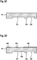
- Fig. 3C shows a partial sectional view of the first semiconductor substrate 101 from Fig. 3B with the first recess portion 231 and the second recess portion 232, which are formed by microstructuring, for example by trenches, in the first semiconductor substrate 101.
- the first recess section 231 and the second recess section 232 have a second recess depth, which is greater than the first recess depth of the third recess section 233.
- Fig. 3D shows a sectional view of the first semiconductor substrate 101 Fig. 3C with the subsections of the at least one etch stop layer 240, which is applied to subregions of surfaces of the first semiconductor substrate 101, for example, by deposition and patterning.
- the at least one etch stop layer 240 comprises, for example, silicon nitride (Si 3 N 4 ).
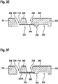
- Fig. 3E shows a sectional view of the first semiconductor substrate 101 Fig. 3D with the fourth recess portion 234 and the fifth recess portion 235, which are formed by etching in the first semiconductor substrate 101, for example.
- the fourth recess portion 234 and the fifth recess portion 235 are etched using the at least one etching stopper layer 240.
- the fourth recessed portion 234 and the fifth recessed portion 235 are formed in this embodiment by KOH etching.
- the fourth recess portion 234 and / or the fifth recess portion 235 may also be separated.
- a portion of the etching stopper layer 240 is disposed as an auxiliary membrane.
- the first recessed portion 231 is separated from the fifth recessed portion 235 by the portion of the etching stopper layer 240 and the auxiliary diaphragm, respectively.
- first recessed portion 231 and the fifth recessed portion 235 adjoin the portion of the etching stopper layer 240 and the auxiliary membrane, respectively.
- Fig. 3F shows a sectional view of the first semiconductor substrate 101 Fig. 3E with the first solid electrolyte layer 221A deposited on sides of the first recess portion 231 at the portion of the etching stopper layer 240 and the auxiliary membrane, respectively.
- the first solid electrolyte layer 221A is deposited, for example, by means of pulsed laser deposition (PLD), sputtering or the like.
- the first solid electrolyte layer 221A has, for example, an ion-conducting, yttrium-doped zirconium oxide or ZrO 2 ceramic (YSZ).
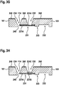
- Fig. 3G shows a sectional view of the first semiconductor substrate 101 Fig. 3F wherein the partial portion of the etch stop layer 240 and the auxiliary membrane are partially removed from the first solid electrolyte layer 221A, respectively. Specifically, the portion of the etching stopper layer 240 and the auxiliary membrane are removed from the first solid electrolyte layer 221A in a portion of the fifth recess portion 235.
- Fig. 3H shows a sectional view of the first semiconductor substrate 101 Fig. 3G with the first inner electrode 221B and the first outer electrode 221C deposited on the first solid electrolyte layer 221A.
- the first inner electrode 221B is disposed on the first solid electrolyte layer 221A side of the first recessed portion 231, and the first outer electrode 221C on the fifth recessed portion 235 side is disposed on the first solid electrolyte layer 221A.
- the first semiconductor substrate 101 shown corresponds to the first semiconductor substrate Fig. 2A ,
- FIGS. 4A to 4G show sectional views with regard to method steps of a production or with respect to production states of the second semiconductor substrate 102 Fig. 2B ,
- Fig. 4A shows a sectional view of the second semiconductor substrate 102 in an unprocessed state.
- the second semiconductor substrate 102 is formed of silicon, for example.
- Fig. 4B shows a sectional view of the second semiconductor substrate 102 from Fig. 4A with the sixth recessed portion 236 and the seventh recessed portion 237, which are formed by microstructuring such as trenches in the second semiconductor substrate 102.
- Fig. 4C shows a sectional view of the second semiconductor substrate 102 from Fig. 4B with the subsections of the at least one etch stop layer 240, which is applied to subregions of surfaces of the second semiconductor substrate 102, for example, by deposition and patterning.
- the at least one etch stop layer 240 comprises, for example, silicon nitride (Si 3 N 4 ).
- Fig. 4D shows a sectional view of the second semiconductor substrate 102 from Fig. 4C with the eighth recess portion 238 and the ninth recess portion 239, which are formed by etching in the second semiconductor substrate 102, for example.
- the eighth recess portion 238 and the ninth recess portion 239 are etched using the at least one etching stopper layer 240.
- the eighth recess portion 238 and the ninth recess portion 239 are formed by KOH etching.
- a partial portion of the etching stopper layer 240 is disposed as an auxiliary membrane.
- the sixth recessed portion 236 and the eighth recessed portion 238 and the seventh recessed portion 237 and the ninth recessed portion 239 are separated from each other by the respective portion of the etching stopper layer 240 and the respective auxiliary diaphragm.
- the sixth recess portion 236 and the eighth recess portion 238 adjoin a portion of the etch stop layer 240 and an auxiliary diaphragm, respectively
- the seventh recess portion 237 and the ninth recess portion 239 adjoin another portion of the etch stop layer 240 and another auxiliary diaphragm, respectively.
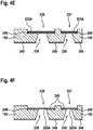
- Fig. 4E shows a sectional view of the second semiconductor substrate 102 from Fig. 4D with the second solid electrolyte layer 222A deposited on sides of the sixth recess portion 236 at the portion of the etch stop layer 240 and the auxiliary membrane, and the third solid electrolyte layer 223A on the side of the seventh recess portion 237 on the other portion of the etch stop layer 240 and the others, respectively Auxiliary membrane is deposited.
- the second solid electrolyte layer 222A and the third solid electrolyte layer 223A are deposited, for example, by pulsed laser deposition (PLD), sputtering, or the like.
- the second solid electrolyte layer 222A and the third solid electrolyte layer 223A have, for example, an ion-conducting, yttrium-doped zirconium oxide or ZrO 2 ceramic (YSZ).
- Fig. 4F shows a sectional view of the second semiconductor substrate 102 from Fig. 4E wherein the portions of the etch stop layer 240 and the auxiliary membranes of the second solid electrolyte layer 222A and the third solid electrolyte layer 223A are partially removed. Specifically, the portion of the etching stopper layer 240 and the auxiliary membrane are removed from the second solid electrolyte layer 222A in a region of the eighth recessed portion 238, and the further portion of the etch stop layer 240 and the further auxiliary membrane in a portion of the ninth recess portion 239 of the third solid electrolyte layer 223A is removed.
- Fig. 4G shows a sectional view of the second semiconductor substrate 102 from Fig. 4F with the second inner electrode 222B and the second outer electrode 222C deposited on the second solid electrolyte layer 222A, and the third inner electrode 223B and the third outer electrode 223C deposited on the third solid electrolyte layer 223A.
- the second inner electrode 222B is disposed on the sixth solid recessed portion 236 side of the second solid electrolyte layer 222A
- the second outer electrode 222C is disposed on the 8th recessed portion 238 side of the second solid electrolyte layer 222A.
- the third inner electrode 223B is disposed on sides of the seventh recess portion 237 on the third solid electrolyte layer 223A with the third outer electrode 223C on sides of the ninth recess portion 239 the third solid electrolyte layer 223A is arranged.
- This in Fig. 4G shown second semiconductor substrate 102 here corresponds to the second semiconductor substrate Fig. 2B ,
- a gas sensor device 100 embodied as a thin-film NOx sensor according to an embodiment of the present invention is shown and described.
- the semiconductor-based thin-film NOx sensor or the gas sensor device 100 is constructed here from two semiconductor substrates 101 and 102 or microchips. Manufacturing and operation of such a gas sensor device 100 will be described below with reference to FIGS FIGS. 1 to 4G explained.
- suitable recessed portions 231 to 239 or cavities are prepared.
- the semiconductor substrates 101 and 102 there may be used, for example, silicon (Si), silicon carbide (SiC), gallium arsenide (GaAs), gallium nitride (GaN), and other materials processable by semiconductor technology processes.
- a sensor function is based on an ion-conducting, yttrium-doped ZrO 2 ceramic (YSZ) for the solid electrolyte layers 221A, 222A and 223A, which are deposited as a thin layer.
- Electrode materials for the electrodes 221B, 221C, 222B, 222C, 223B, and 223C include, for example, compounds of Pt, Rh, Au, Re, Hf, Zr, etc., with deposition by, for example, sputtering or wet chemical deposition methods.
- Both semiconductor substrates 101 and 102 are formed by wafer bonding, e.g. B. Si direct bonding, put together.
- the adjustment chamber 111, the detection chamber 112, and the diffusion portion 113 are generated.
- a thin gap as the diffusion portion 113 between the adjustment chamber 111 and the detection chamber 112 functions as a diffusion barrier.
- the eighth recess portion 238 and the ninth recess portion 239 may be configured as reference air chambers.
- Such reference air chambers can similar to a conventional lambda probe as a real reference, ie be designed with reference air duct, or closed as a pumped reference.
- the electrodes arranged within the chambers 111 and 112, i. H. the internal electrodes 221B, 222B and 223B are connected together, so that only one common signal line for electrically contacting the same is needed.
- the electrodes disposed outside the chambers 111 and 112, i. H. the outer electrodes 221C, 222C and 223C are each connected with a dedicated line. In total, therefore, only four signal lines result for the electrodes of the gas sensor device 100. In addition, two further signal lines can come, which are used for controlling a heater or a tempering.
- the gas sensor device 100 can be heated as a whole or it can be heated by means of, for example, three parallel or serially connected diaphragm heater only the setting device 121, the determination device 122 and the detection device 123 designed as Nernst cells or pump cells.
- the gas sensor device 100 has geometric dimensions of, for example, about 3 millimeters by 3 millimeters by 1 millimeter.
- the measuring medium M or the gas to be measured via the inlet opening 114 and an etched opening in the first semiconductor substrate 101 in the adjustment chamber 111 passes.
- a Nernst voltage between the second inner electrode 222B and the second outer electrode 222C of Determining means 122 a currently present in the adjustment chamber 111 content of oxygen is to be measured as associated gas.
- oxygen can be pumped out of the adjustment chamber 111 and the adjustment chamber 111, respectively.
- the pumping voltage is regulated, for example, so that as constant as possible a low oxygen content in the adjustment chamber 111 is present.
- the z. B. formed from Pt-Rh-cermet due to their catalytic activity in the detection chamber 112 present nitrogen oxides are decomposed into nitrogen and oxygen and the present molecular oxygen is decomposed into atomic oxygen.
- the oxygen is removed from the detection chamber 112. Since a concentration of molecular oxygen as accompanying gas from the adjustment chamber 112 is set to a desired value and known, a concentration of the nitrogen oxides in the measurement medium M can be deduced based on the pumping current between the third inner electrode 223B and the third electrode 223C.
- FIG. 12 shows a flowchart of a method 500 according to an embodiment of the present invention.
- the method 500 is a method for producing a gas sensor device for detecting at least one gaseous analyte in a measurement medium.
- a gas sensor device such as the gas sensor device is made of FIGS. 1 to 4G produced. In particular, this results in at least a subset of in FIGS. 3A to 4G illustrated manufacturing conditions when the method 500 is executed.
- a first semiconductor substrate and a second semiconductor substrate are processed using at least one separation process and at least one coating process to produce recess portions, solid electrolyte layers, and electrodes in the first semiconductor substrate and the second semiconductor substrate.
- the first semiconductor substrate and the second semiconductor substrate are joined to define between the first semiconductor substrate and the second semiconductor substrate an adjustment chamber for adjusting a gas composition of the measurement medium, a detection chamber for detecting the gaseous analyte, and a diffusion section for controlling diffusion of the measurement medium the adjustment chamber and the detection chamber to produce.
- FIG. 12 shows a flowchart of a method 600 according to one embodiment of the present invention.
- the method 600 is a method for detecting at least one gaseous analyte in a measurement medium.
- the method 600 is in conjunction with a gas sensor device such as the gas sensor device of the FIGS. 1 to 4G advantageous executable.
- a gas sensor device such as the gas sensor device becomes out of the FIGS. 1 to 4G provided.
- a content of an accompanying gas of the measuring medium in the adjusting chamber of the gas sensor device is determined.
- a gas composition of the measuring medium in the adjusting chamber is adjusted with respect to the accompanying gas.
- the gaseous analyte is detected in the measurement medium diffused into the detection chamber.
- a gas sensor device designed as a zirconia-based nitrogen oxide sensor which is embodied as a two-chamber system, is based inter alia on an oxygen ion conductivity of the ZrO 2 ceramic of the solid electrolyte layers.
- an oxygen concentration is controlled to a very constant, low value by means of selective pump and a measuring electrodes.
- the gas mixture of the measured medium enters the detection chamber.
- the nitrogen oxides contained in the gas mixture are decomposed.
- the released oxygen is pumped out together with the oxygen content set in the adjustment chamber.
- the resulting pumping current is directly proportional to the nitrogen oxide concentration in the measuring medium and thus serves as a sensor signal.
- an exemplary embodiment comprises a "and / or" link between a first feature and a second feature, then this is to be read so that the embodiment according to one embodiment, both the first feature and the second feature and according to another embodiment either only first feature or only the second feature.
Landscapes
- Chemical & Material Sciences (AREA)
- Life Sciences & Earth Sciences (AREA)
- Health & Medical Sciences (AREA)
- Physics & Mathematics (AREA)
- Chemical Kinetics & Catalysis (AREA)
- Electrochemistry (AREA)
- Molecular Biology (AREA)
- Analytical Chemistry (AREA)
- Biochemistry (AREA)
- General Health & Medical Sciences (AREA)
- General Physics & Mathematics (AREA)
- Immunology (AREA)
- Pathology (AREA)
- Investigating Or Analyzing Materials By The Use Of Fluid Adsorption Or Reactions (AREA)
Claims (9)
- Procédé (500) pour fabriquer un arrangement détecteur de gaz (100) destiné à détecter au moins une substance à analyser sous forme gazeuse dans un fluide de mesure (M), le procédé (500) comprenant les étapes suivantes :traitement (510) d'un premier substrat en semiconducteur (101) et d'un deuxième substrat en semiconducteur (102) en utilisant au moins un processus de séparation et au moins un processus de revêtement afin de produire des portions d'évidement (231, 232, 233, 234, 235, 236, 237, 238, 239), des couches d'électrolyte solide (221A, 222A, 223A) et des électrodes (221B, 221C, 222B, 222C, 223B, 223C) dans le premier substrat en semiconducteur (101) et le deuxième substrat en semiconducteur (102), dans l'étape (510) de traitement, un dispositif de réglage (121) pourvu d'une première couche d'électrolyte solide (221A) entre une première paire d'électrodes (221B, 221C) servant à régler une composition de gaz du fluide de mesure (M) du point de vue d'un gaz d'accompagnement, un dispositif de détermination (122) pourvu d'une deuxième couche d'électrolyte solide (222A) entre une deuxième paire d'électrodes (222B, 222C) servant à déterminer une teneur en le gaz d'accompagnement dans le fluide de mesure (M) et un dispositif de détection (123) pourvu d'une troisième couche d'électrolyte solide (223A) entre une troisième paire d'électrodes (223B, 223C) servant à détecter la substance à analyser sous forme gazeuse étant produits sur le premier substrat en semiconducteur (101) et/ou sur le deuxième substrat en semiconducteur (102), le dispositif de détermination (122), le dispositif de réglage (121) et le dispositif de détection (123) étant disposés de manière isolée galvaniquement les uns des autres, de sorte que dans un état assemblé du premier substrat en semiconducteur (101) et du deuxième substrat en semiconducteur (102), le dispositif de détermination (122) et le dispositif de réglage (121) sont façonnés en tant que portions de paroi d'une chambre de réglage (111) et le dispositif de détection (123) est façonné en tant qu'une portion de paroi d'une chambre de détection (112) ; etassemblage (520) du premier substrat en semiconducteur (101) et du deuxième substrat en semiconducteur (102) afin de produire entre le premier substrat en semiconducteur (101) et le deuxième substrat en semiconducteur (102) la chambre de réglage (111) servant à régler une composition de gaz du fluide de mesure (M), la chambre de détection (112) servant à détecter la substance à analyser sous forme gazeuse et une portion de diffusion (113) servant à commander une diffusion du fluide de mesure (M) entre la chambre de réglage (111) et la chambre de détection (112).
- Procédé (500) selon l'une de la revendication 1, caractérisé en ce que dans l'étape (510) de traitement, une ligne de signal électrique commune est raccordée aux électrodes (221B, 222B, 223B) qui sont disposées en faisant face à la chambre de réglage (111) et à la chambre de détection (112) et des lignes de signal électriques propres sont raccordées aux électrodes (221C, 222C, 223C) qui sont disposées opposées à la chambre de réglage (111) et à la chambre de détection (112).
- Procédé (500) selon l'une des revendications précédentes, caractérisé en ce que dans l'étape (510) de traitement, au moins un dispositif d'équilibrage de température destiné à équilibrer la température des couches d'électrolyte solide (221A, 222A, 223A) et/ou des électrodes (221B, 221C, 222B, 222C, 223B, 223C) est disposé dans une zone du premier substrat en semiconducteur (101) et/ou dans une zone du deuxième substrat en semiconducteur (102).
- Procédé (500) selon l'une des revendications précédentes, caractérisé en ce que dans l'étape (510) de traitement, un dispositif d'interprétation est intégré dans une zone du premier substrat en semiconducteur (101) et/ou dans une zone du deuxième substrat en semiconducteur (102).
- Arrangement détecteur de gaz (100) destiné à détecter au moins une substance à analyser sous forme gazeuse dans un fluide de mesure (M), l'arrangement détecteur de gaz (100) possédant les caractéristiques suivantes :
un premier substrat en semiconducteur (101) et un deuxième substrat en semiconducteur (102), lesquels possèdent des portions d'évidement (231, 232, 233, 234, 235, 236, 237, 238, 239), des couches d'électrolyte solide (221A, 222A, 223A) et des électrodes (221B, 221C, 222B, 222C, 223B, 223C) produites en utilisant au moins un processus de séparation et au moins un processus de revêtement, le premier substrat en semiconducteur (101) et le deuxième substrat en semiconducteur (102) étant assemblés, une chambre de réglage (111) servant à régler une composition de gaz du fluide de mesure (M), une chambre de détection (112) servant à détecter la substance à analyser sous forme gazeuse et une portion de diffusion (113) servant à commander une diffusion du fluide de mesure (M) entre la chambre de réglage (111) et la chambre de détection (112) étant disposées entre le premier substrat en semiconducteur (101) et le deuxième substrat en semiconducteur (102) à l'état assemblé, un dispositif de réglage (121) pourvu d'une première couche d'électrolyte solide (221A) entre une première paire d'électrodes (221B, 221C) servant à régler une composition de gaz du fluide de mesure (M) du point de vue d'un gaz d'accompagnement, un dispositif de détermination (122) pourvu d'une deuxième couche d'électrolyte solide (222A) entre une deuxième paire d'électrodes (222B, 222C) servant à déterminer une teneur en le gaz d'accompagnement dans le fluide de mesure (M) et un dispositif de détection (123) pourvu d'une troisième couche d'électrolyte solide (223A) entre une troisième paire d'électrodes (223B, 223C) servant à détecter la substance à analyser sous forme gazeuse étant produits sur le premier substrat en semiconducteur (101) et/ou sur le deuxième substrat en semiconducteur (102), le dispositif de détermination (122), le dispositif de réglage (121) et le dispositif de détection (123) étant disposés de manière isolée galvaniquement les uns des autres, de sorte que dans un état assemblé du premier substrat en semiconducteur (101) et du deuxième substrat en semiconducteur (102), le dispositif de détermination (122) et le dispositif de réglage (121) sont façonnés en tant que portions de paroi de la chambre de réglage (111) et le dispositif de détection (123) est façonné en tant qu'une portion de paroi de la chambre de détection (112). - Arrangement détecteur de gaz (100) selon la revendication 5, caractérisé en ce que le premier substrat en semiconducteur (101) possède une première portion d'évidement (231) pour la chambre de réglage (111), une deuxième portion d'évidement (232) pour la chambre de détection (112), une troisième portion d'évidement (233) pour la portion de diffusion (113) entre la première portion d'évidement (231) et la deuxième portion d'évidement (232), une quatrième portion d'évidement (234) pour une ouverture d'accès (114) vers la chambre de réglage (111) pour le fluide de mesure (M), un dispositif de réglage (121) pourvu d'une première couche d'électrolyte solide (221A) entre une première paire d'électrodes (221B, 221C) servant à régler une composition de gaz du fluide de mesure (M) du point de vue d'un gaz d'accompagnement, le dispositif de réglage (121) étant façonné en tant qu'une portion de paroi de la chambre de réglage (111) dans la première portion d'évidement (231), et une cinquième portion d'évidement (235) pour le dispositif de réglage (121), le deuxième substrat en semiconducteur (102) possédant une sixième portion d'évidement (236) pour la chambre de réglage (111), une septième portion d'évidement (237) pour la chambre de détection (112), un dispositif de détermination (122) pourvu d'une deuxième couche d'électrolyte solide (222A) entre une deuxième paire d'électrodes (222B, 222C) servant à déterminer une teneur en un gaz d'accompagnement dans le fluide de mesure (M), le dispositif de détermination (122) étant façonné en tant qu'une portion de paroi de la chambre de réglage (111) dans la sixième portion d'évidement (236), un dispositif de détection (123) pourvu d'une troisième couche d'électrolyte solide (223A) entre une troisième paire d'électrodes (223B, 223C) servant à détecter la substance à analyser sous forme gazeuse, le dispositif de détection (123) étant façonné en tant qu'une portion de paroi de la chambre de détection (112) dans la septième portion d'évidement (237), une huitième portion d'évidement (238) pour le dispositif de détermination (122) et une neuvième portion d'évidement (239) pour le dispositif de détection (123).
- Procédé (600) de détection d'au moins une substance à analyser sous forme gazeuse dans un fluide de mesure (M), le procédé (600) comprenant les étapes suivantes :fourniture (610) d'un arrangement détecteur de gaz (100) selon l'une des revendications 5 et 6 ;détermination (620) d'une teneur en un gaz d'accompagnement du fluide de mesure (M) dans la chambre de réglage (111) ;réglage (630) d'une composition de gaz du fluide de mesure (M) dans la chambre de réglage (111) du point de vue du gaz d'accompagnement ; etdétection (640) de la substance à analyser sous forme gazeuse dans le fluide de mesure (M) diffusé dans la chambre de détection (112).
- Programme informatique, comprenant des instructions qui, lors de l'exécution du programme par un ordinateur, amènent celui-ci à exécuter, commander et/ou mettre en oeuvre toutes les étapes d'un procédé (500 ; 600) selon l'une des revendications 1 à 4 ou 7.
- Support d'enregistrement lisible par machine sur lequel est enregistré un programme informatique selon la revendication 8.
Applications Claiming Priority (2)
| Application Number | Priority Date | Filing Date | Title |
|---|---|---|---|
| DE102014226804.4A DE102014226804A1 (de) | 2014-12-22 | 2014-12-22 | Verfahren zum Herstellen einer Gassensorvorrichtung zum Erfassen zumindest eines gasförmigen Analyten in einem Messmedium sowie Verfahren und Gassensorvorrichtung zum Erfassen zumindest eines gasförmigen Analyten in einem Messmedium |
| PCT/EP2015/078959 WO2016102183A1 (fr) | 2014-12-22 | 2015-12-08 | Procédé de fabrication d'un dispositif de détection de gaz pour détecter au moins un analyte gazeux dans un milieu de mesure ainsi que procédé et dispositif de détection d'au moins un analyte gazeux dans un milieu de mesure |
Publications (2)
| Publication Number | Publication Date |
|---|---|
| EP3237898A1 EP3237898A1 (fr) | 2017-11-01 |
| EP3237898B1 true EP3237898B1 (fr) | 2019-05-01 |
Family
ID=54838350
Family Applications (1)
| Application Number | Title | Priority Date | Filing Date |
|---|---|---|---|
| EP15807655.4A Not-in-force EP3237898B1 (fr) | 2014-12-22 | 2015-12-08 | Procédé pour la fabrication d'un dispositif detecteur de gaz pour détecter au moins un analyte gazeux dans un fluide de mesure, ainsi procédé et dispositif detecteur de gaz pour détecter au moins un analyte gazeux dans un fluide de mesure |
Country Status (4)
| Country | Link |
|---|---|
| EP (1) | EP3237898B1 (fr) |
| CN (1) | CN107250783B (fr) |
| DE (1) | DE102014226804A1 (fr) |
| WO (1) | WO2016102183A1 (fr) |
Families Citing this family (8)
| Publication number | Priority date | Publication date | Assignee | Title |
|---|---|---|---|---|
| DE102015223646A1 (de) * | 2015-11-30 | 2017-06-01 | Robert Bosch Gmbh | Sensorelement zum Erfassen wenigstens eines Parameters eines, insbesondere sauerstoffhaltigen, Messgases |
| DE102015223654A1 (de) * | 2015-11-30 | 2017-06-01 | Robert Bosch Gmbh | Sensorelement zur Erfassung mindestens einer Eigenschaft eines Messgases in einem Messgasraum |
| DE102015223700A1 (de) * | 2015-11-30 | 2017-06-01 | Robert Bosch Gmbh | Sensorelement, Sensorvorrichtung und Verfahren zur Erfassung mindestens einer Eigenschaft eines Gases in einem Messgasraum |
| DE102015223693A1 (de) * | 2015-11-30 | 2017-06-01 | Robert Bosch Gmbh | Feststoffelektrolyt-Sensoranordnung und Verfahren zum Herstellen einer Feststoffelektrolyt-Sensoranordnung |
| DE102015224958B4 (de) * | 2015-12-11 | 2017-09-28 | Robert Bosch Gmbh | Gassensor und Verfahren zur Herstellung eines Gassensors |
| DE102015225176A1 (de) * | 2015-12-15 | 2017-06-22 | Robert Bosch Gmbh | Mikromechanische Feststoffelektrolyt-Sensorvorrichtung |
| DE102016213933B4 (de) * | 2016-07-28 | 2023-01-26 | Robert Bosch Gmbh | Sensorelement zur Erfassung wenigstens einer Eigenschaft eines Messgases |
| CN118465003B (zh) * | 2024-05-23 | 2025-06-17 | 山东产研微纳与智能制造研究院有限公司 | 一种mems气体传感器装置及制备方法 |
Family Cites Families (7)
| Publication number | Priority date | Publication date | Assignee | Title |
|---|---|---|---|---|
| US4668374A (en) * | 1986-07-07 | 1987-05-26 | General Motors Corporation | Gas sensor and method of fabricating same |
| JP2011102797A (ja) * | 2009-10-15 | 2011-05-26 | Ngk Insulators Ltd | ガスセンサおよびセンサ素子の製造方法 |
| US9395324B2 (en) * | 2010-12-14 | 2016-07-19 | Utc Fire & Security Corporation | Thin film micromachined gas sensor |
| MY159118A (en) * | 2011-05-12 | 2016-12-15 | Mimos Bhd | A gas sensing system |
| DE102012201304A1 (de) * | 2012-01-31 | 2013-08-01 | Robert Bosch Gmbh | Mikromechanische Feststoffelektrolyt-Sensorvorrichtung und entsprechendes Herstellungsverfahren |
| EP2762864B1 (fr) * | 2013-01-31 | 2018-08-08 | Sensirion AG | Dispositif de capteur à membrane et son procédé de fabrication |
| DE102013206637A1 (de) * | 2013-04-15 | 2014-10-16 | Robert Bosch Gmbh | Verfahren zum Analysieren eines Gases |
-
2014
- 2014-12-22 DE DE102014226804.4A patent/DE102014226804A1/de not_active Withdrawn
-
2015
- 2015-12-08 WO PCT/EP2015/078959 patent/WO2016102183A1/fr not_active Ceased
- 2015-12-08 EP EP15807655.4A patent/EP3237898B1/fr not_active Not-in-force
- 2015-12-08 CN CN201580076605.1A patent/CN107250783B/zh not_active Expired - Fee Related
Non-Patent Citations (1)
| Title |
|---|
| None * |
Also Published As
| Publication number | Publication date |
|---|---|
| EP3237898A1 (fr) | 2017-11-01 |
| DE102014226804A1 (de) | 2016-06-23 |
| CN107250783A (zh) | 2017-10-13 |
| CN107250783B (zh) | 2020-06-02 |
| WO2016102183A1 (fr) | 2016-06-30 |
Similar Documents
| Publication | Publication Date | Title |
|---|---|---|
| EP3237898B1 (fr) | Procédé pour la fabrication d'un dispositif detecteur de gaz pour détecter au moins un analyte gazeux dans un fluide de mesure, ainsi procédé et dispositif detecteur de gaz pour détecter au moins un analyte gazeux dans un fluide de mesure | |
| EP1428017B1 (fr) | Detecteur micromecanique a conductivite thermique presentant un recouvrement poreux | |
| EP2363705B1 (fr) | Électrode de référence microfabriquée avec une jonction liquide | |
| DE69720288T2 (de) | Integrierter keramischer abgassensor | |
| WO2015158599A1 (fr) | Dispositif de détection d'un paramètre d'un gaz, procédé pour faire fonctionner un tel dispositif et système de mesure pour déterminer un paramètre d'un gaz | |
| DE112016003247T5 (de) | Kontinuierliches, kapazitätsgestütztes Überwachen von Flüssigkeitsströmen in einer mikrofluidischen Einheit | |
| DE102013204197A1 (de) | Mikroelektrochemischer Sensor und Verfahren zum Betreiben eines mikroelektrochemischen Sensors | |
| DE102014223778A1 (de) | Vorrichtung zum Erfassen zumindest eines gasförmigen Analyten und Verfahren zum Herstellen derselben | |
| DE102007043132A1 (de) | Biosensor und ein Verfahren zum Messen einer Konzentration eines Analyten in einem Medium | |
| DE102012206476A1 (de) | Verfahren zum Betrieb eines Sensorelements zur Erfassung eines Sauerstoffanteils eines Gases in einem Messgasraum | |
| DE102019130755A1 (de) | Sensorvorrichtung, Verfahren zum Herstellen einer Sensorvorrichtung und Sensorbaugruppe | |
| DE102016222243A1 (de) | Gassensor | |
| DE102013206637A1 (de) | Verfahren zum Analysieren eines Gases | |
| WO2018206191A1 (fr) | Procédé de détermination de la température d'un capteur de gaz à électrolyte solide | |
| DE102016200781A1 (de) | Verfahren zum Herstellen einer Porenvorrichtung für eine Analyse von Molekülen, mikrofluidisches System zum Analysieren von Molekülen, Steuergerät und Verfahren zum Analysieren von Molekülen | |
| DE10123803C1 (de) | Elektrochemische Messzelle | |
| EP3104170B1 (fr) | Procede de fabrication d'un dispositif de capteur micro-mecanique d'electrolyte solide | |
| EP3227673B1 (fr) | Dispositif permettant de détecter un gaz et procédé de fabrication dudit dispositif | |
| DE102015214387B4 (de) | Sensorelement zur Erfassung mindestens einer Eigenschaft eines Messgases in einem Messgasraum und Verfahren zur Herstellung desselben | |
| DE102015223693A1 (de) | Feststoffelektrolyt-Sensoranordnung und Verfahren zum Herstellen einer Feststoffelektrolyt-Sensoranordnung | |
| US20060223168A1 (en) | Integrated CMOS-compatible biochip | |
| DE102007027183A1 (de) | Verfahren und Schaltungsanordnung zum Betreiben eines Gassensors | |
| DE102015223642B4 (de) | Gassensor und Verfahren zur Herstellung eines Gassensors | |
| DE102012209388A1 (de) | Verfahren zum Herstellen eines Sensorelements zur Erfassung mindestens einer Eigenschaft eines Messgases in einem Messgasraum | |
| DE102016213933B4 (de) | Sensorelement zur Erfassung wenigstens einer Eigenschaft eines Messgases |
Legal Events
| Date | Code | Title | Description |
|---|---|---|---|
| STAA | Information on the status of an ep patent application or granted ep patent |
Free format text: STATUS: THE INTERNATIONAL PUBLICATION HAS BEEN MADE |
|
| PUAI | Public reference made under article 153(3) epc to a published international application that has entered the european phase |
Free format text: ORIGINAL CODE: 0009012 |
|
| STAA | Information on the status of an ep patent application or granted ep patent |
Free format text: STATUS: REQUEST FOR EXAMINATION WAS MADE |
|
| 17P | Request for examination filed |
Effective date: 20170724 |
|
| AK | Designated contracting states |
Kind code of ref document: A1 Designated state(s): AL AT BE BG CH CY CZ DE DK EE ES FI FR GB GR HR HU IE IS IT LI LT LU LV MC MK MT NL NO PL PT RO RS SE SI SK SM TR |
|
| AX | Request for extension of the european patent |
Extension state: BA ME |
|
| DAV | Request for validation of the european patent (deleted) | ||
| DAX | Request for extension of the european patent (deleted) | ||
| GRAP | Despatch of communication of intention to grant a patent |
Free format text: ORIGINAL CODE: EPIDOSNIGR1 |
|
| STAA | Information on the status of an ep patent application or granted ep patent |
Free format text: STATUS: GRANT OF PATENT IS INTENDED |
|
| INTG | Intention to grant announced |
Effective date: 20181203 |
|
| GRAS | Grant fee paid |
Free format text: ORIGINAL CODE: EPIDOSNIGR3 |
|
| GRAA | (expected) grant |
Free format text: ORIGINAL CODE: 0009210 |
|
| STAA | Information on the status of an ep patent application or granted ep patent |
Free format text: STATUS: THE PATENT HAS BEEN GRANTED |
|
| AK | Designated contracting states |
Kind code of ref document: B1 Designated state(s): AL AT BE BG CH CY CZ DE DK EE ES FI FR GB GR HR HU IE IS IT LI LT LU LV MC MK MT NL NO PL PT RO RS SE SI SK SM TR |
|
| REG | Reference to a national code |
Ref country code: GB Ref legal event code: FG4D Free format text: NOT ENGLISH |
|
| REG | Reference to a national code |
Ref country code: CH Ref legal event code: EP Ref country code: AT Ref legal event code: REF Ref document number: 1127614 Country of ref document: AT Kind code of ref document: T Effective date: 20190515 |
|
| REG | Reference to a national code |
Ref country code: DE Ref legal event code: R096 Ref document number: 502015008924 Country of ref document: DE |
|
| REG | Reference to a national code |
Ref country code: IE Ref legal event code: FG4D Free format text: LANGUAGE OF EP DOCUMENT: GERMAN |
|
| REG | Reference to a national code |
Ref country code: NL Ref legal event code: MP Effective date: 20190501 |
|
| REG | Reference to a national code |
Ref country code: LT Ref legal event code: MG4D |
|
| PG25 | Lapsed in a contracting state [announced via postgrant information from national office to epo] |
Ref country code: NO Free format text: LAPSE BECAUSE OF FAILURE TO SUBMIT A TRANSLATION OF THE DESCRIPTION OR TO PAY THE FEE WITHIN THE PRESCRIBED TIME-LIMIT Effective date: 20190801 Ref country code: PT Free format text: LAPSE BECAUSE OF FAILURE TO SUBMIT A TRANSLATION OF THE DESCRIPTION OR TO PAY THE FEE WITHIN THE PRESCRIBED TIME-LIMIT Effective date: 20190901 Ref country code: FI Free format text: LAPSE BECAUSE OF FAILURE TO SUBMIT A TRANSLATION OF THE DESCRIPTION OR TO PAY THE FEE WITHIN THE PRESCRIBED TIME-LIMIT Effective date: 20190501 Ref country code: SE Free format text: LAPSE BECAUSE OF FAILURE TO SUBMIT A TRANSLATION OF THE DESCRIPTION OR TO PAY THE FEE WITHIN THE PRESCRIBED TIME-LIMIT Effective date: 20190501 Ref country code: AL Free format text: LAPSE BECAUSE OF FAILURE TO SUBMIT A TRANSLATION OF THE DESCRIPTION OR TO PAY THE FEE WITHIN THE PRESCRIBED TIME-LIMIT Effective date: 20190501 Ref country code: NL Free format text: LAPSE BECAUSE OF FAILURE TO SUBMIT A TRANSLATION OF THE DESCRIPTION OR TO PAY THE FEE WITHIN THE PRESCRIBED TIME-LIMIT Effective date: 20190501 Ref country code: HR Free format text: LAPSE BECAUSE OF FAILURE TO SUBMIT A TRANSLATION OF THE DESCRIPTION OR TO PAY THE FEE WITHIN THE PRESCRIBED TIME-LIMIT Effective date: 20190501 Ref country code: ES Free format text: LAPSE BECAUSE OF FAILURE TO SUBMIT A TRANSLATION OF THE DESCRIPTION OR TO PAY THE FEE WITHIN THE PRESCRIBED TIME-LIMIT Effective date: 20190501 Ref country code: LT Free format text: LAPSE BECAUSE OF FAILURE TO SUBMIT A TRANSLATION OF THE DESCRIPTION OR TO PAY THE FEE WITHIN THE PRESCRIBED TIME-LIMIT Effective date: 20190501 |
|
| PG25 | Lapsed in a contracting state [announced via postgrant information from national office to epo] |
Ref country code: LV Free format text: LAPSE BECAUSE OF FAILURE TO SUBMIT A TRANSLATION OF THE DESCRIPTION OR TO PAY THE FEE WITHIN THE PRESCRIBED TIME-LIMIT Effective date: 20190501 Ref country code: RS Free format text: LAPSE BECAUSE OF FAILURE TO SUBMIT A TRANSLATION OF THE DESCRIPTION OR TO PAY THE FEE WITHIN THE PRESCRIBED TIME-LIMIT Effective date: 20190501 Ref country code: GR Free format text: LAPSE BECAUSE OF FAILURE TO SUBMIT A TRANSLATION OF THE DESCRIPTION OR TO PAY THE FEE WITHIN THE PRESCRIBED TIME-LIMIT Effective date: 20190802 Ref country code: BG Free format text: LAPSE BECAUSE OF FAILURE TO SUBMIT A TRANSLATION OF THE DESCRIPTION OR TO PAY THE FEE WITHIN THE PRESCRIBED TIME-LIMIT Effective date: 20190801 |
|
| PG25 | Lapsed in a contracting state [announced via postgrant information from national office to epo] |
Ref country code: IS Free format text: LAPSE BECAUSE OF FAILURE TO SUBMIT A TRANSLATION OF THE DESCRIPTION OR TO PAY THE FEE WITHIN THE PRESCRIBED TIME-LIMIT Effective date: 20190901 |
|
| PG25 | Lapsed in a contracting state [announced via postgrant information from national office to epo] |
Ref country code: CZ Free format text: LAPSE BECAUSE OF FAILURE TO SUBMIT A TRANSLATION OF THE DESCRIPTION OR TO PAY THE FEE WITHIN THE PRESCRIBED TIME-LIMIT Effective date: 20190501 Ref country code: RO Free format text: LAPSE BECAUSE OF FAILURE TO SUBMIT A TRANSLATION OF THE DESCRIPTION OR TO PAY THE FEE WITHIN THE PRESCRIBED TIME-LIMIT Effective date: 20190501 Ref country code: SK Free format text: LAPSE BECAUSE OF FAILURE TO SUBMIT A TRANSLATION OF THE DESCRIPTION OR TO PAY THE FEE WITHIN THE PRESCRIBED TIME-LIMIT Effective date: 20190501 Ref country code: DK Free format text: LAPSE BECAUSE OF FAILURE TO SUBMIT A TRANSLATION OF THE DESCRIPTION OR TO PAY THE FEE WITHIN THE PRESCRIBED TIME-LIMIT Effective date: 20190501 Ref country code: EE Free format text: LAPSE BECAUSE OF FAILURE TO SUBMIT A TRANSLATION OF THE DESCRIPTION OR TO PAY THE FEE WITHIN THE PRESCRIBED TIME-LIMIT Effective date: 20190501 |
|
| REG | Reference to a national code |
Ref country code: DE Ref legal event code: R097 Ref document number: 502015008924 Country of ref document: DE |
|
| PG25 | Lapsed in a contracting state [announced via postgrant information from national office to epo] |
Ref country code: IT Free format text: LAPSE BECAUSE OF FAILURE TO SUBMIT A TRANSLATION OF THE DESCRIPTION OR TO PAY THE FEE WITHIN THE PRESCRIBED TIME-LIMIT Effective date: 20190501 Ref country code: SM Free format text: LAPSE BECAUSE OF FAILURE TO SUBMIT A TRANSLATION OF THE DESCRIPTION OR TO PAY THE FEE WITHIN THE PRESCRIBED TIME-LIMIT Effective date: 20190501 |
|
| PLBE | No opposition filed within time limit |
Free format text: ORIGINAL CODE: 0009261 |
|
| STAA | Information on the status of an ep patent application or granted ep patent |
Free format text: STATUS: NO OPPOSITION FILED WITHIN TIME LIMIT |
|
| PG25 | Lapsed in a contracting state [announced via postgrant information from national office to epo] |
Ref country code: TR Free format text: LAPSE BECAUSE OF FAILURE TO SUBMIT A TRANSLATION OF THE DESCRIPTION OR TO PAY THE FEE WITHIN THE PRESCRIBED TIME-LIMIT Effective date: 20190501 |
|
| 26N | No opposition filed |
Effective date: 20200204 |
|
| PG25 | Lapsed in a contracting state [announced via postgrant information from national office to epo] |
Ref country code: PL Free format text: LAPSE BECAUSE OF FAILURE TO SUBMIT A TRANSLATION OF THE DESCRIPTION OR TO PAY THE FEE WITHIN THE PRESCRIBED TIME-LIMIT Effective date: 20190501 |
|
| PG25 | Lapsed in a contracting state [announced via postgrant information from national office to epo] |
Ref country code: SI Free format text: LAPSE BECAUSE OF FAILURE TO SUBMIT A TRANSLATION OF THE DESCRIPTION OR TO PAY THE FEE WITHIN THE PRESCRIBED TIME-LIMIT Effective date: 20190501 |
|
| REG | Reference to a national code |
Ref country code: CH Ref legal event code: PL |
|
| REG | Reference to a national code |
Ref country code: BE Ref legal event code: MM Effective date: 20191231 |
|
| PG25 | Lapsed in a contracting state [announced via postgrant information from national office to epo] |
Ref country code: MC Free format text: LAPSE BECAUSE OF FAILURE TO SUBMIT A TRANSLATION OF THE DESCRIPTION OR TO PAY THE FEE WITHIN THE PRESCRIBED TIME-LIMIT Effective date: 20190501 |
|
| PG25 | Lapsed in a contracting state [announced via postgrant information from national office to epo] |
Ref country code: LU Free format text: LAPSE BECAUSE OF NON-PAYMENT OF DUE FEES Effective date: 20191208 Ref country code: IE Free format text: LAPSE BECAUSE OF NON-PAYMENT OF DUE FEES Effective date: 20191208 |
|
| PG25 | Lapsed in a contracting state [announced via postgrant information from national office to epo] |
Ref country code: BE Free format text: LAPSE BECAUSE OF NON-PAYMENT OF DUE FEES Effective date: 20191231 Ref country code: CH Free format text: LAPSE BECAUSE OF NON-PAYMENT OF DUE FEES Effective date: 20191231 Ref country code: LI Free format text: LAPSE BECAUSE OF NON-PAYMENT OF DUE FEES Effective date: 20191231 |
|
| PG25 | Lapsed in a contracting state [announced via postgrant information from national office to epo] |
Ref country code: CY Free format text: LAPSE BECAUSE OF FAILURE TO SUBMIT A TRANSLATION OF THE DESCRIPTION OR TO PAY THE FEE WITHIN THE PRESCRIBED TIME-LIMIT Effective date: 20190501 |
|
| PGFP | Annual fee paid to national office [announced via postgrant information from national office to epo] |
Ref country code: DE Payment date: 20210217 Year of fee payment: 6 |
|
| PG25 | Lapsed in a contracting state [announced via postgrant information from national office to epo] |
Ref country code: MT Free format text: LAPSE BECAUSE OF FAILURE TO SUBMIT A TRANSLATION OF THE DESCRIPTION OR TO PAY THE FEE WITHIN THE PRESCRIBED TIME-LIMIT Effective date: 20190501 Ref country code: HU Free format text: LAPSE BECAUSE OF FAILURE TO SUBMIT A TRANSLATION OF THE DESCRIPTION OR TO PAY THE FEE WITHIN THE PRESCRIBED TIME-LIMIT; INVALID AB INITIO Effective date: 20151208 |
|
| PGFP | Annual fee paid to national office [announced via postgrant information from national office to epo] |
Ref country code: FR Payment date: 20211220 Year of fee payment: 7 Ref country code: GB Payment date: 20211222 Year of fee payment: 7 |
|
| REG | Reference to a national code |
Ref country code: AT Ref legal event code: MM01 Ref document number: 1127614 Country of ref document: AT Kind code of ref document: T Effective date: 20201208 |
|
| PG25 | Lapsed in a contracting state [announced via postgrant information from national office to epo] |
Ref country code: AT Free format text: LAPSE BECAUSE OF NON-PAYMENT OF DUE FEES Effective date: 20201208 |
|
| PG25 | Lapsed in a contracting state [announced via postgrant information from national office to epo] |
Ref country code: MK Free format text: LAPSE BECAUSE OF FAILURE TO SUBMIT A TRANSLATION OF THE DESCRIPTION OR TO PAY THE FEE WITHIN THE PRESCRIBED TIME-LIMIT Effective date: 20190501 |
|
| REG | Reference to a national code |
Ref country code: DE Ref legal event code: R119 Ref document number: 502015008924 Country of ref document: DE |
|
| PG25 | Lapsed in a contracting state [announced via postgrant information from national office to epo] |
Ref country code: DE Free format text: LAPSE BECAUSE OF NON-PAYMENT OF DUE FEES Effective date: 20220701 |
|
| GBPC | Gb: european patent ceased through non-payment of renewal fee |
Effective date: 20221208 |
|
| PG25 | Lapsed in a contracting state [announced via postgrant information from national office to epo] |
Ref country code: GB Free format text: LAPSE BECAUSE OF NON-PAYMENT OF DUE FEES Effective date: 20221208 |
|
| PG25 | Lapsed in a contracting state [announced via postgrant information from national office to epo] |
Ref country code: FR Free format text: LAPSE BECAUSE OF NON-PAYMENT OF DUE FEES Effective date: 20221231 |