EP3238286B1 - Matériaux pour dispositifs électroniques - Google Patents
Matériaux pour dispositifs électroniques Download PDFInfo
- Publication number
- EP3238286B1 EP3238286B1 EP15805398.3A EP15805398A EP3238286B1 EP 3238286 B1 EP3238286 B1 EP 3238286B1 EP 15805398 A EP15805398 A EP 15805398A EP 3238286 B1 EP3238286 B1 EP 3238286B1
- Authority
- EP
- European Patent Office
- Prior art keywords
- formula
- group
- aromatic ring
- substituted
- groups
- Prior art date
- Legal status (The legal status is an assumption and is not a legal conclusion. Google has not performed a legal analysis and makes no representation as to the accuracy of the status listed.)
- Active
Links
Classifications
-
- H—ELECTRICITY
- H10—SEMICONDUCTOR DEVICES; ELECTRIC SOLID-STATE DEVICES NOT OTHERWISE PROVIDED FOR
- H10K—ORGANIC ELECTRIC SOLID-STATE DEVICES
- H10K85/00—Organic materials used in the body or electrodes of devices covered by this subclass
- H10K85/60—Organic compounds having low molecular weight
- H10K85/615—Polycyclic condensed aromatic hydrocarbons, e.g. anthracene
- H10K85/626—Polycyclic condensed aromatic hydrocarbons, e.g. anthracene containing more than one polycyclic condensed aromatic rings, e.g. bis-anthracene
-
- H—ELECTRICITY
- H10—SEMICONDUCTOR DEVICES; ELECTRIC SOLID-STATE DEVICES NOT OTHERWISE PROVIDED FOR
- H10K—ORGANIC ELECTRIC SOLID-STATE DEVICES
- H10K85/00—Organic materials used in the body or electrodes of devices covered by this subclass
- H10K85/60—Organic compounds having low molecular weight
- H10K85/631—Amine compounds having at least two aryl rest on at least one amine-nitrogen atom, e.g. triphenylamine
- H10K85/636—Amine compounds having at least two aryl rest on at least one amine-nitrogen atom, e.g. triphenylamine comprising heteroaromatic hydrocarbons as substituents on the nitrogen atom
-
- H—ELECTRICITY
- H10—SEMICONDUCTOR DEVICES; ELECTRIC SOLID-STATE DEVICES NOT OTHERWISE PROVIDED FOR
- H10K—ORGANIC ELECTRIC SOLID-STATE DEVICES
- H10K50/00—Organic light-emitting devices
- H10K50/10—OLEDs or polymer light-emitting diodes [PLED]
- H10K50/14—Carrier transporting layers
- H10K50/15—Hole transporting layers
-
- H—ELECTRICITY
- H10—SEMICONDUCTOR DEVICES; ELECTRIC SOLID-STATE DEVICES NOT OTHERWISE PROVIDED FOR
- H10K—ORGANIC ELECTRIC SOLID-STATE DEVICES
- H10K85/00—Organic materials used in the body or electrodes of devices covered by this subclass
- H10K85/60—Organic compounds having low molecular weight
- H10K85/631—Amine compounds having at least two aryl rest on at least one amine-nitrogen atom, e.g. triphenylamine
-
- H—ELECTRICITY
- H10—SEMICONDUCTOR DEVICES; ELECTRIC SOLID-STATE DEVICES NOT OTHERWISE PROVIDED FOR
- H10K—ORGANIC ELECTRIC SOLID-STATE DEVICES
- H10K85/00—Organic materials used in the body or electrodes of devices covered by this subclass
- H10K85/60—Organic compounds having low molecular weight
- H10K85/631—Amine compounds having at least two aryl rest on at least one amine-nitrogen atom, e.g. triphenylamine
- H10K85/633—Amine compounds having at least two aryl rest on at least one amine-nitrogen atom, e.g. triphenylamine comprising polycyclic condensed aromatic hydrocarbons as substituents on the nitrogen atom
-
- H—ELECTRICITY
- H10—SEMICONDUCTOR DEVICES; ELECTRIC SOLID-STATE DEVICES NOT OTHERWISE PROVIDED FOR
- H10K—ORGANIC ELECTRIC SOLID-STATE DEVICES
- H10K85/00—Organic materials used in the body or electrodes of devices covered by this subclass
- H10K85/60—Organic compounds having low molecular weight
- H10K85/649—Aromatic compounds comprising a hetero atom
- H10K85/657—Polycyclic condensed heteroaromatic hydrocarbons
-
- H—ELECTRICITY
- H10—SEMICONDUCTOR DEVICES; ELECTRIC SOLID-STATE DEVICES NOT OTHERWISE PROVIDED FOR
- H10K—ORGANIC ELECTRIC SOLID-STATE DEVICES
- H10K85/00—Organic materials used in the body or electrodes of devices covered by this subclass
- H10K85/60—Organic compounds having low molecular weight
- H10K85/649—Aromatic compounds comprising a hetero atom
- H10K85/657—Polycyclic condensed heteroaromatic hydrocarbons
- H10K85/6572—Polycyclic condensed heteroaromatic hydrocarbons comprising only nitrogen in the heteroaromatic polycondensed ring system, e.g. phenanthroline or carbazole
-
- H—ELECTRICITY
- H10—SEMICONDUCTOR DEVICES; ELECTRIC SOLID-STATE DEVICES NOT OTHERWISE PROVIDED FOR
- H10K—ORGANIC ELECTRIC SOLID-STATE DEVICES
- H10K85/00—Organic materials used in the body or electrodes of devices covered by this subclass
- H10K85/60—Organic compounds having low molecular weight
- H10K85/649—Aromatic compounds comprising a hetero atom
- H10K85/657—Polycyclic condensed heteroaromatic hydrocarbons
- H10K85/6574—Polycyclic condensed heteroaromatic hydrocarbons comprising only oxygen in the heteroaromatic polycondensed ring system, e.g. cumarine dyes
-
- H—ELECTRICITY
- H10—SEMICONDUCTOR DEVICES; ELECTRIC SOLID-STATE DEVICES NOT OTHERWISE PROVIDED FOR
- H10K—ORGANIC ELECTRIC SOLID-STATE DEVICES
- H10K85/00—Organic materials used in the body or electrodes of devices covered by this subclass
- H10K85/60—Organic compounds having low molecular weight
- H10K85/649—Aromatic compounds comprising a hetero atom
- H10K85/657—Polycyclic condensed heteroaromatic hydrocarbons
- H10K85/6576—Polycyclic condensed heteroaromatic hydrocarbons comprising only sulfur in the heteroaromatic polycondensed ring system, e.g. benzothiophene
-
- H—ELECTRICITY
- H10—SEMICONDUCTOR DEVICES; ELECTRIC SOLID-STATE DEVICES NOT OTHERWISE PROVIDED FOR
- H10K—ORGANIC ELECTRIC SOLID-STATE DEVICES
- H10K10/00—Organic devices specially adapted for rectifying, amplifying, oscillating or switching; Organic capacitors or resistors having potential barriers
- H10K10/40—Organic transistors
- H10K10/46—Field-effect transistors, e.g. organic thin-film transistors [OTFT]
- H10K10/462—Insulated gate field-effect transistors [IGFETs]
-
- H—ELECTRICITY
- H10—SEMICONDUCTOR DEVICES; ELECTRIC SOLID-STATE DEVICES NOT OTHERWISE PROVIDED FOR
- H10K—ORGANIC ELECTRIC SOLID-STATE DEVICES
- H10K2101/00—Properties of the organic materials covered by group H10K85/00
- H10K2101/10—Triplet emission
-
- H—ELECTRICITY
- H10—SEMICONDUCTOR DEVICES; ELECTRIC SOLID-STATE DEVICES NOT OTHERWISE PROVIDED FOR
- H10K—ORGANIC ELECTRIC SOLID-STATE DEVICES
- H10K30/00—Organic devices sensitive to infrared radiation, light, electromagnetic radiation of shorter wavelength or corpuscular radiation
-
- H—ELECTRICITY
- H10—SEMICONDUCTOR DEVICES; ELECTRIC SOLID-STATE DEVICES NOT OTHERWISE PROVIDED FOR
- H10K—ORGANIC ELECTRIC SOLID-STATE DEVICES
- H10K50/00—Organic light-emitting devices
- H10K50/10—OLEDs or polymer light-emitting diodes [PLED]
- H10K50/11—OLEDs or polymer light-emitting diodes [PLED] characterised by the electroluminescent [EL] layers
-
- H—ELECTRICITY
- H10—SEMICONDUCTOR DEVICES; ELECTRIC SOLID-STATE DEVICES NOT OTHERWISE PROVIDED FOR
- H10K—ORGANIC ELECTRIC SOLID-STATE DEVICES
- H10K50/00—Organic light-emitting devices
- H10K50/10—OLEDs or polymer light-emitting diodes [PLED]
- H10K50/14—Carrier transporting layers
- H10K50/15—Hole transporting layers
- H10K50/155—Hole transporting layers comprising dopants
-
- Y—GENERAL TAGGING OF NEW TECHNOLOGICAL DEVELOPMENTS; GENERAL TAGGING OF CROSS-SECTIONAL TECHNOLOGIES SPANNING OVER SEVERAL SECTIONS OF THE IPC; TECHNICAL SUBJECTS COVERED BY FORMER USPC CROSS-REFERENCE ART COLLECTIONS [XRACs] AND DIGESTS
- Y02—TECHNOLOGIES OR APPLICATIONS FOR MITIGATION OR ADAPTATION AGAINST CLIMATE CHANGE
- Y02E—REDUCTION OF GREENHOUSE GAS [GHG] EMISSIONS, RELATED TO ENERGY GENERATION, TRANSMISSION OR DISTRIBUTION
- Y02E10/00—Energy generation through renewable energy sources
- Y02E10/50—Photovoltaic [PV] energy
- Y02E10/549—Organic PV cells
Definitions
- the present application relates to a spirobifluorene derivative of a formula (I) defined below, which is suitable for use in electronic devices, in particular organic electroluminescence devices (OLEDs).
- OLEDs organic electroluminescence devices
- Organic electronic devices in the sense of this application are understood to mean so-called organic electronic devices, which contain organic semiconductor materials as functional materials. In particular, this refers to OLEDs.
- OLEDs in which organic compounds are used as functional materials are used as functional materials are, for example, in US 4539507 , US 5151629 , EP 0676461 and WO 98/27136 described.
- OLEDs refers to electronic devices that have one or more layers containing organic compounds and emit light when electrical voltage is applied.
- Layers with a hole-transporting function such as hole-injecting layers, hole-transporting layers, electron blocking layers and also emitting layers, have a major influence on the performance data of electronic devices. New materials with hole-transporting properties are continually being sought for use in these layers.
- triarylamines As materials with hole-transporting properties in these layers.
- the triarylamines can be mono-triarylamines, such as in JP 1995/053955 , WO 2006/123667 and JP 2010/222268 described, or Represent bis- or other oligoamines, such as in US 7504163 or US 2005/0184657 described.
- the compounds found have one or more properties selected from very good hole-conducting properties, very good electron-blocking properties, high glass transition temperature, high oxidation stability, good solubility and high temperature stability.
- very good device performance data in particular very good service life and quantum efficiency of the devices, are observed.
- the groups in square brackets with index i, k, m, n and p can generally, including for the following structures, only be bound to the spirobifluorene skeleton in positions that are shown unsubstituted. In particular, they cannot be bound in positions that carry a residue R 0 .
- An aryl group in the context of this invention contains 6 to 40 aromatic ring atoms, none of which represents a heteroatom.
- an aryl group is understood to mean either a simple aromatic cycle, i.e. benzene, or a fused aromatic polycycle, for example naphthalene, phenanthrene or anthracene.
- a fused aromatic polycycle consists of two or more simple aromatic cycles condensed together. Condensation between cycles means that the cycles share at least one edge with each other.
- a heteroaryl group in the context of this invention contains 5 to 40 aromatic ring atoms, at least one of which represents a heteroatom.
- the heteroatoms of the heteroaryl group are preferably selected from N, O and S.
- a heteroaryl group in the context of this invention is understood to mean either a simple heteroaromatic cycle, for example pyridine, pyrimidine or thiophene, or a fused heteroaromatic polycycle, for example quinoline or carbazole.
- a fused heteroaromatic polycycle consists of two or more simple heteroaromatic cycles condensed together. Condensation between cycles means that the cycles share at least one edge with each other.
- An aryl or heteroaryl group which can be substituted with the above-mentioned radicals and which can be linked via any position on the aromatic or heteroaromatic, is understood to mean, in particular, groups which are derived from benzene, naphthalene, anthracene, phenanthrene, pyrene, Dihydropyrene, chrysene, perylene, triphenylene, fluoranthene, benzanthracene, benzophenanthrene, tetracene, pentacene, benzopyrene, furan, benzofuran, isobenzofuran, dibenzofuran, thiophene, benzothiophene, isobenzothiophene, dibenzothiophene, pyrrole, indole, isoindole, carbazole, pyridine, quinoline, isochine olin, Acridine, phenanthridine, benzo-5,6-quinoline, be
- An aromatic ring system in the sense of this invention contains 6 to 40 carbon atoms in the ring system and does not include any heteroatoms as aromatic ring atoms.
- An aromatic ring system in the sense of this invention therefore contains no heteroaryl groups.
- an aromatic ring system is to be understood as meaning a system which does not necessarily only contain aryl groups, but in which several aryl groups are also linked by a single bond or by a non-aromatic unit, such as one or more optionally substituted C-, Si- , N, O or S atoms, can be connected.
- the non-aromatic unit preferably comprises less than 10% of the atoms other than H, based on the total number of atoms other than H in the system.
- systems such as 9,9'-spirobifluorene, 9,9'-diarylfluorene, triarylamine, diaryl ether and stilbene should also be understood as aromatic ring systems within the meaning of this invention, and likewise Systems in which two or more aryl groups are linked, for example, by a linear or cyclic alkyl, alkenyl or alkynyl group or by a silyl group. Furthermore, systems in which two or more aryl groups are linked to one another via single bonds are also understood to be aromatic ring systems in the sense of this invention, such as systems such as biphenyl and terphenyl.
- a heteroaromatic ring system in the sense of this invention contains 5 to 40 aromatic ring atoms, of which at least one is a heteroatom.
- the heteroatoms of the heteroaromatic ring system are preferably selected from N, O and/or S.
- a heteroaromatic ring system corresponds to the above-mentioned definition of an aromatic ring system, but has at least one heteroatom as one of the aromatic ring atoms. This differs from an aromatic ring system in the sense of the definition of the present application, which according to this definition cannot contain a heteroatom as an aromatic ring atom.
- An aromatic ring system with 6 to 40 aromatic ring atoms or a heteroaromatic ring system with 5 to 40 aromatic ring atoms is understood to mean in particular groups that are derived from the groups mentioned above under aryl groups and heteroaryl groups as well as from biphenyl, terphenyl, quaterphenyl, fluorene, spirobifluorene, Dihydrophenanthrene, dihydropyrene, tetrahydropyrene, indenofluorene, truxene, isotruxene, spirotruxene, spiroisotruxene, indenocarbazole, or combinations of these groups.
- a straight-chain alkyl group with 1 to 20 carbon atoms or a branched or cyclic alkyl group with 3 to 20 carbon atoms or an alkenyl or alkynyl group with 2 to 40 carbon atoms in which also individual H atoms or CH 2 groups can be substituted by the groups mentioned above in the definition of the radicals, preferably the radicals methyl, ethyl, n-propyl, i-propyl, n-butyl, i-butyl, s-butyl, t -Butyl, 2-methylbutyl, n-pentyl, s-pentyl, cyclopentyl, neo-pentyl, n-hexyl, cyclohexyl, neo-hexyl, n-heptyl, cycloheptyl, n-octyl, cyclooctyl, 2-
- alkoxy or thioalkyl group with 1 to 20 carbon atoms in which individual H atoms or CH 2 groups can also be substituted by the groups mentioned above in the definition of the radicals, preference is given to methoxy, trifluoromethoxy, ethoxy, n- Propoxy, i-Propoxy, n-Butoxy, i-Butoxy, s-Butoxy, t-Butoxy, n-Pentoxy, s-Pentoxy, 2-Methylbutoxy, n-Hexoxy, Cyclohexyloxy, n-Heptoxy, Cycloheptyloxy, n-Octyloxy, Cyclooctyloxy, 2-Ethylhexyloxy, Pentafluorethoxy, 2,2,2-Trifluorethoxy, Methylthio, Ethylthio, n-Propylthio, i-Propylthio, n-Butylthio, i
- the wording that two or more radicals can form a ring together is intended to mean, among other things, that the two radicals are linked to one another by a chemical bond.
- the above-mentioned formulation should also be understood to mean that in the event that one of the two radicals represents hydrogen, the second radical binds to the position to which the hydrogen atom was bonded, forming a ring.
- A is a group of formula (A-1) or (A-3), particularly preferably a group of formula (A-1).
- Ar 1 is chosen the same or differently in each occurrence from a single bond or a divalent group derived from benzene, biphenyl, terphenyl, fluorene, spirobifluorene, indenofluorene, carbazole, dibenzofuran, dibenzothiophene, or one optionally substituted with radicals R 2 Combination of two or more of these groups, but not more than 30 aromatic ring atoms may be present in Ar 1 .
- Groups Ar 1 are preferably selected from groups of the following formulas: where the dashed bonds represent the bonds to the rest of the compound and the groups at the free positions can be substituted by one or more radicals R 2 , but are preferably unsubstituted at the free positions.
- R 2 in the groups of the formulas (Ar 1 -23) and (Ar 1 -24) preferably represents, identically or differently, an alkyl group with 1 to 10 carbon atoms, in particular methyl, or a phenyl group which has one or several radicals R 3 can be substituted and is preferably unsubstituted.
- Two alkyl groups R 2 can also form a ring to form a spiro group, preferably a cyclohexyl ring or a cyclopentyl ring.
- Ar 2 is chosen identically or differently for each occurrence from an aromatic or heteroaromatic ring system with 6 to 25 aromatic ring atoms, which can be substituted with one or more R 2 radicals.
- Particularly preferred are phenyl, biphenyl, terphenyl, fluorenyl, spirobifluorenyl, indenofluorenyl, naphthyl, phenanthrenyl, furanyl, benzofuranyl, dibenzofuranyl, thiophenyl, benzothiophenyl, dibenzothiophenyl, carbazolyl, indolocarbazolyl and indenocarbazolyl, which can each be substituted with one or more R 2 radicals.
- Groups Ar 2 are preferably the same or different each time they occur, selected from groups of the following formulas: Ar 2 -1 Ar 2 -2 Ar 2 -3 Ar 2 -4 Ar 2 -5 Ar 2 -6 Ar 2 -7 Ar 2 -8 Ar 2 -9 Ar 2 -10 Ar 2 -11 Ar 2 -12 Ar 2 -13 Ar 2 -14 Ar 2 -15 Ar 2 -16 Ar 2 -17 Ar 2 -18 Ar 2 -19 Ar 2 -20 Ar 2 -21 Ar 2 -22 Ar 2 -23 Ar 2 -24 Ar 2 -25 Ar 2 -26 Ar 2 -27 Ar 2 -28 Ar 2 -29 Ar 2 -30 Ar 2 -31 Ar 2 -32 Ar 2 -33 Ar 2 -34 Ar 2 -35 Ar 2 -36 Ar 2 -37 Ar 2 -38 Ar 2 -39 Ar 2 -40 Ar 2 -41 Ar 2 -42 Ar 2 -43 Ar 2 -44 Ar 2 -45 Ar 2 -46 Ar 2 -47 Ar 2 -48 Ar 2 -49 Ar 2 -50 Ar 2 -51 Ar
- R 2 is in the groups of the formulas (Ar 2 -68) to (Ar 2 -82), (Ar 2 -85) to (Ar 2 -87), (Ar 2 -129) and (Ar 2 -130) preferably the same or different for an alkyl group with 1 to 10 carbon atoms, in particular for methyl, or a phenyl group, which can be substituted with one or more radicals R 3 and is preferably unsubstituted.
- Two alkyl groups R 2 can also form a ring to form a spiro group, preferably a cyclohexyl ring or a cyclopentyl ring.
- R 1 and R 2 are particularly preferably identical or different in each occurrence of H, D, F, CN, a straight-chain alkyl group with 1 to 10 carbon atoms or a branched or cyclic alkyl group with 3 to 10 carbon atoms, or an aromatic or heteroaromatic ring system with 6 to 25 aromatic ring atoms, where the alkyl and alkoxy groups mentioned and the aromatic or heteroaromatic ring systems mentioned can each be substituted with one or more radicals R 3 .
- R 1 and R 2 are identical or different in each occurrence of H, F, CN, methyl, tert-butyl, phenyl, biphenyl, dibenzofuran, dibenzothiophene or carbazole.
- R 3 is particularly preferably identical or different in each occurrence of H, D, F, CN, N(R 4 ) 2 , a straight-chain alkyl group with 1 to 10 carbon atoms or a branched or cyclic alkyl group with 3 to 10 carbon atoms, or an aromatic or heteroaromatic ring system with 6 to 25 aromatic ring atoms, said alkyl and alkoxy groups and the aromatic or heteroaromatic ring systems mentioned can each be substituted with one or more radicals R 4 .
- p is equal to 1. In this case, it is further preferred that all other indices k, i, m and n are equal to 0.
- k is 1. In this case, it is further preferred that all other indices i, m, n and p are equal to 0.
- the sum of the indices i, k, m, n and p is equal to 1 or 2, particularly preferably equal to 1.
- the group Y is S and the group Z is O, S or a single bond.
- the group Y is S and the group Z is a single bond.
- Preferred embodiments of the compounds of formula (I) correspond to the following formulas: Formula (I-1) Formula (I-2) Formula (I-3) Formula (I-4) Formula (I-5) Formula (I-6) Formula (I-7) Formula (I-8) Formula (I-9) Formula (I-10) Formula (I-11) Formula (I-12) Formula (I-13) Formula (I-14) Formula (I-15) Formula (I-16) Formula (I-17) Formula (I-18) Formula (I-19) Formula (I-20) Formula (I-21) Formula (I-22) Formula (I-23) Formula (I-24) where the symbols appearing are as defined above, and the compounds can be substituted with radicals R 1 at positions shown unsubstituted.
- R 0 is preferably equal to S
- the group Z is O, S or a single bond
- R 0 is H.
- Formulas are particularly preferred among the formulas (I-1), (I-3), (I-5), (I-7), (I-9) and (I-11).
- Formula (I-1A) Formula (I-1B) Formula (I-3A) Formula (I-3B) Formula (I-5A) Formula (I-5B) Formula (I-7A) Formula (I-7B) Formula (I-9A) Formula (I-9B) Formula (I-11A) Formula (I-11B) where the symbols appearing are as defined above, and the compounds can be substituted with radicals R 1 at positions shown unsubstituted.
- R 0 , Ar 1 and A apply in particular to the formulas just mentioned.
- the group Y is preferably equal to S, and the group Z is O, S or a single bond; particularly preferably the group Y is S and the group Z is a single bond. Furthermore, it is particularly preferred for the above-mentioned formulas that R 0 is H.
- Schemes 1 to 8 show possible synthetic routes for producing the compounds according to the invention. They serve to explain the invention to those skilled in the art and are not to be interpreted in a restrictive manner. The person skilled in the art can, within the scope of his general specialist knowledge, modify the synthetic routes shown or develop other routes if this appears more advantageous.
- Scheme 3 shows a suitable synthesis for intermediates according to formulas (Z-3) and (Z-4).
- Scheme 7 According to an alternative process for producing the compounds according to the invention (Scheme 7), the procedure is analogous to Schemes 1 to 4, except that instead of the reactive group RG, a diarylamino group is present on the fluorenone derivative.
- Scheme 7 only the reaction analogous to Scheme 1 is shown.
- the processes according to Schemes 2 to 4 can also be modified, each by replacing the group RG with a corresponding diarylamino group.
- the reactive group is preferably a halogen atom, particularly preferably Br.
- the organometallic coupling reaction is preferably a Buchwald coupling or a Suzuki coupling.
- Suitable reactive leaving groups are, for example, bromine, iodine, chlorine, Boronic acids, boronic acid esters, amines, alkenyl or alkynyl groups with terminal CC double bonds or CC triple bonds, oxiranes, oxetanes, groups that undergo a cycloaddition, for example a 1,3-dipolar cycloaddition, such as dienes or azides, carboxylic acid derivatives, Alcohols and silanes.
- reactive leaving groups are, for example, bromine, iodine, chlorine, Boronic acids, boronic acid esters, amines, alkenyl or alkynyl groups with terminal CC double bonds or CC triple bonds, oxiranes, oxetanes, groups that undergo a cycloaddition, for example a 1,3-dipolar cycloaddition, such as dienes or azides, carboxylic acid derivatives, Alcohols and silanes.
- the invention therefore further provides oligomers, polymers or dendrimers containing one or more compounds according to formula (I), where the bond(s) to the polymer, oligomer or dendrimer are at any one, in formula (I) with R 0 , R 1 or R 2 substituted positions can be located.
- the compound is part of a side chain of the oligomer or polymer or part of the main chain.
- an oligomer is understood to mean a compound which is made up of at least three monomer units.
- a polymer is understood to mean a compound that is made up of at least ten monomer units.
- the polymers, oligomers or dendrimers according to the invention can be conjugated, partially conjugated or non-conjugated.
- the oligomers or polymers according to the invention can be linear, branched or dendritic.
- the units according to formula (I) can be linked to one another directly or they can be linked to one another via a bivalent group, for example via a substituted or unsubstituted alkylene group, via a heteroatom or via a divalent aromatic or heteroaromatic group.
- branched and dendritic structures for example, three or more units according to formula (I) can be linked via a trivalent or higher-valent group, for example via a trivalent or higher-valent aromatic or heteroaromatic group, to form a branched or dendritic oligomer or polymer.
- the monomers according to the invention are homopolymerized or copolymerized with other monomers.
- Suitable and preferred comonomers are selected from fluorenes (e.g. according to EP 842208 or WO 2000/22026 ), spirobifluorenes (e.g. according to EP 707020 , EP 894107 or WO 2006/061181 ), paraphenylenes (e.g. according to WO 1992/18552 ), carbazoles (e.g. according to WO 2004/070772 or WO 2004/113468 ), thiophenes (e.g. according to EP 1028136 ), dihydrophenanthrenes (e.g. according to WO 2005/014689 or WO 2007/006383 ), cis- and trans-indenofluorenes (e.g.
- the polymers, oligomers and dendrimers usually contain further units, for example emitting (fluorescent or phosphorescent) units, such as.
- emitting (fluorescent or phosphorescent) units such as.
- the polymers and oligomers according to the invention are generally produced by polymerizing one or more types of monomer, of which at least one monomer in the polymer leads to repeating units of the formula (I).
- Suitable polymerization reactions are known to those skilled in the art and are described in the literature.
- Particularly suitable and preferred polymerization reactions that lead to C-C or C-N bonds are SUZUKI polymerization, YAMAMOTO polymerization; STILLE polymerization; and the HARTWIG-BUCHWALD polymerization.
- Formulations of the compounds according to the invention are required for processing the compounds according to the invention from the liquid phase, for example by spin coating or by printing processes. These formulations can be, for example, solutions, dispersions or emulsions. It may be preferred to use mixtures of two or more to use more solvents.
- Suitable and preferred solvents are, for example, toluene, anisole, o-, m- or p-xylene, methyl benzoate, mesitylene, tetralin, veratrol, THF, methyl-THF, THP, chlorobenzene, dioxane, phenoxytoluene, in particular 3-phenoxytoluene, (-) -Fenchone, 1,2,3,5-tetramethylbenzene, 1,2,4,5-tetramethylbenzene, 1-methylnaphthalene, 2-methylbenzothiazole, 2-phenoxyethanol, 2-pyrrolidinone, 3-methylanisole, 4-methylanisole, 3,4 -Dimethylanisole, 3,5-dimethylanisole, acetophenone, ⁇ -terpineol, benzothiazole, butyl benzoate, cumene, cyclohexanol, cyclohexanone, cyclohexylbenzene, decalin
- the invention therefore furthermore relates to a formulation, in particular a solution, dispersion or emulsion, containing at least one compound according to formula (I) or at least one polymer, oligomer or dendrimer containing at least one unit according to formula (I) and at least one solvent, preferably one organic solvent.
- a formulation in particular a solution, dispersion or emulsion, containing at least one compound according to formula (I) or at least one polymer, oligomer or dendrimer containing at least one unit according to formula (I) and at least one solvent, preferably one organic solvent.
- the compounds according to the invention are suitable for use in electronic devices, in particular in organic electroluminescent devices (OLEDs). Depending on the substitution, the compounds are used in different functions and layers.
- OLEDs organic electroluminescent devices
- a further subject of the invention is therefore the use of the compound according to formula (I) in an electronic device.
- the electronic device is preferably selected from the group consisting of organic integrated circuits (OICs), organic field effect transistors (OFETs), organic thin film transistors (OTFTs), organic light-emitting transistors (OLETs), organic solar cells (OSCs), organic optical detectors, organic photoreceptors, organic field quench devices (OFQDs), organic light-emitting electrochemical cells (OLECs), organic laser diodes (O-lasers) and particularly preferably organic electroluminescent devices (OLEDs).
- a further subject of the invention is an electronic device containing at least one compound according to formula (I).
- the electronic device is preferably selected from the devices mentioned above.
- OLED organic electroluminescence device
- containing anode, cathode and at least one emitting layer characterized in that at least one organic layer, which can be an emitting layer, a hole transport layer or another layer, contains at least one compound according to formula ( I) contains.
- the organic electroluminescent device can contain further layers. These are selected, for example, from one or more hole injection layers, hole transport layers, hole blocking layers, electron transport layers, electron injection layers, electron blocking layers, exciton blocking layers, interlayers, charge generation layers (IDMC 2003, Taiwan; Session 21 OLED (5), T. Matsumoto, T. Nakada, J. Endo, K. Mori, N. Kawamura, A. Yokoi, J. Kido, Multiphoton Organic EL Device Having Charge Generation Layer ) and/or organic or inorganic p/n junctions.
- the sequence of layers of the organic electroluminescent device containing the compound of formula (I) is preferably the following: anode-hole injection layer-hole transport layer-optionally further hole transport layer-optionally electron blocking layer-emitting layer-optionally hole blocking layer-electron transport layer-electron injection layer-cathode. There may also be additional layers in the OLED.
- the organic electroluminescence device can contain multiple emitting layers.
- these emission layers particularly preferably have a total of several emission maxima between 380 nm and 750 nm, so that overall white emission results, that is to say, various emitting compounds are used in the emitting layers which can fluoresce or phosphorescent and which produce blue, green, yellow, emit orange or red light.
- Particularly preferred are three-layer systems, i.e. systems with three emitting layers, where the three layers show blue, green and orange or red emission (for the basic structure see e.g. WO 2005/011013 ).
- the compounds according to the invention are preferably present in the hole transport layer, hole injection layer or the electron blocking layer.
- the compound according to formula (I) is used in an electronic device containing one or more phosphorescent emitting compounds.
- the compound can be contained in different layers, preferably in a hole transport layer, an electron blocking layer, a hole injection layer or in an emitting layer.
- phosphorescent emitting compounds typically includes compounds in which the light emission occurs through a spin-forbidden transition, for example a transition from an excited triplet state or a state with a higher spin quantum number, for example a quintet state.
- Particularly suitable phosphorescent emitting compounds are compounds which, when stimulated appropriately, emit light, preferably in the visible range, and also contain at least one atom with an atomic number greater than 20, preferably greater than 38 and less than 84, particularly preferably greater than 56 and less than 80 .
- Compounds which contain copper, molybdenum, tungsten, rhenium, ruthenium, osmium, rhodium, iridium, palladium, platinum, silver, gold or europium are preferably used as phosphorescent emitting compounds. especially compounds that contain iridium, platinum or copper.
- all luminescent iridium, platinum or copper complexes are viewed as phosphorescent emitting compounds.
- Examples of the emitting compounds described above can be found in the applications WO 00/70655 , WO 01/41512 , WO 02/02714 , WO 02/15645 , EP 1191613 , EP 1191612 , EP 1191614 , WO 05/033244 , WO 05/019373 and US 2005/0258742 be removed.
- all phosphorescent complexes such as those used in the prior art for phosphorescent OLEDs and those known to those skilled in the art in the field of organic electroluminescence devices are suitable.
- the person skilled in the art can also use further phosphorescent complexes in combination with the compounds according to formula (I) in organic electroluminescent devices without any inventive intervention. Further examples are listed in a table below.
- the compound according to formula (I) can also be used according to the invention in an electronic device containing one or more fluorescent-emitting compounds.
- the compounds according to formula (I) are used as hole transport material.
- the compounds are then preferably present in a hole transport layer, an electron blocking layer or a hole injection layer.
- a hole transport layer according to the present application is a layer with a hole transporting function, which is located between the anode and the emitting layer.
- Hole injection layers and electron blocking layers are understood as special embodiments of hole transport layers in the sense of the present application.
- a hole injection layer is a hole transport layer which is directly connected to the anode or is only separated from it by a single coating on the anode.
- the electron blocking layer is the hole transport layer which is directly connected to the emitting layer on the anode side.
- the compound according to formula (I) is used as a hole transport material in a hole transport layer, a hole injection layer or an electron blocking layer, the compound can be used as a pure material, i.e. in a proportion of 100%, in the hole transport layer, or it can be used in combination with one or several other compounds can be used.
- the organic layer containing the compound of formula (I) then additionally contains one or more p-dopants.
- the p-dopants used are preferably those organic electron acceptor compounds which can oxidize one or more of the other compounds in the mixture.
- p-dopants are those in WO 2011/073149 , EP 1968131 , EP 2276085 , EP 2213662 , EP 1722602 , EP 2045848 , DE 102007031220 , US 8044390 , US 8057712 , WO 2009/003455 , WO 2010/094378 , WO 2011/120709 , US 2010/0096600 , WO 2012/095143 and DE 102012209523 disclosed connections.
- Particularly preferred p-dopants are quinodimethane compounds, azaindenofluorenediones, azaphenalenes, azatriphenylenes, I 2 , metal halides, preferably transition metal halides, metal oxides, preferably metal oxides containing at least one transition metal or a metal from the 3rd main group, and transition metal complexes, preferably complexes of Cu, Co, Ni , Pd and Pt with ligands containing at least one oxygen atom as a binding site.
- Transition metal oxides are also preferred as dopants, preferably oxides of rhenium, molybdenum and tungsten, particularly preferably Re 2 O 7 , MoO 3 , WO 3 and ReO 3 .
- the p-dopants are preferably largely uniformly distributed in the p-doped layers. This can be achieved, for example, by co-evaporation of the p-dopant and the hole transport material matrix.
- the compound according to formula (I) is used as a hole transport material in combination with a hexaazatriphenylene derivative, as in US 2007/0092755 described, used.
- the hexaazatriphenylene derivative is particularly preferably used in a separate layer.
- the compound of formula (I) is used in an emitting layer as a matrix material in combination with one or more emitting compounds, preferably phosphorescent emitting compounds.
- the proportion of matrix material in the emitting layer in this case is between 50.0 and 99.9% by volume, preferably between 80.0 and 99.5% by volume and particularly preferably between 92.0 and 99.5% by volume for fluorescent emitting layers and for phosphorescent emitting layers between 85.0 and 97.0% vol.
- the proportion of the emitting compound is between 0.1 and 50.0% by volume, preferably between 0.5 and 20.0% by volume and particularly preferably between 0.5 and 8.0% by volume for fluorescent emitting layers and between 3.0 and 15.0% for phosphorescent emitting layers .-%.
- An emitting layer of an organic electroluminescent device can also contain systems comprising multiple matrix materials (mixed matrix systems) and/or multiple emitting compounds. Also in this case, the emitting compounds are generally those compounds whose proportion in the system is the smaller and the matrix materials are those compounds whose proportion in the system is the larger. In individual cases, however, the proportion of a single matrix material in the system can be smaller than the proportion of a single emitting compound.
- the compounds according to formula (I) be used as a component of mixed matrix systems.
- the mixed matrix systems preferably include two or three different matrix materials, particularly preferably two different matrix materials.
- one of the two materials is a material with hole-transporting properties and the other material is a material with electron-transporting properties.
- the compound of formula (I) preferably represents the matrix material with hole-transporting properties.
- the desired electron-transporting and hole-transporting properties of the mixed matrix can also be mainly or completely combined in a single mixed matrix component, with the further mixed matrix component(s) fulfilling other functions.
- the two different matrix materials can be present in a ratio of 1:50 to 1:1, preferably 1:20 to 1:1, particularly preferably 1:10 to 1:1 and very particularly preferably 1:4 to 1:1.
- Mixed matrix systems are preferably used in phosphorescent organic electroluminescent devices. More detailed information on mixed matrix systems can be found in the application, among other things WO 2010/108579 contain.
- the mixed matrix systems can include one or more emitting compounds, preferably one or more phosphorescent emitting compounds.
- mixed matrix systems are preferably used in phosphorescent organic electroluminescent devices.
- Particularly suitable matrix materials which can be used in combination with the compounds according to the invention as matrix components of a mixed matrix system, are selected from those below specified preferred matrix materials for phosphorescent emitting compounds or the preferred matrix materials for fluorescent emitting compounds, depending on which type of emitting compound is used in the mixed matrix system.
- Preferred phosphorescent emitting compounds for use in mixed matrix systems are the same as those listed above as generally preferred phosphorescent emitter materials.
- Preferred phosphorescent emitting compounds have already been mentioned above.
- Preferred fluorescent emitting compounds are selected from the class of arylamines.
- an arylamine or an aromatic amine is understood to mean a compound which contains three substituted or unsubstituted aromatic or heteroaromatic ring systems bound directly to the nitrogen. At least one of these aromatic or heteroaromatic ring systems is preferably a fused ring system, particularly preferably with at least 14 aromatic ring atoms.
- Preferred examples of this are aromatic anthracene amines, aromatic anthracene diamines, aromatic pyrene amines, aromatic pyrene diamines, aromatic chrysene amines or aromatic chrysene diamines.
- aromatic anthracenamine is understood to mean a compound in which a diarylamino group is bonded directly to an anthracene group, preferably in the 9-position.
- aromatic anthracene diamine is understood to mean a compound in which two diarylamino groups are bonded directly to an anthracene group, preferably in the 9,10 position.
- Aromatic pyrenamines, pyrenediamines, chrysenamines and chrysenediamines are defined analogously, with the diarylamino groups on the pyrene preferably being bound in the 1-position or in the 1,6-position.
- indenofluorenamines or diamines for example according to WO 2006/108497 or WO 2006/122630 , benzoindenofluorenamines or diamines, for example according to WO 2008/006449 , and dibenzoindenofluorenamines or diamines, for example according to WO 2007/140847 , as well as those in WO 2010/012328 disclosed indenofluorene derivatives with fused aryl groups.
- WO 2012/048780 and the in WO 2013/185871 disclosed pyrene-arylamines are also preferred.
- WO 2014/037077 disclosed benzoindenofluorene amines, which are in WO 2014/106522 disclosed benzofluorene amines and those in WO 2014/111269 disclosed extended benzoindenofluorenes.
- Preferred matrix materials are selected from the classes of oligoarylenes (e.g. 2,2',7,7'-tetraphenylspirobifluorene according to EP 676461 or dinaphthylanthracene), in particular the oligoarylenes containing fused aromatic groups, the oligoarylene vinylenes (e.g. DPVBi or Spiro-DPVBi according to EP 676461 ), the polypodal metal complexes (e.g. according to WO 2004/081017 ), the hole-conducting connections (e.g.
- oligoarylenes e.g. 2,2',7,7'-tetraphenylspirobifluorene according to EP 676461 or dinaphthylanthracene
- the oligoarylenes containing fused aromatic groups e.g. DPVBi or Spiro-DPVBi according to EP 676461
- the polypodal metal complexes
- the electron-conducting compounds in particular ketones, phosphine oxides, sulfoxides, etc. (e.g. according to WO 2005/084081 and WO 2005/084082 ), the atropisomers (e.g. according to WO 2006/048268 ), the boronic acid derivatives (e.g. according to WO 2006/117052 ) or benzanthracenes (e.g. according to WO 2008/145239 ).
- Particularly preferred matrix materials are selected from the classes of oligoarylenes containing naphthalene, anthracene, benzanthracene and/or pyrene or atropisomers of these compounds, the oligoarylene vinylenes, the ketones, the phosphine oxides and the sulfoxides.
- Very particularly preferred matrix materials are selected from the classes of oligoarylenes containing anthracene, benzanthracene, benzphenanthrene and/or pyrene or atropisomers of these compounds.
- an oligoarylene is to be understood as meaning a compound in which at least three aryl or arylene groups are bonded to one another.
- WO 2006/097208 WO 2006/131192 , WO 2007/065550 , WO 2007/110129 , WO 2007/065678 , WO 2008/145239 , WO 2009/100925 , WO 2011/054442 , and EP 1553154 disclosed anthracene derivatives, as well as those in EP 1749809 , EP 1905754 and US 2012/0187826 disclosed pyrene compounds.
- preferred matrix materials for phosphorescent emitting compounds are aromatic ketones, aromatic phosphine oxides or aromatic sulfoxides or sulfones, e.g. B. according to WO 2004/013080 , WO 2004/093207 , WO 2006/005627 or WO 2010/006680 , triarylamines, carbazole derivatives, e.g. B.
- CBP N,N-bis-carbazolylbiphenyl
- CBP CBP (N,N-bis-carbazolylbiphenyl) or the in WO 2005/039246 , US 2005/0069729 , JP 2004/288381 , EP 1205527 or WO 2008/086851 disclosed carbazole derivatives, indolocarbazole derivatives, e.g. B. according to WO 2007/063754 or WO 2008/056746 , indenocarbazole derivatives, e.g. B. according to WO 2010/136109 , WO 2011/000455 or WO 2013/041176 , azacarbazole derivatives, e.g. B.
- diazasilol or tetraazasilol derivatives e.g. B. according to WO 2010/054729
- diazaphosphole derivatives e.g. B. according to WO 2010/054730
- bridged carbazole derivatives e.g. B. according to US 2009/0136779 , WO 2010/050778 , WO 2011/042107 , WO 2011/088877 or WO 2012/143080
- triphenylene derivatives e.g. B. according to WO 2012/048781
- lactams e.g. B. according to WO 2011/116865 or WO 2011/137951 .
- Suitable charge transport materials such as those which can be used in the hole injection or hole transport layer or electron blocking layer or in the electron transport layer of the electronic device according to the invention, are, for example, in addition to the compounds of the formula (I).
- Y. Shirota et al., Chem. Rev. 2007, 107(4), 953-1010 disclosed compounds or other materials as used in these layers according to the prior art.
- the OLED according to the invention preferably comprises two or more different hole-transporting layers.
- the compound of formula (I) can be used in one or more or all hole-transporting layers. According to a preferred embodiment, the compound of formula (I) is used in exactly one hole-transporting layer and in the other hole-transporting layers present Other compounds are used, preferably aromatic amine compounds.
- Aluminum complexes for example Alq 3
- zirconium complexes for example Zrq 4
- lithium complexes for example Liq
- benzimidazole derivatives triazine derivatives
- pyrimidine derivatives pyridine derivatives
- pyrazine derivatives quinoxaline derivatives
- quinoline derivatives quinoline derivatives
- oxadiazole derivatives aromatic ketones
- lactams boranes
- diazaphosphole derivatives and phosphine oxide derivatives are particularly suitable.
- Metals with a low work function, metal alloys or multilayer structures made of various metals are preferred as the cathode of the electronic device, such as alkaline earth metals, alkali metals, main group metals or lanthanoids (e.g. Ca, Ba, Mg, Al, In, Mg, Yb, Sm, Etc.). Alloys made of an alkali or alkaline earth metal and silver, for example an alloy of magnesium and silver, are also suitable.
- other metals can also be used that have a relatively high work function, such as. B.
- a thin intermediate layer of a material with a high dielectric constant between a metallic cathode and the organic semiconductor may also be preferred.
- a material with a high dielectric constant between a metallic cathode and the organic semiconductor For example, alkali metal or alkaline earth metal fluorides, but also the corresponding oxides or carbonates, come into consideration for this (e.g. LiF, Li 2 O, BaF 2 , MgO, NaF, CsF, Cs 2 CO 3 , etc.).
- Lithium quinolinate (LiQ) can also be used for this purpose.
- the thickness of this layer is preferably between 0.5 and 5 nm.
- anodes Materials with a high work function are preferred as anodes.
- the anode preferably has a work function greater than 4.5 eV vs. vacuum.
- metals with a high redox potential are suitable, such as Ag, Pt or Au.
- metal/metal oxide electrodes e.g. Al/Ni/NiO x , Al/PtO x
- at least one of the electrodes must be transparent or partially transparent to enable either the irradiation of the organic material (organic solar cell) or the extraction of light (OLED, O-LASER).
- Preferred anode materials here are conductive mixed metal oxides.
- ITO Indium-tin oxide
- IZO indium-zinc oxide
- the anode can also consist of several layers, for example an inner layer made of ITO and an outer layer made of a metal oxide, preferably tungsten oxide, molybdenum oxide or vanadium oxide.
- the device is structured accordingly (depending on the application), contacted and finally sealed to exclude the damaging effects of water and air.
- the electronic device is characterized in that one or more layers are coated using a sublimation process.
- the materials are vapor-deposited in vacuum sublimation systems at an initial pressure of less than 10 -5 mbar, preferably less than 10 -6 mbar. However, it is also possible for the initial pressure to be even lower, for example less than 10 -7 mbar.
- An electronic device is also preferred, characterized in that one or more layers are coated using the OVPD (Organic Vapor Phase Deposition) process or with the aid of carrier gas sublimation.
- the materials are applied at a pressure between 10 -5 mbar and 1 bar.
- OVJP Organic Vapor Jet Printing
- the materials are applied directly through a nozzle and structured in this way (e.g. BMS Arnold et al., Appl. Phys. Lett. 2008, 92, 053301 ).
- an electronic device characterized in that one or more layers of solution, such as. b. by spin coating, or with any printing process, such as B. screen printing, flexographic printing, nozzle printing or offset printing, but particularly preferably LITI (Light Induced Thermal Imaging, thermal transfer printing) or ink-jet printing.
- any printing process such as B. screen printing, flexographic printing, nozzle printing or offset printing, but particularly preferably LITI (Light Induced Thermal Imaging, thermal transfer printing) or ink-jet printing.
- LITI Light Induced Thermal Imaging, thermal transfer printing
- ink-jet printing ink-jet printing
- one or more layers are applied from solution and one or more layers are applied by a sublimation process.
- the electronic devices containing one or more compounds according to formula (I) can be used in displays, as light sources in lighting applications and as light sources in medical and/or cosmetic applications (eg light therapy).
- Educt 1 Bromination reagent product yield C-2 NBS 68% C-3 1) nBuLi, -78°C 50% 2) BrCH 2 -CH 2 Br C-4 1) nBuLi, -78°C 45% 2) I2 C-5 1) nBuLi, -78°C 40% 2) BrCH 2 -CH 2 Br C-6 1) nBuLi, -78°C 40% 2) BrCH 2 -CH 2 Br C-7 NBS 66% C-8 1) nBuLi, -78°C 50% 2) BrCH 2 -CH 2 Br C-9 1) nBuLi, -78°C 48% 2) BrCH 2 -CH 2 Br C-10 NBS 61% C-11 NBS 60%
- OLEDs according to the invention takes place according to a general process WO 04/058911 , which is adapted to the circumstances described here (e.g. materials).
- the following examples according to the invention present the data of various OLEDs.
- Glass plates coated with structured ITO (indium tin oxide) with a thickness of 50 nm are used as substrates.
- the OLEDs have the following layer structure: substrate / p-doped hole transport layer (HIL1) / hole transport layer (HTL) / p-doped hole transport layer (HTL2) / electron blocking layer (EBL) / emission layer (EML) / electron transport layer (ETL) / electron injection layer (EIL) and finally a cathode.
- the cathode is formed by a 100 nm thick aluminum layer.
- Table 1 The materials required to produce the OLEDs are shown in Table 1.
- the emission layer always consists of at least one matrix material (host material, host material) and an emitting dopant (dopant, emitter), which is mixed into the matrix material or materials by co-evaporation in a certain volume fraction.
- a statement like H1:SEB(5%) means that the material H1 is present in the layer in a volume fraction of 95% and SEB in a volume fraction of 5%.
- the electron transport layers or the hole injection layers can also consist of a mixture of two or more materials.
- the OLEDs are characterized as standard.
- the external quantum efficiency (EQE, measured in percent) is determined depending on the luminance, calculated from current-voltage-luminance characteristics (IUL characteristics) assuming a Lambertian radiation characteristic, as well as the service life.
- the specification EQE @ 10 mA/cm 2 refers to the external quantum efficiency at a current density of 10 mA/cm 2 .
- LD80@60 mA/cm 2 is the lifespan up to which the OLED has decayed to 80% of the initial intensity at a starting brightness with a constant current of 60 mA/cm 2 .
- Table 1 Structures of the materials used F4TCNQ HIM H1 SEB H2 TEG ETM LiQ HTM1 HTM2 HTM3 HTMv1 HTMv2
- the compound HTM1 according to the invention and the comparison compound HTMv1 are compared with one another in a blue-emitting OLED stack.
- the structure of the stack is structured as follows: HIM:F4TCNQ(5%)(20nm) / HIM(155nm) / HTM1:F4TCNQ(5%)(20nm) / HTM1(20nm) / H1:SEB(5%)(20nm ) / ETM:LiQ(50%)(30nm) / LiQ(1nm).
- HTMv1 is used instead of HTM1 in all affected layers.
- HTM1 achieves 7.7% EQE
- HTMv1 only achieves 7.0%.
- the lifetimes of the devices produced until they drop to 80% of the initial intensity at a constant current of 60mA/cm 2 show the advantage of connection HTM1 even more clearly. These amount to 380 hours for HTM1, whereas HTMv1 only reaches 270 hours.
- a triplet green component is produced using the same two materials as in Example 1, the structure of which is structured as follows: HIM:F4TCNQ(5%)(20nm) / HIM(210nm) / HTM1:F4TCNQ(5%)(20nm) / HTM1(20nm) / H2:TEG(10%)(30nm) / ETM:LiQ(50%)(40nm) / LiQ(1nm).
- HTM1 is replaced by HTMv1.
- the external quantum efficiencies show a similar trend as in the blue-emitting OLED of Example 1.
- the external quantum efficiency for HTM1 is 2mA/cm 2 in this experiment at 19.4%.
- the component with HTMv1 achieves 19.1%.
- the service life of HTM1 is also significantly longer than that of the comparison HTM.
- HTM1 has a lifespan before decay at 20mA/cm 2 80% of the initial intensity of 160 hours.
- HTMv1 has an LD80 of 110 hours.
- the stack is analogous to the previously described green-emitting OLED stack (see Example 3): HIM:F4TCNQ(5%)(20nm) / HIM(210nm) / HTM2:F4TCNQ(5%)(20) / HTM2(20) / H2:TEG(10%)(30nm) / ETM:LiQ(50%)(40nm) / LiQ(1nm).
- HTM2 is again replaced by HTMv2.
- HTM2 With the external quantum efficiency at 2mA/cm 2 , HTM2 is 19.2%, HTMv2 only achieves 17.7%.
- the LD80 @ 20mA/cm 2 is 170 hours in the HTM2 stack and 100 hours in the comparison setup with HTMv2.
- HTM3 connection is tested in a singlet blue stack.
- This has the following structure (HIM:F4TCNQ(5%)(20nm) / HIM(155nm) / HTM3:F4TCNQ(5%)(20nm) / HTM3 (20nm) / H1:SEB(5%)(20nm) / ETM :LiQ(50%)(30nm) / LiQ(1nm)).
- the compound HTM3 shows an external quantum efficiency at 10mA/cm 2 of 7.6%.
- the service life up to 80% and 60mA/cm 2 is 340 hours.
- the device examples show that the compounds according to the invention achieve excellent performance data in OLEDs, in particular excellent lifespan and quantum efficiency, both in systems with fluorescent emitters and in systems with phosphorescent emitters.
Landscapes
- Physics & Mathematics (AREA)
- Spectroscopy & Molecular Physics (AREA)
- Chemical & Material Sciences (AREA)
- Engineering & Computer Science (AREA)
- Materials Engineering (AREA)
- Optics & Photonics (AREA)
- Electroluminescent Light Sources (AREA)
- Plural Heterocyclic Compounds (AREA)
- Heterocyclic Compounds Containing Sulfur Atoms (AREA)
- Indole Compounds (AREA)
Claims (20)
- Composé de formule (I)
 - qui comporte un groupe de formule (T)
 - qui peut être substitué par un radical R1 en une ou plusieurs positions représentées comme étant non substituées sur la structure de base selon la formule (I) et le groupe de formule (T) ; et- qui présente les définitions suivantes des variables :A est, identique ou différent à chaque occurrence, un groupe de formule (A1), (A2) ou (A3) qui est lié par la liaison désignée par #, et qui peut être substitué par un radical R2 en une ou plusieurs positions représentées comme étant non substituées ;

 Ar1 est, identique ou différent à chaque occurrence, une liaison simple ou un système cyclique aromatique ou hétéroaromatique ayant de 6 à 30 atomes formant le cycle aromatique, qui peut être substitué par un ou plusieurs radicaux R2 ;Ar2 est, identique ou différent à chaque occurrence, un système cyclique aromatique ou hétéroaromatique ayant de 6 à 30 atomes formant le cycle aromatique, qui peut être substitué par un ou plusieurs radicaux R2 ;X est, identique ou différent à chaque occurrence, une liaison simple ou un groupe choisi parmi BR2, C(R2)2, Si (R2)2, C=O, O, S, S=O, SO2, NR2, PR2 ou P(=O)R2 ;Y est choisi parmi O, S et Se ;Z est choisi parmi O, S et Se et une liaison simple, Z n'étant pas une liaison simple lorsque Y représente O ;R0 est H ;R1 est choisi, identique ou différent à chaque occurrence, parmi H, D, F, C(=O)R3, CN, Si(R3)3, P(=O) (R3)2, OR3, S(=O)R3, S(=O)2R3, les groupes alkyle ou alcoxy à chaîne droite ayant de 1 à 20 atomes de carbone, les groupes alkyle ou alcoxy ramifiés ou cycliques ayant de 3 à 20 atomes de carbone, les groupes alcényle ou alcynyle ayant de 2 à 20 atomes de carbone, les systèmes cycliques aromatiques ayant de 6 à 40 atomes formant le cycle aromatique, et les systèmes cycliques hétéroaromatiques ayant de 5 à 40 atomes formant le cycle aromatique ; deux ou plus de deux radicaux R1 pouvant être liés entre eux et pouvant former un cycle ; les groupes alkyle, alcoxy, alcényle et alcynyle cités et les systèmes cycliques aromatiques et systèmes cycliques hétéroaromatiques cités pouvant être substitués chacun par un ou plusieurs radicaux R3 ; et un ou plusieurs groupes CH2 dans les groupes alkyle, alcoxy, alcényle et alcynyle cités pouvant être remplacés par -R3C=CR3-, -C≡C-, Si(R3)2, C=O, C=NR3, -C(=O)O-, -C(=O)NR3, NR3, P(=O)(R3), -O-, -S-, SO ou SO2 ;R2 est choisi, identique ou différent à chaque occurrence, parmi H, D, F, C(=O)R3, CN, Si(R3)3, N(R3)2, P (=O)(R3)2, OR3, S(=O)R3, S (=O)2R3, les groupes alkyle ou alcoxy à chaîne droite ayant de 1 à 20 atomes de carbone, les groupes alkyle ou alcoxy ramifiés ou cycliques ayant de 3 à 20 atomes de carbone, les groupes alcényle ou alcynyle ayant de 2 à 20 atomes de carbone, les systèmes cycliques aromatiques ayant de 6 à 40 atomes formant le cycle aromatique, et les systèmes cycliques hétéroaromatiques ayant de 5 à 40 atomes formant le cycle aromatique ; deux ou plus de deux radicaux R2 pouvant être liés entre eux et pouvant former un cycle ; les groupes alkyle, alcoxy, alcényle et alcynyle cités et les systèmes cycliques aromatiques et systèmes cycliques hétéroaromatiques cités pouvant être substitués chacun par un ou plusieurs radicaux R3 ; et un ou plusieurs groupes CH2 dans les groupes alkyle, alcoxy, alcényle et alcynyle cités pouvant être remplacés par -R3C=CR3-, -C≡C-, Si(R3)2, C=O, C=NR3, -C(=O)O-, -C(=O)NR3, NR3, P(=O)(R3), -O-, -S-, SO ou SO2 ;R3 est choisi, identique ou différent à chaque occurrence, parmi H, D, F, C(=O)R4, CN, Si(R4)3, N(R4)2, P(=O)(R4)2, OR4, S(=O)R4, S(=O)2R4, les groupes alkyle ou alcoxy à chaîne droite ayant de 1 à 20 atomes de carbone, les groupes alkyle ou alcoxy ramifiés ou cycliques ayant de 3 à 20 atomes de carbone, les groupes alcényle ou alcynyle ayant de 2 à 20 atomes de carbone, les systèmes cycliques aromatiques ayant de 6 à 40 atomes formant le cycle aromatique, et les systèmes cycliques hétéroaromatiques ayant de 5 à 40 atomes formant le cycle aromatique ; deux ou plus de deux radicaux R1 ou R2 pouvant être liés entre eux et pouvant former un cycle ; les groupes alkyle, alcoxy, alcényle et alcynyle cités et les systèmes cycliques aromatiques et systèmes cycliques hétéroaromatiques cités pouvant être substitués chacun par un ou plusieurs radicaux R4 ; et un ou plusieurs groupes CH2 dans les groupes alkyle, alcoxy, alcényle et alcynyle cités pouvant être remplacés par -R4C=CR4-, -C≡C-, Si(R4)2, C=O, C=NR4, -C(=O)O-, -C(=O)NR4, NR4, P(=O)(R4), -O-, -S-, SO ou SO2 ;R4 est choisi, identique ou différent à chaque occurrence, parmi H, D, F, CN, les groupes alkyle ayant de 1 à 20 atomes de carbone, les systèmes cycliques aromatiques ayant de 6 à 40 atomes formant le cycle aromatique et les systèmes cycliques hétéroaromatiques ayant de 5 à 40 atomes formant le cycle aromatique ; deux ou plus de deux radicaux R4 pouvant être liés entre eux et pouvant former un cycle ; et les groupes alkyle, systèmes cycliques aromatiques et systèmes cycliques hétéroaromatiques cités pouvant être substitués par F ou CN ;q est, identique ou différent à chaque occurrence, 0 ou 1, au moins un q dans la formule (A2) étant égal à 1 ;i, k, m, n et p sont, identiques ou différents à chaque occurrence, 0 ou 1, au moins un de ces indices étant égal à 1 etles groupes entre crochets portant l'un des indices i, k, m, n, n et p ne pouvant être liés au squelette de base spirobifluorène qu'en les positions qui sont figurées comme étant non substituées.
 - Composé selon la revendication 1, caractérisé en ce qu'il correspond à l'une des formules suivantes :


Formule (I-1) Formule (I-2) 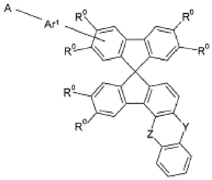

Fomule (I-3) Formule (I-4) 

Formule (I-5) Forumle (I-6) 

Formule (I-7) Formule (I-8) 

Formule (I-9) Formule (I-10) 

Formule (I-11) Formule (I-12) - Composé selon la revendication 1 ou 2, caractérisé en ce que A est un groupe de formule (A-1).
- Composé selon une ou plusieurs des revendications 1 à 3, caractérisé en ce que Ar1 est choisi, identique ou différent à chaque occurrence parmi une liaison simple ou un groupe divalent dérivé de benzène, biphényle, terphényle, fluorène, spirobifluorène, indénofluorène, carbazole, dibenzofurane, dibenzothiophène, en option substitué par des radicaux R2, ou une combinaison de deux ou plus de deux de ces groupes, mais pas plus de 30 atomes formant le cycle aromatique ne pouvant être présents dans Ar1
- Composé selon une ou plusieurs des revendications 1 à 4, caractérisé en ce que Ar2 est choisi, identique ou différent à chaque occurrence parmi les groupes phényle, biphényle, terphényle, fluorényle, spirobifluorényle, indénofluorényle, naphtyle, phénanthrényle, furanyle, benzofuranyle, dibenzofuranyle, thiophényle, benzothiophényle, dibenzothiophényle, carbazolyle, indolocarbazolyle et indénocarbazolyle, qui peuvent être substitués chacun par un ou plusieurs radicaux R2.
- Composé selon une ou plusieurs des revendications 1 à 5, caractérisé en ce que X est une liaison simple.
- Composé selon une ou plusieurs des revendications 1 à 6, caractérisé en ce que R1 et R2 sont, identiques ou différents à chaque occurrence, H, D, F, CN, un groupe alkyle à chaîne droite ayant de 1 à 10 atomes de carbone ou un groupe alkyle ramifié ou cyclique ayant de 3 à 10 atomes de carbone, ou un système cyclique aromatique ou hétéroaromatique ayant de 6 à 25 atomes formant le cycle aromatique, les groupes alkyle et alcoxy cités et les systèmes cycliques aromatiques ou hétéroaromatiques cités pouvant être substitués chacun par un ou plusieurs radicaux R3.
- Composé selon une ou plusieurs des revendications 1 à 7, caractérisé en ce que p est égal à 1, et en ce que tous les autres indices k, i, m et n sont égaux à 0, ou caractérisé en ce que k est égal à 1, et en ce que tous les autres indices i, m, n et p sont égaux à 0.
- Composé selon une ou plusieurs des revendications 1 à 8, caractérisé en ce que la somme des indices i, k, m, n et p est égale à 1.
- Composé selon une ou plusieurs des revendications 1 à 9, caractérisé en ce que le groupe Y représente S et le groupe Z représente O, S ou une liaison simple.
- Composé selon une ou plusieurs des revendications 1 à 10, caractérisé en ce que le groupe Y représente S, et le groupe Z est une liaison simple.
- Procédé pour la préparation d'un composé selon une ou plusieurs des revendications 1 à 11, caractérisé en ce que soitA) d'abord la structure de base spirobifluorène substituée par un groupe réactif est préparée par réaction d'un dérivé de dibenzothiophényle avec un dérivé de fluorénone, qui porte le groupe réactif, et dans une étape ultérieure un groupe diarylamino ou un groupe carbazole ou un groupe aryle ou hétéroaryle qui est substitué par un groupe diarylamino ou carbazole, est introduit, par une réaction de couplage organométallique, à la position du groupe réactif, soitB) est comprise la réaction d'un dérivé de dibenzothiophényle avec une fluorénone qui porte un groupe diarylamino ou un groupe carbazole ou un groupe aryle ou hétéroaryle qui est substitué par un groupe diarylamino ou carbazole, ouC) d'abord une structure de base spirobifluorène est préparée par réaction d'un dérivé de dibenzothiophényle avec un dérivé de fluorénone, puis elle est fonctionnalisée avec un groupe réactif, et dans une étape ultérieure un groupe diarylamino ou un groupe carbazole ou un groupe aryle ou hétéroaryle qui est substitué par un groupe diarylamino ou carbazole, est introduit, par une réaction de couplage organométallique, à la position du groupe réactif.
- Oligomère, polymère ou dendrimère, contenant un ou plusieurs composés de formule (I) selon une ou plusieurs des revendications 1 à 11, la/les liaison(s) au polymère, à l'oligomère ou au dendrimère pouvant être localisée(s) en des quelconques positions substituées par R0, R1 ou R2 dans la formule (I).
- Formulation, contenant au moins un composé selon une ou plusieurs des revendications 1 à 11, ou au moins un polymère, oligomère ou dendrimère selon la revendication 13, ainsi qu'au moins un solvant.
- Utilisation d'un composé selon une ou plusieurs des revendications 1 à 11 ou d'un oligomère, polymère ou dendrimère selon la revendication 13 dans un dispositif électronique.
- Dispositif électronique, contenant au moins un composé selon une ou plusieurs des revendications 1 à 11 ou au moins un oligomère, polymère ou dendrimère selon la revendication 13.
- Dispositif électronique selon la revendication 16, choisi dans le groupe constitué par les circuits intégrés organiques (OIC), les transistors à effet de champ organiques (OFET), les transistors en couches minces organiques (OTFT), les transistors électroluminescents organiques (OLET), les cellules solaires organiques (OSC), les détecteurs optiques organiques, les photorécepteurs organiques, les dispositifs à extinction de champ organiques (OFQD), les cellules électrochimiques électroluminescentes organiques (OLEC), les diodes laser organiques (O-Laser) et les dispositifs électroluminescents organiques (OLED).
- Dispositif électroluminescent organique selon la revendication 17, caractérisé en ce que ledit au moins un composé ou ledit au moins un oligomère, polymère ou dendrimère est présent dans une couche choisie parmi les couches de transport de trous et les couches émettrices.
- Dispositif électroluminescent organique selon la revendication 18, caractérisé en ce que ledit au moins un composé ou ledit au moins un oligomère, polymère ou dendrimère est présent dans une couche émettrice conjointement avec un ou plusieurs émetteurs phosphorescents.
- Dispositif électroluminescent organique selon la revendication 18, caractérisé en ce que ledit au moins un composé ou ledit au moins un oligomère, polymère ou dendrimère est présent dans une couche de transport de trous avec un ou plusieurs dopants p.
Applications Claiming Priority (2)
| Application Number | Priority Date | Filing Date | Title |
|---|---|---|---|
| EP14004355 | 2014-12-22 | ||
| PCT/EP2015/002475 WO2016102048A1 (fr) | 2014-12-22 | 2015-12-08 | Matériaux pour dispositifs électroniques |
Publications (2)
| Publication Number | Publication Date |
|---|---|
| EP3238286A1 EP3238286A1 (fr) | 2017-11-01 |
| EP3238286B1 true EP3238286B1 (fr) | 2024-01-17 |
Family
ID=52144366
Family Applications (1)
| Application Number | Title | Priority Date | Filing Date |
|---|---|---|---|
| EP15805398.3A Active EP3238286B1 (fr) | 2014-12-22 | 2015-12-08 | Matériaux pour dispositifs électroniques |
Country Status (7)
| Country | Link |
|---|---|
| US (1) | US10224492B2 (fr) |
| EP (1) | EP3238286B1 (fr) |
| JP (1) | JP6608451B2 (fr) |
| KR (1) | KR102069495B1 (fr) |
| CN (1) | CN107112439B (fr) |
| TW (1) | TWI684592B (fr) |
| WO (1) | WO2016102048A1 (fr) |
Families Citing this family (54)
| Publication number | Priority date | Publication date | Assignee | Title |
|---|---|---|---|---|
| KR102424977B1 (ko) * | 2015-04-14 | 2022-07-26 | 삼성디스플레이 주식회사 | 축합환 화합물 및 이를 포함한 유기 발광 소자 |
| KR102630644B1 (ko) | 2015-12-17 | 2024-01-30 | 삼성디스플레이 주식회사 | 유기 발광 소자 |
| CN113214202B (zh) * | 2016-02-25 | 2023-11-21 | 株式会社Lg化学 | 杂环化合物和包含其的有机发光二极管 |
| EP3464244B1 (fr) * | 2016-06-03 | 2021-11-17 | Merck Patent GmbH | Matériaux pour dispositifs électroluminescents organiques |
| US10693075B2 (en) * | 2016-08-09 | 2020-06-23 | Shanghai Nichem Fine Chemical Co., Ltd. | Spiro compound and organic electronic device comprising the same |
| TWI764942B (zh) | 2016-10-10 | 2022-05-21 | 德商麥克專利有限公司 | 電子裝置 |
| KR102683884B1 (ko) | 2016-11-02 | 2024-07-11 | 메르크 파텐트 게엠베하 | 전자 소자용 재료 |
| TW201833118A (zh) | 2016-11-22 | 2018-09-16 | 德商麥克專利有限公司 | 用於電子裝置之材料 |
| CN110325524A (zh) | 2017-03-02 | 2019-10-11 | 默克专利有限公司 | 用于有机电子器件的材料 |
| EP3615542B1 (fr) | 2017-04-25 | 2023-08-23 | Merck Patent GmbH | Composés pour dispositifs électroniques |
| US11767299B2 (en) | 2017-06-23 | 2023-09-26 | Merck Patent Gmbh | Materials for organic electroluminescent devices |
| WO2019002190A1 (fr) | 2017-06-28 | 2019-01-03 | Merck Patent Gmbh | Matériaux pour dispositifs électroniques |
| KR102393153B1 (ko) * | 2017-07-27 | 2022-05-02 | 에스에프씨주식회사 | 저전압 구동이 가능하며, 고효율 및 장수명 특성을 가지는 유기 발광 소자 |
| US20200212301A1 (en) | 2017-07-28 | 2020-07-02 | Merck Patent Gmbh | Spirobifluorene derivatives for use in electronic devices |
| CN109427985B (zh) * | 2017-08-31 | 2019-12-24 | 昆山国显光电有限公司 | 有机电致发光器件及显示装置 |
| EP3679024B1 (fr) | 2017-09-08 | 2022-11-02 | Merck Patent GmbH | Matériaux pour dispositifs électroniques |
| KR102109789B1 (ko) * | 2017-10-19 | 2020-05-12 | 주식회사 엘지화학 | 신규한 화합물 및 이를 이용한 유기발광 소자 |
| KR20250086794A (ko) | 2017-12-15 | 2025-06-13 | 메르크 파텐트 게엠베하 | 유기 전계 발광 디바이스용 치환된 방향족 아민 |
| EP3765444B1 (fr) | 2018-03-16 | 2026-01-14 | Merck Patent GmbH | Matériaux pour dispositifs électroluminescents organiques |
| JP7325731B2 (ja) | 2018-08-23 | 2023-08-15 | 国立大学法人九州大学 | 有機エレクトロルミネッセンス素子 |
| CN113227105A (zh) * | 2018-11-29 | 2021-08-06 | 默克专利有限公司 | 电子器件 |
| EP3898603A1 (fr) * | 2018-12-20 | 2021-10-27 | Merck Patent GmbH | Matériaux pour dispositifs électroniques |
| DE102019005700A1 (de) * | 2019-08-15 | 2021-02-18 | Merck Patent Gmbh | Elektronische Vorrichtung |
| CN114106003B (zh) * | 2020-08-31 | 2023-05-16 | 上海和辉光电股份有限公司 | 一种化合物及其应用 |
| JP7665314B2 (ja) | 2020-11-02 | 2025-04-21 | キヤノン株式会社 | 有機化合物及び有機発光素子 |
| KR20230104195A (ko) * | 2020-11-03 | 2023-07-07 | 메르크 파텐트 게엠베하 | 전자 디바이스용 재료 |
| KR20220086763A (ko) * | 2020-12-16 | 2022-06-24 | 주식회사 센텀머티리얼즈 | 신규한 스피로플루오렌 화합물 및 이를 포함하는 유기 발광 소자 |
| CN112375053B (zh) * | 2021-01-13 | 2021-04-16 | 南京高光半导体材料有限公司 | 一种化合物及有机电致发光器件 |
| CN112375054B (zh) * | 2021-01-13 | 2021-05-25 | 南京高光半导体材料有限公司 | 一种化合物及有机电致发光器件 |
| EP4410071A1 (fr) | 2021-09-28 | 2024-08-07 | Merck Patent GmbH | Matériaux pour dispositifs électroniques |
| CN118056486A (zh) | 2021-09-28 | 2024-05-17 | 默克专利有限公司 | 用于电子器件的材料 |
| WO2023052272A1 (fr) | 2021-09-28 | 2023-04-06 | Merck Patent Gmbh | Matériaux pour dispositifs électroniques |
| EP4410074B1 (fr) | 2021-09-28 | 2025-05-21 | Merck Patent GmbH | Matériaux pour dispositifs électroniques |
| CN113845505B (zh) * | 2021-10-20 | 2023-04-28 | 上海钥熠电子科技有限公司 | 螺芴衍生物类胺化合物和包含其的有机电致发光器件 |
| EP4437814A1 (fr) | 2021-11-25 | 2024-10-02 | Merck Patent GmbH | Matériaux pour dispositifs électroniques |
| KR20240128020A (ko) | 2021-12-21 | 2024-08-23 | 메르크 파텐트 게엠베하 | 중수소화 유기 화합물의 제조 방법 |
| EP4479385A1 (fr) | 2022-02-14 | 2024-12-25 | Merck Patent GmbH | Matériaux pour dispositifs électroniques |
| CN119156361A (zh) | 2022-05-18 | 2024-12-17 | 默克专利有限公司 | 用于氘化的有机化合物的制备方法 |
| CN119452060A (zh) | 2022-07-11 | 2025-02-14 | 默克专利有限公司 | 用于电子器件的材料 |
| EP4640022A1 (fr) | 2022-12-19 | 2025-10-29 | Merck Patent GmbH | Matériaux pour dispositifs électroniques |
| CN120379953A (zh) | 2022-12-20 | 2025-07-25 | 默克专利有限公司 | 用于制备氘化芳族化合物的方法 |
| KR20250151490A (ko) | 2023-02-17 | 2025-10-21 | 메르크 파텐트 게엠베하 | 유기 전계발광 디바이스용 재료 |
| KR20260015809A (ko) | 2023-04-20 | 2026-02-03 | 메르크 파텐트 게엠베하 | 전자 디바이스들을 위한 재료들 |
| EP4720070A1 (fr) | 2023-05-25 | 2026-04-08 | Merck Patent GmbH | Dérivés de tris[1,2,4]triazolo[1,5-a:1',5'-c:1'',5''-e][1,3,5]triazine destinés à être utilisés dans des dispositifs électroluminescents organiques |
| CN121487940A (zh) | 2023-07-12 | 2026-02-06 | 默克专利有限公司 | 用于电子器件的材料 |
| KR20260044229A (ko) | 2023-07-27 | 2026-04-01 | 메르크 파텐트 게엠베하 | 유기 발광 디바이스 및 유기 센서를 위한 재료 |
| WO2025045842A1 (fr) | 2023-08-30 | 2025-03-06 | Merck Patent Gmbh | Matériaux pour dispositifs électroluminescents organiques |
| CN121753521A (zh) | 2023-08-30 | 2026-03-27 | 默克专利有限公司 | 用于有机发光器件的材料 |
| CN121773745A (zh) | 2023-08-30 | 2026-03-31 | 默克专利有限公司 | 用于有机发光器件的材料 |
| WO2025083015A1 (fr) | 2023-10-19 | 2025-04-24 | Merck Patent Gmbh | Matériaux pour dispositifs électroluminescents organiques |
| WO2025132547A1 (fr) | 2023-12-21 | 2025-06-26 | Merck Patent Gmbh | Procédé mécanochimique de deutération de composés organiques |
| WO2025132551A1 (fr) | 2023-12-22 | 2025-06-26 | Merck Patent Gmbh | Matériaux pour dispositifs électroniques |
| WO2025196145A1 (fr) | 2024-03-22 | 2025-09-25 | Merck Patent Gmbh | Matériaux pour dispositifs électroluminescents organiques |
| WO2025210013A1 (fr) | 2024-04-04 | 2025-10-09 | Merck Patent Gmbh | Composés pour dispositifs électroniques, en particulier composés pour oled |
Family Cites Families (7)
| Publication number | Priority date | Publication date | Assignee | Title |
|---|---|---|---|---|
| KR101423173B1 (ko) * | 2010-11-04 | 2014-07-25 | 제일모직 주식회사 | 유기광전소자용 화합물 및 이를 포함하는 유기광전소자 |
| KR101507001B1 (ko) * | 2011-12-30 | 2015-03-31 | 제일모직 주식회사 | 유기광전자소자용 화합물, 이를 포함하는 유기발광소자 및 상기 유기발광소자를 포함하는 표시장치 |
| KR102015765B1 (ko) * | 2012-02-14 | 2019-10-21 | 메르크 파텐트 게엠베하 | 유기 전계발광 소자용 스피로비플루오렌 화합물 |
| KR101537005B1 (ko) * | 2012-09-28 | 2015-07-20 | 제일모직 주식회사 | 유기광전자소자용 화합물, 이를 포함하는 유기발광소자 및 상기 유기발광소자를 포함하는 표시장치 |
| WO2014129846A1 (fr) * | 2013-02-21 | 2014-08-28 | Rohm And Haas Electronic Materials Korea Ltd. | Composés électroluminescents organiques et dispositif électroluminescent organique comprenant ces composés |
| JP6567520B2 (ja) * | 2013-08-15 | 2019-08-28 | メルク パテント ゲーエムベーハー | 電子素子のための材料 |
| WO2016131521A1 (fr) * | 2015-02-16 | 2016-08-25 | Merck Patent Gmbh | Matériaux à base de dérivés de spirobifluorène pour dispositifs électroniques |
-
2015
- 2015-12-08 US US15/538,277 patent/US10224492B2/en active Active
- 2015-12-08 WO PCT/EP2015/002475 patent/WO2016102048A1/fr not_active Ceased
- 2015-12-08 KR KR1020177020112A patent/KR102069495B1/ko active Active
- 2015-12-08 JP JP2017533842A patent/JP6608451B2/ja active Active
- 2015-12-08 EP EP15805398.3A patent/EP3238286B1/fr active Active
- 2015-12-08 CN CN201580070275.5A patent/CN107112439B/zh active Active
- 2015-12-17 TW TW104142514A patent/TWI684592B/zh not_active IP Right Cessation
Also Published As
| Publication number | Publication date |
|---|---|
| CN107112439B (zh) | 2020-04-10 |
| US10224492B2 (en) | 2019-03-05 |
| EP3238286A1 (fr) | 2017-11-01 |
| CN107112439A (zh) | 2017-08-29 |
| TWI684592B (zh) | 2020-02-11 |
| US20180006245A1 (en) | 2018-01-04 |
| KR102069495B1 (ko) | 2020-01-23 |
| TW201638079A (zh) | 2016-11-01 |
| WO2016102048A1 (fr) | 2016-06-30 |
| JP6608451B2 (ja) | 2019-11-20 |
| KR20170097163A (ko) | 2017-08-25 |
| JP2018503619A (ja) | 2018-02-08 |
Similar Documents
| Publication | Publication Date | Title |
|---|---|---|
| EP3238286B1 (fr) | Matériaux pour dispositifs électroniques | |
| EP3259330B1 (fr) | Matériaux à base de dérivés de spirobifluorène pour dispositifs électroniques | |
| EP3033405B1 (fr) | Matériaux destinés à des dispositifs électroniques | |
| EP3378857B1 (fr) | Matériaux pour dispositifs électroniques | |
| EP3114102B1 (fr) | Materiaux pour dispositifs electroniques | |
| EP3131901B1 (fr) | Matières pour dispositifs électroniques | |
| EP3132476B1 (fr) | Matières pour dispositifs électroniques | |
| EP3693437B1 (fr) | Composés et dispositifs électro-organiques | |
| EP2875092B1 (fr) | Composés et dispositifs electroluminescents organiques | |
| EP2737554B1 (fr) | Composés pour dispositifs électroniques | |
| WO2018083053A1 (fr) | Matériaux pour dispositifs électroniques | |
| EP3017016A1 (fr) | Matériaux pour dispositifs électroniques | |
| EP3057947A2 (fr) | Matériaux pour dispositifs électroniques | |
| EP2926385B1 (fr) | Dispositif électronique | |
| EP3615542B1 (fr) | Composés pour dispositifs électroniques | |
| EP3775099A1 (fr) | Matériaux pour dispositifs électroniques | |
| WO2014106524A2 (fr) | Matériaux pour dispositifs électroniques | |
| EP3544986A1 (fr) | Triarylamines pontées destinées à des dispositifs électroniques | |
| WO2022096172A1 (fr) | Matériaux pour dispositifs électroniques | |
| EP3679023A1 (fr) | Matériaux pour dispositifs électroniques | |
| WO2021214348A2 (fr) | Composés pour dispositifs électroniques | |
| WO2017108152A1 (fr) | Matériaux pour dispositifs électroniques |
Legal Events
| Date | Code | Title | Description |
|---|---|---|---|
| STAA | Information on the status of an ep patent application or granted ep patent |
Free format text: STATUS: THE INTERNATIONAL PUBLICATION HAS BEEN MADE |
|
| PUAI | Public reference made under article 153(3) epc to a published international application that has entered the european phase |
Free format text: ORIGINAL CODE: 0009012 |
|
| STAA | Information on the status of an ep patent application or granted ep patent |
Free format text: STATUS: REQUEST FOR EXAMINATION WAS MADE |
|
| 17P | Request for examination filed |
Effective date: 20170609 |
|
| AK | Designated contracting states |
Kind code of ref document: A1 Designated state(s): AL AT BE BG CH CY CZ DE DK EE ES FI FR GB GR HR HU IE IS IT LI LT LU LV MC MK MT NL NO PL PT RO RS SE SI SK SM TR |
|
| AX | Request for extension of the european patent |
Extension state: BA ME |
|
| DAV | Request for validation of the european patent (deleted) | ||
| DAX | Request for extension of the european patent (deleted) | ||
| STAA | Information on the status of an ep patent application or granted ep patent |
Free format text: STATUS: EXAMINATION IS IN PROGRESS |
|
| 17Q | First examination report despatched |
Effective date: 20200120 |
|
| RAP3 | Party data changed (applicant data changed or rights of an application transferred) |
Owner name: MERCK PATENT GMBH |
|
| P01 | Opt-out of the competence of the unified patent court (upc) registered |
Effective date: 20230518 |
|
| REG | Reference to a national code |
Ref country code: DE Ref legal event code: R079 Free format text: PREVIOUS MAIN CLASS: H01L0051540000 Ipc: H10K0085600000 Ref country code: DE Ref legal event code: R079 Ref document number: 502015016739 Country of ref document: DE Free format text: PREVIOUS MAIN CLASS: H01L0051540000 Ipc: H10K0085600000 |
|
| GRAP | Despatch of communication of intention to grant a patent |
Free format text: ORIGINAL CODE: EPIDOSNIGR1 |
|
| STAA | Information on the status of an ep patent application or granted ep patent |
Free format text: STATUS: GRANT OF PATENT IS INTENDED |
|
| RIC1 | Information provided on ipc code assigned before grant |
Ipc: H10K 30/00 20230101ALN20230823BHEP Ipc: H10K 10/46 20230101ALN20230823BHEP Ipc: H10K 50/155 20230101ALN20230823BHEP Ipc: H10K 85/60 20230101AFI20230823BHEP |
|
| INTG | Intention to grant announced |
Effective date: 20230911 |
|
| GRAS | Grant fee paid |
Free format text: ORIGINAL CODE: EPIDOSNIGR3 |
|
| GRAA | (expected) grant |
Free format text: ORIGINAL CODE: 0009210 |
|
| STAA | Information on the status of an ep patent application or granted ep patent |
Free format text: STATUS: THE PATENT HAS BEEN GRANTED |
|
| AK | Designated contracting states |
Kind code of ref document: B1 Designated state(s): AL AT BE BG CH CY CZ DE DK EE ES FI FR GB GR HR HU IE IS IT LI LT LU LV MC MK MT NL NO PL PT RO RS SE SI SK SM TR |
|
| REG | Reference to a national code |
Ref country code: GB Ref legal event code: FG4D Free format text: NOT ENGLISH |
|
| REG | Reference to a national code |
Ref country code: DE Ref legal event code: R096 Ref document number: 502015016739 Country of ref document: DE |
|
| REG | Reference to a national code |
Ref country code: CH Ref legal event code: EP |
|
| REG | Reference to a national code |
Ref country code: IE Ref legal event code: FG4D Free format text: LANGUAGE OF EP DOCUMENT: GERMAN |
|
| REG | Reference to a national code |
Ref country code: LT Ref legal event code: MG9D |
|
| REG | Reference to a national code |
Ref country code: NL Ref legal event code: MP Effective date: 20240117 |
|
| PG25 | Lapsed in a contracting state [announced via postgrant information from national office to epo] |
Ref country code: NL Free format text: LAPSE BECAUSE OF FAILURE TO SUBMIT A TRANSLATION OF THE DESCRIPTION OR TO PAY THE FEE WITHIN THE PRESCRIBED TIME-LIMIT Effective date: 20240117 |
|
| PG25 | Lapsed in a contracting state [announced via postgrant information from national office to epo] |
Ref country code: NL Free format text: LAPSE BECAUSE OF FAILURE TO SUBMIT A TRANSLATION OF THE DESCRIPTION OR TO PAY THE FEE WITHIN THE PRESCRIBED TIME-LIMIT Effective date: 20240117 |
|
| PG25 | Lapsed in a contracting state [announced via postgrant information from national office to epo] |
Ref country code: IS Free format text: LAPSE BECAUSE OF FAILURE TO SUBMIT A TRANSLATION OF THE DESCRIPTION OR TO PAY THE FEE WITHIN THE PRESCRIBED TIME-LIMIT Effective date: 20240517 |
|
| PG25 | Lapsed in a contracting state [announced via postgrant information from national office to epo] |
Ref country code: LT Free format text: LAPSE BECAUSE OF FAILURE TO SUBMIT A TRANSLATION OF THE DESCRIPTION OR TO PAY THE FEE WITHIN THE PRESCRIBED TIME-LIMIT Effective date: 20240117 |
|
| PG25 | Lapsed in a contracting state [announced via postgrant information from national office to epo] |
Ref country code: GR Free format text: LAPSE BECAUSE OF FAILURE TO SUBMIT A TRANSLATION OF THE DESCRIPTION OR TO PAY THE FEE WITHIN THE PRESCRIBED TIME-LIMIT Effective date: 20240418 |
|
| PG25 | Lapsed in a contracting state [announced via postgrant information from national office to epo] |
Ref country code: HR Free format text: LAPSE BECAUSE OF FAILURE TO SUBMIT A TRANSLATION OF THE DESCRIPTION OR TO PAY THE FEE WITHIN THE PRESCRIBED TIME-LIMIT Effective date: 20240117 Ref country code: RS Free format text: LAPSE BECAUSE OF FAILURE TO SUBMIT A TRANSLATION OF THE DESCRIPTION OR TO PAY THE FEE WITHIN THE PRESCRIBED TIME-LIMIT Effective date: 20240417 |
|
| PG25 | Lapsed in a contracting state [announced via postgrant information from national office to epo] |
Ref country code: ES Free format text: LAPSE BECAUSE OF FAILURE TO SUBMIT A TRANSLATION OF THE DESCRIPTION OR TO PAY THE FEE WITHIN THE PRESCRIBED TIME-LIMIT Effective date: 20240117 |
|
| PG25 | Lapsed in a contracting state [announced via postgrant information from national office to epo] |
Ref country code: RS Free format text: LAPSE BECAUSE OF FAILURE TO SUBMIT A TRANSLATION OF THE DESCRIPTION OR TO PAY THE FEE WITHIN THE PRESCRIBED TIME-LIMIT Effective date: 20240417 Ref country code: NO Free format text: LAPSE BECAUSE OF FAILURE TO SUBMIT A TRANSLATION OF THE DESCRIPTION OR TO PAY THE FEE WITHIN THE PRESCRIBED TIME-LIMIT Effective date: 20240417 Ref country code: LT Free format text: LAPSE BECAUSE OF FAILURE TO SUBMIT A TRANSLATION OF THE DESCRIPTION OR TO PAY THE FEE WITHIN THE PRESCRIBED TIME-LIMIT Effective date: 20240117 Ref country code: IS Free format text: LAPSE BECAUSE OF FAILURE TO SUBMIT A TRANSLATION OF THE DESCRIPTION OR TO PAY THE FEE WITHIN THE PRESCRIBED TIME-LIMIT Effective date: 20240517 Ref country code: HR Free format text: LAPSE BECAUSE OF FAILURE TO SUBMIT A TRANSLATION OF THE DESCRIPTION OR TO PAY THE FEE WITHIN THE PRESCRIBED TIME-LIMIT Effective date: 20240117 Ref country code: GR Free format text: LAPSE BECAUSE OF FAILURE TO SUBMIT A TRANSLATION OF THE DESCRIPTION OR TO PAY THE FEE WITHIN THE PRESCRIBED TIME-LIMIT Effective date: 20240418 Ref country code: FI Free format text: LAPSE BECAUSE OF FAILURE TO SUBMIT A TRANSLATION OF THE DESCRIPTION OR TO PAY THE FEE WITHIN THE PRESCRIBED TIME-LIMIT Effective date: 20240117 Ref country code: ES Free format text: LAPSE BECAUSE OF FAILURE TO SUBMIT A TRANSLATION OF THE DESCRIPTION OR TO PAY THE FEE WITHIN THE PRESCRIBED TIME-LIMIT Effective date: 20240117 Ref country code: BG Free format text: LAPSE BECAUSE OF FAILURE TO SUBMIT A TRANSLATION OF THE DESCRIPTION OR TO PAY THE FEE WITHIN THE PRESCRIBED TIME-LIMIT Effective date: 20240117 |
|
| PG25 | Lapsed in a contracting state [announced via postgrant information from national office to epo] |
Ref country code: PT Free format text: LAPSE BECAUSE OF FAILURE TO SUBMIT A TRANSLATION OF THE DESCRIPTION OR TO PAY THE FEE WITHIN THE PRESCRIBED TIME-LIMIT Effective date: 20240517 Ref country code: PL Free format text: LAPSE BECAUSE OF FAILURE TO SUBMIT A TRANSLATION OF THE DESCRIPTION OR TO PAY THE FEE WITHIN THE PRESCRIBED TIME-LIMIT Effective date: 20240117 |
|
| PG25 | Lapsed in a contracting state [announced via postgrant information from national office to epo] |
Ref country code: SE Free format text: LAPSE BECAUSE OF FAILURE TO SUBMIT A TRANSLATION OF THE DESCRIPTION OR TO PAY THE FEE WITHIN THE PRESCRIBED TIME-LIMIT Effective date: 20240117 Ref country code: PT Free format text: LAPSE BECAUSE OF FAILURE TO SUBMIT A TRANSLATION OF THE DESCRIPTION OR TO PAY THE FEE WITHIN THE PRESCRIBED TIME-LIMIT Effective date: 20240517 Ref country code: PL Free format text: LAPSE BECAUSE OF FAILURE TO SUBMIT A TRANSLATION OF THE DESCRIPTION OR TO PAY THE FEE WITHIN THE PRESCRIBED TIME-LIMIT Effective date: 20240117 Ref country code: LV Free format text: LAPSE BECAUSE OF FAILURE TO SUBMIT A TRANSLATION OF THE DESCRIPTION OR TO PAY THE FEE WITHIN THE PRESCRIBED TIME-LIMIT Effective date: 20240117 |
|
| PG25 | Lapsed in a contracting state [announced via postgrant information from national office to epo] |
Ref country code: DK Free format text: LAPSE BECAUSE OF FAILURE TO SUBMIT A TRANSLATION OF THE DESCRIPTION OR TO PAY THE FEE WITHIN THE PRESCRIBED TIME-LIMIT Effective date: 20240117 |
|
| PG25 | Lapsed in a contracting state [announced via postgrant information from national office to epo] |
Ref country code: SM Free format text: LAPSE BECAUSE OF FAILURE TO SUBMIT A TRANSLATION OF THE DESCRIPTION OR TO PAY THE FEE WITHIN THE PRESCRIBED TIME-LIMIT Effective date: 20240117 |
|
| REG | Reference to a national code |
Ref country code: DE Ref legal event code: R097 Ref document number: 502015016739 Country of ref document: DE |
|
| PG25 | Lapsed in a contracting state [announced via postgrant information from national office to epo] |
Ref country code: CZ Free format text: LAPSE BECAUSE OF FAILURE TO SUBMIT A TRANSLATION OF THE DESCRIPTION OR TO PAY THE FEE WITHIN THE PRESCRIBED TIME-LIMIT Effective date: 20240117 Ref country code: EE Free format text: LAPSE BECAUSE OF FAILURE TO SUBMIT A TRANSLATION OF THE DESCRIPTION OR TO PAY THE FEE WITHIN THE PRESCRIBED TIME-LIMIT Effective date: 20240117 |
|
| PG25 | Lapsed in a contracting state [announced via postgrant information from national office to epo] |
Ref country code: SK Free format text: LAPSE BECAUSE OF FAILURE TO SUBMIT A TRANSLATION OF THE DESCRIPTION OR TO PAY THE FEE WITHIN THE PRESCRIBED TIME-LIMIT Effective date: 20240117 |
|
| PG25 | Lapsed in a contracting state [announced via postgrant information from national office to epo] |
Ref country code: SM Free format text: LAPSE BECAUSE OF FAILURE TO SUBMIT A TRANSLATION OF THE DESCRIPTION OR TO PAY THE FEE WITHIN THE PRESCRIBED TIME-LIMIT Effective date: 20240117 Ref country code: SK Free format text: LAPSE BECAUSE OF FAILURE TO SUBMIT A TRANSLATION OF THE DESCRIPTION OR TO PAY THE FEE WITHIN THE PRESCRIBED TIME-LIMIT Effective date: 20240117 Ref country code: RO Free format text: LAPSE BECAUSE OF FAILURE TO SUBMIT A TRANSLATION OF THE DESCRIPTION OR TO PAY THE FEE WITHIN THE PRESCRIBED TIME-LIMIT Effective date: 20240117 Ref country code: EE Free format text: LAPSE BECAUSE OF FAILURE TO SUBMIT A TRANSLATION OF THE DESCRIPTION OR TO PAY THE FEE WITHIN THE PRESCRIBED TIME-LIMIT Effective date: 20240117 Ref country code: DK Free format text: LAPSE BECAUSE OF FAILURE TO SUBMIT A TRANSLATION OF THE DESCRIPTION OR TO PAY THE FEE WITHIN THE PRESCRIBED TIME-LIMIT Effective date: 20240117 Ref country code: CZ Free format text: LAPSE BECAUSE OF FAILURE TO SUBMIT A TRANSLATION OF THE DESCRIPTION OR TO PAY THE FEE WITHIN THE PRESCRIBED TIME-LIMIT Effective date: 20240117 |
|
| PLBE | No opposition filed within time limit |
Free format text: ORIGINAL CODE: 0009261 |
|
| STAA | Information on the status of an ep patent application or granted ep patent |
Free format text: STATUS: NO OPPOSITION FILED WITHIN TIME LIMIT |
|
| PG25 | Lapsed in a contracting state [announced via postgrant information from national office to epo] |
Ref country code: IT Free format text: LAPSE BECAUSE OF FAILURE TO SUBMIT A TRANSLATION OF THE DESCRIPTION OR TO PAY THE FEE WITHIN THE PRESCRIBED TIME-LIMIT Effective date: 20240117 |
|
| 26N | No opposition filed |
Effective date: 20241018 |
|
| PG25 | Lapsed in a contracting state [announced via postgrant information from national office to epo] |
Ref country code: IT Free format text: LAPSE BECAUSE OF FAILURE TO SUBMIT A TRANSLATION OF THE DESCRIPTION OR TO PAY THE FEE WITHIN THE PRESCRIBED TIME-LIMIT Effective date: 20240117 |
|
| PG25 | Lapsed in a contracting state [announced via postgrant information from national office to epo] |
Ref country code: SI Free format text: LAPSE BECAUSE OF FAILURE TO SUBMIT A TRANSLATION OF THE DESCRIPTION OR TO PAY THE FEE WITHIN THE PRESCRIBED TIME-LIMIT Effective date: 20240117 |
|
| PG25 | Lapsed in a contracting state [announced via postgrant information from national office to epo] |
Ref country code: MC Free format text: LAPSE BECAUSE OF FAILURE TO SUBMIT A TRANSLATION OF THE DESCRIPTION OR TO PAY THE FEE WITHIN THE PRESCRIBED TIME-LIMIT Effective date: 20240117 |
|
| REG | Reference to a national code |
Ref country code: CH Ref legal event code: PL |
|
| PG25 | Lapsed in a contracting state [announced via postgrant information from national office to epo] |
Ref country code: LU Free format text: LAPSE BECAUSE OF NON-PAYMENT OF DUE FEES Effective date: 20241208 |
|
| GBPC | Gb: european patent ceased through non-payment of renewal fee |
Effective date: 20241208 |
|
| REG | Reference to a national code |
Ref country code: BE Ref legal event code: MM Effective date: 20241231 |
|
| PG25 | Lapsed in a contracting state [announced via postgrant information from national office to epo] |
Ref country code: GB Free format text: LAPSE BECAUSE OF NON-PAYMENT OF DUE FEES Effective date: 20241208 Ref country code: BE Free format text: LAPSE BECAUSE OF NON-PAYMENT OF DUE FEES Effective date: 20241231 |
|
| PG25 | Lapsed in a contracting state [announced via postgrant information from national office to epo] |
Ref country code: FR Free format text: LAPSE BECAUSE OF NON-PAYMENT OF DUE FEES Effective date: 20241231 |
|
| PG25 | Lapsed in a contracting state [announced via postgrant information from national office to epo] |
Ref country code: CH Free format text: LAPSE BECAUSE OF NON-PAYMENT OF DUE FEES Effective date: 20241231 |
|
| PG25 | Lapsed in a contracting state [announced via postgrant information from national office to epo] |
Ref country code: IE Free format text: LAPSE BECAUSE OF NON-PAYMENT OF DUE FEES Effective date: 20241208 |
|
| PGFP | Annual fee paid to national office [announced via postgrant information from national office to epo] |
Ref country code: DE Payment date: 20251126 Year of fee payment: 11 |
|
| REG | Reference to a national code |
Ref country code: AT Ref legal event code: MM01 Ref document number: 1651393 Country of ref document: AT Kind code of ref document: T Effective date: 20241208 |
|
| PG25 | Lapsed in a contracting state [announced via postgrant information from national office to epo] |
Ref country code: AT Free format text: LAPSE BECAUSE OF NON-PAYMENT OF DUE FEES Effective date: 20241208 |