EP3240039A1 - Transistor bipolaire à grille isolée latérale - Google Patents
Transistor bipolaire à grille isolée latérale Download PDFInfo
- Publication number
- EP3240039A1 EP3240039A1 EP15871728.0A EP15871728A EP3240039A1 EP 3240039 A1 EP3240039 A1 EP 3240039A1 EP 15871728 A EP15871728 A EP 15871728A EP 3240039 A1 EP3240039 A1 EP 3240039A1
- Authority
- EP
- European Patent Office
- Prior art keywords
- region
- bipolar transistor
- gate bipolar
- lateral insulated
- insulated gate
- Prior art date
- Legal status (The legal status is an assumption and is not a legal conclusion. Google has not performed a legal analysis and makes no representation as to the accuracy of the status listed.)
- Granted
Links
Images
Classifications
-
- H—ELECTRICITY
- H10—SEMICONDUCTOR DEVICES; ELECTRIC SOLID-STATE DEVICES NOT OTHERWISE PROVIDED FOR
- H10D—INORGANIC ELECTRIC SEMICONDUCTOR DEVICES
- H10D12/00—Bipolar devices controlled by the field effect, e.g. insulated-gate bipolar transistors [IGBT]
- H10D12/411—Insulated-gate bipolar transistors [IGBT]
- H10D12/421—Insulated-gate bipolar transistors [IGBT] on insulating layers or insulating substrates, e.g. thin-film IGBTs
-
- H—ELECTRICITY
- H10—SEMICONDUCTOR DEVICES; ELECTRIC SOLID-STATE DEVICES NOT OTHERWISE PROVIDED FOR
- H10D—INORGANIC ELECTRIC SEMICONDUCTOR DEVICES
- H10D12/00—Bipolar devices controlled by the field effect, e.g. insulated-gate bipolar transistors [IGBT]
- H10D12/411—Insulated-gate bipolar transistors [IGBT]
-
- H—ELECTRICITY
- H10—SEMICONDUCTOR DEVICES; ELECTRIC SOLID-STATE DEVICES NOT OTHERWISE PROVIDED FOR
- H10D—INORGANIC ELECTRIC SEMICONDUCTOR DEVICES
- H10D62/00—Semiconductor bodies, or regions thereof, of devices having potential barriers
- H10D62/10—Shapes, relative sizes or dispositions of the regions of the semiconductor bodies; Shapes of the semiconductor bodies
- H10D62/13—Semiconductor regions connected to electrodes carrying current to be rectified, amplified or switched, e.g. source or drain regions
- H10D62/141—Anode or cathode regions of thyristors; Collector or emitter regions of gated bipolar-mode devices, e.g. of IGBTs
- H10D62/142—Anode regions of thyristors or collector regions of gated bipolar-mode devices
Definitions
- the present invention relates to a semiconductor process, and particularly relates to a lateral insulated gate bipolar transistor.
- LIGBT Lateral Insulated-Gate Bipolar Transistor
- LDMOS Lateral Insulated-Gate Bipolar Transistor
- a lateral insulated gate bipolar transistor includes: a substrate; an anode terminal located on the substrate including: an N-type buffer region on the substrate; a P well in the N-type buffer region; an N-region located in the P well; two P+ shallow junctions located on a surface of the P well; and an N+ shallow junction located between the two P+ shallow junctions; a cathode terminal located on the substrate; a draft region between the anode terminal and cathode terminal; and a gate between the anode terminal and cathode terminal.
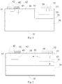
- Fig. 1 shows a cross sectional diagram of a lateral insulated gate bipolar transistor in an embodiment.
- the lateral insulated gate bipolar transistor includes a substrate 10, an anode terminal and a cathode terminal on the substrate 10, a drift region 30 and a gate 62 located between the anode terminal and the cathode terminal.
- the anode terminal includes an N-type buffer region 51 on the substrate; a P well 53 in the N-type buffer region 51; an N-region 55 located in the P well 53; two P+ shallow junctions 57 located on a surface of the P well 53; and an N+ shallow junction 59 located between the two P+ shallow junctions 57.
- the cathode terminal includes a P+ region 41 located on the substrate 10; a P-type body region 43 located between the P+ region 41 and the anode terminal; an N+ region 45 located at a surface of the P-type body region 43; and a cathode metal 42 as an electrode of the emitter.
- the gate 62 includes a gate oxide layer (not shown) and a polysilicon gate on the gate oxide layer.
- the gate 62 when the gate 62 is biased forwardly, the device channel is opened, the electronic current passes through the channel of the P-type body region 43 via the N+ region 45 of the emitter, and flows into the drift region 30 and the N-type buffer region 51 in sequence.
- the P+ shallow junctions 57 of the anode terminal when the P+ shallow junctions 57 of the anode terminal is biased forwardly and the bias voltage is lower, holes begin to inject into the N-type buffer region 51 downward from the P+ shallow junctions 57 and the P well 53 of the anode terminal; as the bias voltage on the anode metal 52 raises, the P+ shallow junctions 57 also inject holes into the drift region 30 laterally via the N-type buffer region 51, which achieves efficient majority carrier holes injection of multiple paths and significantly reduces the on-resistance.
- the anode When the lateral insulated gate bipolar transistor is turned off, the anode is biased inversely, a lower resistance path of electronic injection is formed by the N+ shallow junction 59, the N-region 55 and the N-type buffer region 51, and then residual minority carrier holes in the drift region 30 are extracted quickly to achieve a quick tuning-off, which ensures a quicker switching speed.
- the doped concentration of each region satisfies the following relationships: a doped concentration of the N-type buffer region 51 is less than a doped concentration of the P well 53; the doped concentration of the P well 53 is slightly less than a doped concentration of the N-region 55; and the doped concentration of the N-region 55 is less than doped concentrations of the two P+ shallow junctions 57 and the N+ shallow junction 59.
- the N-region 55 is a key of controlling lifetime of minority carrier and is designed to have a suitable doped concentration, which can form a longitudinal (the P+ shallow junctions 57 ⁇ the N-region 55 ⁇ the P well 53) VPNP.
- FIG. 2 illustrates the flow direction of holes when the anode is biased forwardly by an arrow.
- the one of two P+ shallow junctions 57 that is positioned closer to the cathode terminal and the N+ shallow junction 59 are disposed at a surface of the N-region 55.
- the doped concentration of the N-type buffer region 51 is 10 15 /cm3; the doped concentration of the P well 53 is 10 17 /cm 3 ; and the doped concentrations of the P+ shallow junctions 57 and the N+ shallow junction 59 are 10 20 /cm 3 .
- the anode terminal forms a deep and light N-type buffer region 51 firstly by injecting N-type ions and experiencing a drive-in process under a high temperature and for a long time, and minority carriers can be captured when the lateral insulated gate bipolar transistor is turned off.
- P-type ions are injected into the N-type buffer region 51 and the P well 53 is formed by thermal annealing; a N-region 55 of a longitudinal junction depth with a certain depth by injecting N-type ions and annealing; the N-region 55 serves as a channel of a certain width for injecting electrons and extracting holes, and then the P+ shallow junctions 57 and the N+ shallow junction 59 are formed by performing the injection process.
- SOI LIGBT devices widely apply in the automotive electronics, home electronics and communications and industrial applications due to a lower current leakage, a lower on-state resistance, a high input impedance, a high package density, a fast switching, a significant noise reduction effect and a working feasibility under high temperature caused by the trench isolation.
- the LIGBT shown in Fig. 1 is an silicon on insulator type lateral insulated gate bipolar transistor (SOI-LIGBT) includes a buried oxide layer 20 located between the substrate 10 and the draft region 30, wherein the substrate 10 is a P-type substrate, and the drift region 30 is an N-type drift region.
- the junction depth of the P+ region 41 is deeper and extends to the buried oxide layer 20.
Landscapes
- Insulated Gate Type Field-Effect Transistor (AREA)
- Thin Film Transistor (AREA)
- Bipolar Transistors (AREA)
- Thyristors (AREA)
Applications Claiming Priority (2)
| Application Number | Priority Date | Filing Date | Title |
|---|---|---|---|
| CN201410810523.2A CN105789286B (zh) | 2014-12-22 | 2014-12-22 | 横向绝缘栅双极型晶体管 |
| PCT/CN2015/089302 WO2016101654A1 (fr) | 2014-12-22 | 2015-09-10 | Transistor bipolaire à grille isolée latérale |
Publications (3)
| Publication Number | Publication Date |
|---|---|
| EP3240039A1 true EP3240039A1 (fr) | 2017-11-01 |
| EP3240039A4 EP3240039A4 (fr) | 2018-08-01 |
| EP3240039B1 EP3240039B1 (fr) | 2021-07-28 |
Family
ID=56149178
Family Applications (1)
| Application Number | Title | Priority Date | Filing Date |
|---|---|---|---|
| EP15871728.0A Active EP3240039B1 (fr) | 2014-12-22 | 2015-09-10 | Transistor bipolaire à grille isolée latérale |
Country Status (5)
| Country | Link |
|---|---|
| US (1) | US9905680B2 (fr) |
| EP (1) | EP3240039B1 (fr) |
| JP (1) | JP6430650B2 (fr) |
| CN (1) | CN105789286B (fr) |
| WO (1) | WO2016101654A1 (fr) |
Families Citing this family (2)
| Publication number | Priority date | Publication date | Assignee | Title |
|---|---|---|---|---|
| CN110010678A (zh) * | 2018-01-04 | 2019-07-12 | 中兴通讯股份有限公司 | 横向绝缘栅双极晶体管及其制作方法 |
| CN114937666B (zh) * | 2022-05-12 | 2025-03-25 | 重庆邮电大学 | 一种集成双自偏置mos低关断损耗的rc-ligbt器件 |
Family Cites Families (15)
| Publication number | Priority date | Publication date | Assignee | Title |
|---|---|---|---|---|
| US5396087A (en) * | 1992-12-14 | 1995-03-07 | North Carolina State University | Insulated gate bipolar transistor with reduced susceptibility to parasitic latch-up |
| JP3085037B2 (ja) * | 1993-08-18 | 2000-09-04 | 富士電機株式会社 | 絶縁ゲートバイポーラトランジスタ |
| GB2289371B (en) * | 1994-05-05 | 1997-11-19 | Fuji Electric Co Ltd | A semiconductor device and control method |
| US5665988A (en) * | 1995-02-09 | 1997-09-09 | Fuji Electric Co., Ltd. | Conductivity-modulation semiconductor |
| US5925900A (en) * | 1995-05-11 | 1999-07-20 | Fuji Electric Co., Ltd. | Emitter-switched thyristor having a floating ohmic contact |
| US5731603A (en) * | 1995-08-24 | 1998-03-24 | Kabushiki Kaisha Toshiba | Lateral IGBT |
| JP3367839B2 (ja) * | 1995-09-18 | 2003-01-20 | 株式会社東芝 | 半導体装置 |
| US7465964B2 (en) * | 2005-12-30 | 2008-12-16 | Cambridge Semiconductor Limited | Semiconductor device in which an injector region is isolated from a substrate |
| CN2914330Y (zh) | 2006-05-24 | 2007-06-20 | 杭州电子科技大学 | 抗esd的集成soi ligbt器件单元 |
| US7605446B2 (en) * | 2006-07-14 | 2009-10-20 | Cambridge Semiconductor Limited | Bipolar high voltage/power semiconductor device having first and second insulated gated and method of operation |
| US8482031B2 (en) * | 2009-09-09 | 2013-07-09 | Cambridge Semiconductor Limited | Lateral insulated gate bipolar transistors (LIGBTS) |
| CN102290436B (zh) * | 2011-09-15 | 2016-08-03 | 江苏宏微科技有限公司 | 新型绝缘栅双极晶体管背面结构及其制备方法 |
| CN102832213B (zh) * | 2012-08-31 | 2014-10-29 | 电子科技大学 | 一种具有esd保护功能的ligbt器件 |
| US9070735B2 (en) * | 2013-07-02 | 2015-06-30 | Cambridge Microelectronics Ltd. | Lateral power semiconductor transistors |
| CN103413824B (zh) * | 2013-07-17 | 2015-12-23 | 电子科技大学 | 一种rc-ligbt器件及其制作方法 |
-
2014
- 2014-12-22 CN CN201410810523.2A patent/CN105789286B/zh active Active
-
2015
- 2015-09-10 US US15/538,450 patent/US9905680B2/en active Active
- 2015-09-10 JP JP2017533840A patent/JP6430650B2/ja active Active
- 2015-09-10 WO PCT/CN2015/089302 patent/WO2016101654A1/fr not_active Ceased
- 2015-09-10 EP EP15871728.0A patent/EP3240039B1/fr active Active
Also Published As
| Publication number | Publication date |
|---|---|
| EP3240039B1 (fr) | 2021-07-28 |
| EP3240039A4 (fr) | 2018-08-01 |
| WO2016101654A1 (fr) | 2016-06-30 |
| US9905680B2 (en) | 2018-02-27 |
| JP6430650B2 (ja) | 2018-11-28 |
| CN105789286A (zh) | 2016-07-20 |
| US20170352749A1 (en) | 2017-12-07 |
| JP2018506179A (ja) | 2018-03-01 |
| CN105789286B (zh) | 2018-11-27 |
Similar Documents
| Publication | Publication Date | Title |
|---|---|---|
| US10084073B2 (en) | Lateral insulated-gate bipolar transistor and manufacturing method therefor | |
| CN105409004A (zh) | 横向功率半导体晶体管 | |
| CN115117162B (zh) | 半导体装置以及半导体电路 | |
| CN103579351A (zh) | 一种具有超结埋层的横向扩散金属氧化物半导体器件 | |
| US10770572B2 (en) | Lateral insulated-gate bipolar transistor and manufacturing method therefor | |
| CN104518017A (zh) | 具有降低的反馈电容的igbt | |
| CN106409915A (zh) | 一种垂直双扩散金属氧化物半导体场效应晶体管 | |
| US9263560B2 (en) | Power semiconductor device having reduced gate-collector capacitance | |
| CN105489644B (zh) | Igbt器件及其制作方法 | |
| EP3240039B1 (fr) | Transistor bipolaire à grille isolée latérale | |
| CN109920840B (zh) | 一种具有L型SiO2隔离层的复合型RC-LIGBT器件 | |
| CN109065626B (zh) | 一种具有介质阻挡层的槽栅dmos器件 | |
| CN109888006B (zh) | 一种低功耗绝缘体上硅横向绝缘栅双极型晶体管 | |
| CN106711189A (zh) | 一种超结器件 | |
| CN101656269A (zh) | 具有低导通电阻的沟槽dmos器件 | |
| CN115458593A (zh) | 一种集成自偏置pmos的低功耗ligbt器件 | |
| US7910995B2 (en) | Structure and method for semiconductor power devices | |
| CN106298901A (zh) | 一种高热载流子可靠性的横向绝缘栅双极型晶体管 | |
| CN106920840A (zh) | 消除横向绝缘栅双极型晶体管拖尾电流的方法 | |
| CN104518008B (zh) | 一种结型场效应管 | |
| CN106384747A (zh) | 一种场效应管 | |
| CN102184958A (zh) | 垂直双扩散mos管及其制造方法 | |
| CN111129131A (zh) | 平面栅igbt器件 | |
| CN102683404A (zh) | 绝缘栅双极型晶体管及其制造方法 | |
| US8952744B1 (en) | Semiconductor device and operating method for the same |
Legal Events
| Date | Code | Title | Description |
|---|---|---|---|
| STAA | Information on the status of an ep patent application or granted ep patent |
Free format text: STATUS: THE INTERNATIONAL PUBLICATION HAS BEEN MADE |
|
| PUAI | Public reference made under article 153(3) epc to a published international application that has entered the european phase |
Free format text: ORIGINAL CODE: 0009012 |
|
| STAA | Information on the status of an ep patent application or granted ep patent |
Free format text: STATUS: REQUEST FOR EXAMINATION WAS MADE |
|
| 17P | Request for examination filed |
Effective date: 20170721 |
|
| AK | Designated contracting states |
Kind code of ref document: A1 Designated state(s): AL AT BE BG CH CY CZ DE DK EE ES FI FR GB GR HR HU IE IS IT LI LT LU LV MC MK MT NL NO PL PT RO RS SE SI SK SM TR |
|
| AX | Request for extension of the european patent |
Extension state: BA ME |
|
| DAV | Request for validation of the european patent (deleted) | ||
| DAX | Request for extension of the european patent (deleted) | ||
| A4 | Supplementary search report drawn up and despatched |
Effective date: 20180704 |
|
| RIC1 | Information provided on ipc code assigned before grant |
Ipc: H01L 29/06 20060101ALI20180628BHEP Ipc: H01L 29/08 20060101ALI20180628BHEP Ipc: H01L 29/739 20060101AFI20180628BHEP |
|
| STAA | Information on the status of an ep patent application or granted ep patent |
Free format text: STATUS: EXAMINATION IS IN PROGRESS |
|
| 17Q | First examination report despatched |
Effective date: 20201204 |
|
| GRAP | Despatch of communication of intention to grant a patent |
Free format text: ORIGINAL CODE: EPIDOSNIGR1 |
|
| STAA | Information on the status of an ep patent application or granted ep patent |
Free format text: STATUS: GRANT OF PATENT IS INTENDED |
|
| INTG | Intention to grant announced |
Effective date: 20210322 |
|
| RAP1 | Party data changed (applicant data changed or rights of an application transferred) |
Owner name: CSMC TECHNOLOGIES FAB2 CO., LTD. |
|
| GRAS | Grant fee paid |
Free format text: ORIGINAL CODE: EPIDOSNIGR3 |
|
| GRAA | (expected) grant |
Free format text: ORIGINAL CODE: 0009210 |
|
| STAA | Information on the status of an ep patent application or granted ep patent |
Free format text: STATUS: THE PATENT HAS BEEN GRANTED |
|
| AK | Designated contracting states |
Kind code of ref document: B1 Designated state(s): AL AT BE BG CH CY CZ DE DK EE ES FI FR GB GR HR HU IE IS IT LI LT LU LV MC MK MT NL NO PL PT RO RS SE SI SK SM TR |
|
| REG | Reference to a national code |
Ref country code: GB Ref legal event code: FG4D |
|
| REG | Reference to a national code |
Ref country code: CH Ref legal event code: EP |
|
| REG | Reference to a national code |
Ref country code: AT Ref legal event code: REF Ref document number: 1415492 Country of ref document: AT Kind code of ref document: T Effective date: 20210815 |
|
| REG | Reference to a national code |
Ref country code: IE Ref legal event code: FG4D |
|
| REG | Reference to a national code |
Ref country code: DE Ref legal event code: R096 Ref document number: 602015071800 Country of ref document: DE |
|
| REG | Reference to a national code |
Ref country code: LT Ref legal event code: MG9D |
|
| REG | Reference to a national code |
Ref country code: NL Ref legal event code: MP Effective date: 20210728 |
|
| REG | Reference to a national code |
Ref country code: AT Ref legal event code: MK05 Ref document number: 1415492 Country of ref document: AT Kind code of ref document: T Effective date: 20210728 |
|
| PG25 | Lapsed in a contracting state [announced via postgrant information from national office to epo] |
Ref country code: HR Free format text: LAPSE BECAUSE OF FAILURE TO SUBMIT A TRANSLATION OF THE DESCRIPTION OR TO PAY THE FEE WITHIN THE PRESCRIBED TIME-LIMIT Effective date: 20210728 Ref country code: RS Free format text: LAPSE BECAUSE OF FAILURE TO SUBMIT A TRANSLATION OF THE DESCRIPTION OR TO PAY THE FEE WITHIN THE PRESCRIBED TIME-LIMIT Effective date: 20210728 Ref country code: SE Free format text: LAPSE BECAUSE OF FAILURE TO SUBMIT A TRANSLATION OF THE DESCRIPTION OR TO PAY THE FEE WITHIN THE PRESCRIBED TIME-LIMIT Effective date: 20210728 Ref country code: AT Free format text: LAPSE BECAUSE OF FAILURE TO SUBMIT A TRANSLATION OF THE DESCRIPTION OR TO PAY THE FEE WITHIN THE PRESCRIBED TIME-LIMIT Effective date: 20210728 Ref country code: BG Free format text: LAPSE BECAUSE OF FAILURE TO SUBMIT A TRANSLATION OF THE DESCRIPTION OR TO PAY THE FEE WITHIN THE PRESCRIBED TIME-LIMIT Effective date: 20211028 Ref country code: LT Free format text: LAPSE BECAUSE OF FAILURE TO SUBMIT A TRANSLATION OF THE DESCRIPTION OR TO PAY THE FEE WITHIN THE PRESCRIBED TIME-LIMIT Effective date: 20210728 Ref country code: NO Free format text: LAPSE BECAUSE OF FAILURE TO SUBMIT A TRANSLATION OF THE DESCRIPTION OR TO PAY THE FEE WITHIN THE PRESCRIBED TIME-LIMIT Effective date: 20211028 Ref country code: NL Free format text: LAPSE BECAUSE OF FAILURE TO SUBMIT A TRANSLATION OF THE DESCRIPTION OR TO PAY THE FEE WITHIN THE PRESCRIBED TIME-LIMIT Effective date: 20210728 Ref country code: PT Free format text: LAPSE BECAUSE OF FAILURE TO SUBMIT A TRANSLATION OF THE DESCRIPTION OR TO PAY THE FEE WITHIN THE PRESCRIBED TIME-LIMIT Effective date: 20211129 Ref country code: ES Free format text: LAPSE BECAUSE OF FAILURE TO SUBMIT A TRANSLATION OF THE DESCRIPTION OR TO PAY THE FEE WITHIN THE PRESCRIBED TIME-LIMIT Effective date: 20210728 Ref country code: FI Free format text: LAPSE BECAUSE OF FAILURE TO SUBMIT A TRANSLATION OF THE DESCRIPTION OR TO PAY THE FEE WITHIN THE PRESCRIBED TIME-LIMIT Effective date: 20210728 |
|
| PG25 | Lapsed in a contracting state [announced via postgrant information from national office to epo] |
Ref country code: PL Free format text: LAPSE BECAUSE OF FAILURE TO SUBMIT A TRANSLATION OF THE DESCRIPTION OR TO PAY THE FEE WITHIN THE PRESCRIBED TIME-LIMIT Effective date: 20210728 Ref country code: LV Free format text: LAPSE BECAUSE OF FAILURE TO SUBMIT A TRANSLATION OF THE DESCRIPTION OR TO PAY THE FEE WITHIN THE PRESCRIBED TIME-LIMIT Effective date: 20210728 Ref country code: GR Free format text: LAPSE BECAUSE OF FAILURE TO SUBMIT A TRANSLATION OF THE DESCRIPTION OR TO PAY THE FEE WITHIN THE PRESCRIBED TIME-LIMIT Effective date: 20211029 |
|
| PG25 | Lapsed in a contracting state [announced via postgrant information from national office to epo] |
Ref country code: DK Free format text: LAPSE BECAUSE OF FAILURE TO SUBMIT A TRANSLATION OF THE DESCRIPTION OR TO PAY THE FEE WITHIN THE PRESCRIBED TIME-LIMIT Effective date: 20210728 |
|
| REG | Reference to a national code |
Ref country code: DE Ref legal event code: R097 Ref document number: 602015071800 Country of ref document: DE Ref country code: CH Ref legal event code: PL |
|
| REG | Reference to a national code |
Ref country code: BE Ref legal event code: MM Effective date: 20210930 |
|
| PG25 | Lapsed in a contracting state [announced via postgrant information from national office to epo] |
Ref country code: SM Free format text: LAPSE BECAUSE OF FAILURE TO SUBMIT A TRANSLATION OF THE DESCRIPTION OR TO PAY THE FEE WITHIN THE PRESCRIBED TIME-LIMIT Effective date: 20210728 Ref country code: SK Free format text: LAPSE BECAUSE OF FAILURE TO SUBMIT A TRANSLATION OF THE DESCRIPTION OR TO PAY THE FEE WITHIN THE PRESCRIBED TIME-LIMIT Effective date: 20210728 Ref country code: RO Free format text: LAPSE BECAUSE OF FAILURE TO SUBMIT A TRANSLATION OF THE DESCRIPTION OR TO PAY THE FEE WITHIN THE PRESCRIBED TIME-LIMIT Effective date: 20210728 Ref country code: MC Free format text: LAPSE BECAUSE OF FAILURE TO SUBMIT A TRANSLATION OF THE DESCRIPTION OR TO PAY THE FEE WITHIN THE PRESCRIBED TIME-LIMIT Effective date: 20210728 Ref country code: EE Free format text: LAPSE BECAUSE OF FAILURE TO SUBMIT A TRANSLATION OF THE DESCRIPTION OR TO PAY THE FEE WITHIN THE PRESCRIBED TIME-LIMIT Effective date: 20210728 Ref country code: CZ Free format text: LAPSE BECAUSE OF FAILURE TO SUBMIT A TRANSLATION OF THE DESCRIPTION OR TO PAY THE FEE WITHIN THE PRESCRIBED TIME-LIMIT Effective date: 20210728 Ref country code: AL Free format text: LAPSE BECAUSE OF FAILURE TO SUBMIT A TRANSLATION OF THE DESCRIPTION OR TO PAY THE FEE WITHIN THE PRESCRIBED TIME-LIMIT Effective date: 20210728 |
|
| PLBE | No opposition filed within time limit |
Free format text: ORIGINAL CODE: 0009261 |
|
| STAA | Information on the status of an ep patent application or granted ep patent |
Free format text: STATUS: NO OPPOSITION FILED WITHIN TIME LIMIT |
|
| 26N | No opposition filed |
Effective date: 20220429 |
|
| PG25 | Lapsed in a contracting state [announced via postgrant information from national office to epo] |
Ref country code: LU Free format text: LAPSE BECAUSE OF NON-PAYMENT OF DUE FEES Effective date: 20210910 Ref country code: IT Free format text: LAPSE BECAUSE OF FAILURE TO SUBMIT A TRANSLATION OF THE DESCRIPTION OR TO PAY THE FEE WITHIN THE PRESCRIBED TIME-LIMIT Effective date: 20210728 Ref country code: IE Free format text: LAPSE BECAUSE OF NON-PAYMENT OF DUE FEES Effective date: 20210910 Ref country code: BE Free format text: LAPSE BECAUSE OF NON-PAYMENT OF DUE FEES Effective date: 20210930 |
|
| PG25 | Lapsed in a contracting state [announced via postgrant information from national office to epo] |
Ref country code: LI Free format text: LAPSE BECAUSE OF NON-PAYMENT OF DUE FEES Effective date: 20210930 Ref country code: CH Free format text: LAPSE BECAUSE OF NON-PAYMENT OF DUE FEES Effective date: 20210930 |
|
| PG25 | Lapsed in a contracting state [announced via postgrant information from national office to epo] |
Ref country code: HU Free format text: LAPSE BECAUSE OF FAILURE TO SUBMIT A TRANSLATION OF THE DESCRIPTION OR TO PAY THE FEE WITHIN THE PRESCRIBED TIME-LIMIT; INVALID AB INITIO Effective date: 20150910 |
|
| PG25 | Lapsed in a contracting state [announced via postgrant information from national office to epo] |
Ref country code: CY Free format text: LAPSE BECAUSE OF FAILURE TO SUBMIT A TRANSLATION OF THE DESCRIPTION OR TO PAY THE FEE WITHIN THE PRESCRIBED TIME-LIMIT Effective date: 20210728 |
|
| PG25 | Lapsed in a contracting state [announced via postgrant information from national office to epo] |
Ref country code: MK Free format text: LAPSE BECAUSE OF FAILURE TO SUBMIT A TRANSLATION OF THE DESCRIPTION OR TO PAY THE FEE WITHIN THE PRESCRIBED TIME-LIMIT Effective date: 20210728 |
|
| PG25 | Lapsed in a contracting state [announced via postgrant information from national office to epo] |
Ref country code: MT Free format text: LAPSE BECAUSE OF FAILURE TO SUBMIT A TRANSLATION OF THE DESCRIPTION OR TO PAY THE FEE WITHIN THE PRESCRIBED TIME-LIMIT Effective date: 20210728 |
|
| REG | Reference to a national code |
Ref country code: DE Ref legal event code: R079 Ref document number: 602015071800 Country of ref document: DE Free format text: PREVIOUS MAIN CLASS: H01L0029739000 Ipc: H10D0012000000 |
|
| PGFP | Annual fee paid to national office [announced via postgrant information from national office to epo] |
Ref country code: DE Payment date: 20250919 Year of fee payment: 11 |
|
| PGFP | Annual fee paid to national office [announced via postgrant information from national office to epo] |
Ref country code: GB Payment date: 20250919 Year of fee payment: 11 |
|
| PGFP | Annual fee paid to national office [announced via postgrant information from national office to epo] |
Ref country code: FR Payment date: 20250922 Year of fee payment: 11 |
|
| PG25 | Lapsed in a contracting state [announced via postgrant information from national office to epo] |
Ref country code: TR Free format text: LAPSE BECAUSE OF FAILURE TO SUBMIT A TRANSLATION OF THE DESCRIPTION OR TO PAY THE FEE WITHIN THE PRESCRIBED TIME-LIMIT Effective date: 20210728 |