EP3240105A1 - Vorrichtung mit der antennenvorrichtung - Google Patents
Vorrichtung mit der antennenvorrichtung Download PDFInfo
- Publication number
- EP3240105A1 EP3240105A1 EP16305483.6A EP16305483A EP3240105A1 EP 3240105 A1 EP3240105 A1 EP 3240105A1 EP 16305483 A EP16305483 A EP 16305483A EP 3240105 A1 EP3240105 A1 EP 3240105A1
- Authority
- EP
- European Patent Office
- Prior art keywords
- antenna
- printed circuit
- circuit board
- ground
- antenna device
- Prior art date
- Legal status (The legal status is an assumption and is not a legal conclusion. Google has not performed a legal analysis and makes no representation as to the accuracy of the status listed.)
- Withdrawn
Links
Images


Classifications
-
- H—ELECTRICITY
- H01—ELECTRIC ELEMENTS
- H01Q—ANTENNAS, i.e. RADIO AERIALS
- H01Q9/00—Electrically-short antennas having dimensions not more than twice the operating wavelength and consisting of conductive active radiating elements
- H01Q9/04—Resonant antennas
- H01Q9/30—Resonant antennas with feed to end of elongated active element, e.g. unipole
- H01Q9/42—Resonant antennas with feed to end of elongated active element, e.g. unipole with folded element, the folded parts being spaced apart a small fraction of the operating wavelength
-
- H—ELECTRICITY
- H01—ELECTRIC ELEMENTS
- H01Q—ANTENNAS, i.e. RADIO AERIALS
- H01Q1/00—Details of, or arrangements associated with, antennas
- H01Q1/12—Supports; Mounting means
- H01Q1/22—Supports; Mounting means by structural association with other equipment or articles
- H01Q1/2291—Supports; Mounting means by structural association with other equipment or articles used in Bluetooth® or Wi-Fi® devices of Wireless Local Area Networks [WLAN]
-
- H—ELECTRICITY
- H01—ELECTRIC ELEMENTS
- H01Q—ANTENNAS, i.e. RADIO AERIALS
- H01Q1/00—Details of, or arrangements associated with, antennas
- H01Q1/44—Details of, or arrangements associated with, antennas using equipment having another main function to serve additionally as an antenna, e.g. means for giving an antenna an aesthetic aspect
-
- H—ELECTRICITY
- H01—ELECTRIC ELEMENTS
- H01Q—ANTENNAS, i.e. RADIO AERIALS
- H01Q1/00—Details of, or arrangements associated with, antennas
- H01Q1/48—Earthing means; Earth screens; Counterpoises
Definitions
- the present invention relates generally to the field of antenna devices or antenna structures.
- Multimedia devices now comprise one or several antennas for exchanging data signals with other multimedia devices.
- Such multimedia devices may for example comprise one or several WiFi antennas and one or several Bluetooth antennas. These antennas are connected to dedicated printed circuit boards for processing the data signals. All these components are generally to be integrated in a small volume.
- the multimedia device is generally completed with metal parts that enable to mitigate the met electromagnetic compatibility (EMC), electromagnetic interferences (EMI), and electrostatic discharge (ESD) issues and to comply with regulation specifications. All the printed circuit boards (PCBs) have to be interconnected together using dedicated connectors, like PCIe connectors.
- the PCBs have also to be interconnected to the additional metal parts which can both serve as heat spreaders and as a global grounding reference.
- an antenna both acting as a radiating element and as an interconnecting element.
- a first aspect of the invention relates to an antenna device comprising a metal inverted-F antenna to be mounted onto a printed circuit board, said metal inverted-F antenna being arranged for radiating radiofrequency signals in a predetermined frequency band and said printed circuit board including a feeding port and a ground port.
- the metal inverted-F antenna is further arranged for interconnecting the ground port and the ground plane of the printed circuit board to a metal plate separate from the printed circuit board.
- the metal inverted-F antenna plays both the role of an antenna and the role of an interconnecting element between a printed circuit board and a metal plate. It enables the cost and size of the device to be reduced.
- the metal inverted-F antenna comprises a radiating element, a feeding element and a ground element arranged together to have an inverted-F shape and a connecting element having a first end both connected to the ground element and the radiating element and a second end to be connected to the metal plate.
- the connecting element comprises a first portion in line with the radiating element.
- the connecting element comprises a second portion for connecting said first portion to the metal plate.
- first and second portions of the connecting element are perpendicular.
- the ground element, the feeding element, the radiating element and the connecting element are coplanar.
- the ground element, the feeding element, the radiating element and the connecting element are not coplanar.
- the inverted-F antenna resonates at a resonant frequency in the predetermined frequency band and wherein the total length of the ground element and the radiating element is substantially equal to ⁇ /4, where ⁇ designates the wavelength associated to said resonant frequency.
- the length of the connecting element is comprised between ⁇ /8 and ⁇ /4.
- Another aspect of the invention concerns an apparatus comprising the antenna device defined hereinabove.
- the invention also relates to an apparatus comprising:
- the printed circuit board comprises a ground plane and the inverted-F antenna comprises a radiating element, a feeding element and a ground element. These elements are arranged such that the radiating element does not overlap the ground plane of the printed circuit board.
- the printed circuit board and the metal plate are not coplanar.
- the printed circuit board and the metal plate are substantially perpendicular.
- the metal plate is a grounding reference plate.
- the metal plate is a heat spreading element.
- Embodiments of the invention can help to reduce the cost of a multimedia device comprising at least one antenna, one printed circuit board and one separate metal plate(s) to be connected to the printed circuit board, and to reduce the number of components of such multimedia device.
- FiG.1 is a perspective view of an antenna device according to an embodiment of the invention.
- the antenna device is a kind of pseudo inverted-F antenna 1 with two ground pins, one ground pin to be connected to a ground plane of a printed circuit board and one ground pin to be connected to a metal plate serving as a grounding reference and/or as heat spreading element.
- the antenna has been designed to work in the Bluetooth band.
- the pseudo inverted-F antenna 1 comprises a plurality of metal strips, S1 to S6, forming a radiating element (or main radiating element) 10, a feeding element 11 and a ground element 12 arranged together to have an inverted-F shape and a connecting element 13 to be connected to the metal plate.
- the antenna also comprises one feeding pin P1, two ground pins P2 and P3 and one open-circuit pin P4.
- the radiating element 10 is formed by the two metal strips S2 and S4 which are aligned.
- the feeding element 11 is formed by the metal strip S1 which is substantially perpendicular to the metal strips S2 and S4 and the ground element 12 is formed by the metal strip S3 which is substantially perpendicular to the metal strips S2 and S4 and parallel to the metal strip S1.
- the feeding element 11 comprises the feeding pin P1 at its free end.
- the ground element 12 comprises the feeding pin P2 at its free end.
- the antenna 1 comprises a connecting element 13 formed by the metal strips S5 and S6.
- the metal strip S5, which constitutes a first portion of the connecting element 13, is connected to the strip S3 of the ground element and is in line with the strips S2 and S4 of the radiating element.
- the metal strip S6, which constitutes a second portion of the connecting element 13, is connected to the free end of the strip S5.
- the strips S5 and S6 are perpendicular.
- the dimensions (size and length) of the strips S1 to S6 are defined to match the required impedance and the required frequency band. Examples of dimensions are given in the following table for an antenna device working in the Bluetooth or Wi-Fi 2.4GHz band: Table 1 Metal Strip Length (mm) Width (mm) S1 5.5 2.5 S2 6 2 S3 5.9 4.5 S4 21 3 S5 12 2 S6 3 2.5
- the length of the connecting element 13 is substantially equal to ⁇ /8 but it can be comprised between ⁇ /8 and ⁇ /4.
- This antenna device has been designed to be integrated in an apparatus comprising a printed circuit board 2 and a metal plate 3 as shown in FIGs.2 to 4 .
- the printed circuit board 2 is adapted to process the signals received by the antenna device 1 or to generate the signals to be emitted though the antenna device 1.
- the printed circuit board 2 and the metal plate 3 are substantially perpendicular.
- the antenna device 1 serves both as an antenna for the printed circuit board 2 and as interconnecting element for connecting the ground port of the printed circuit board 2 to the metal plate 3.
- the metal plate 3 can serve as a grounding reference and as a heat spreader for the overall electronic device.
- the feeding pin P1 and the ground pin P2 of the antenna device are connected to a feeding port and a ground port of the printed circuit board 2.
- the ground pin P3 of the antenna device is connected to the metal plate 3.
- the printed circuit board 2 is positioned lower than the upper edge of the metal plate.
- the antenna device thus comprises bended parts to compensate this difference of levels.
- the ends of the ground element 12 and the feeding element 11 are bended to form the ground pin P2 and the feeding P1, respectively.
- these end portions and the strip S6 are also horizontal while the other strips S1 to S5 are positioned in one or more inclined planes.
- the strips S1 and S3 do not belong to the same inclined plane. These strips have different angles compared to the PCB plane. This is a way of tuning with respect to mechanical, room or impedance constraints.
- the different strips of antenna device may be coplanar or not with respect to mechanical, room or impedance constraints.
- Somme small bended portions can be required for facilitating the connection of the pins of the antenna device to the ports of the PCB and to the metal plate.
- the antenna device can be fabricated using common stamping process. Several ways are possible to interconnect the pins of the antenna device 1 to the PCB 2 and to the metal plate 3.
- the feeding pin P1 and the ground pin P3 connected to the PCB 2 can be soldered, screwed or by using a kind of spring pin approach to avoid soldering process.
- the ground pin P3 can be connected to the metal plate 3 by insertion into a slot made on top of the metal plate, by screwing or by using a spring system.
- the radiating element (strips S2 and S4) of the antenna device does not overlap the ground plane of the PCB 2. It enables to reduce the directivity of the antenna and make the impedance matching easier to realize.
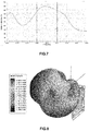
- the antenna device 1 connected to the PCB 2 and the metal plate 3 as illustrated by FIGs.2 to 4 has been simulated using the HFSSTM 3D electromagnetic tool with the dimensions of the antenna device as defined in the previous Table 1.
- the simulation results are illustrated by FIGs.5 to 8 :
Landscapes
- Engineering & Computer Science (AREA)
- Computer Networks & Wireless Communication (AREA)
- Waveguide Aerials (AREA)
Priority Applications (2)
| Application Number | Priority Date | Filing Date | Title |
|---|---|---|---|
| EP16305483.6A EP3240105A1 (de) | 2016-04-25 | 2016-04-25 | Vorrichtung mit der antennenvorrichtung |
| PCT/EP2017/059438 WO2017186581A1 (en) | 2016-04-25 | 2017-04-20 | Antenna device and apparatus including the antenna device |
Applications Claiming Priority (1)
| Application Number | Priority Date | Filing Date | Title |
|---|---|---|---|
| EP16305483.6A EP3240105A1 (de) | 2016-04-25 | 2016-04-25 | Vorrichtung mit der antennenvorrichtung |
Publications (1)
| Publication Number | Publication Date |
|---|---|
| EP3240105A1 true EP3240105A1 (de) | 2017-11-01 |
Family
ID=55854749
Family Applications (1)
| Application Number | Title | Priority Date | Filing Date |
|---|---|---|---|
| EP16305483.6A Withdrawn EP3240105A1 (de) | 2016-04-25 | 2016-04-25 | Vorrichtung mit der antennenvorrichtung |
Country Status (2)
| Country | Link |
|---|---|
| EP (1) | EP3240105A1 (de) |
| WO (1) | WO2017186581A1 (de) |
Cited By (1)
| Publication number | Priority date | Publication date | Assignee | Title |
|---|---|---|---|---|
| US11489264B2 (en) | 2018-03-21 | 2022-11-01 | Telefonaktiebolaget Lm Ericsson (Publ) | Folded antenna |
Citations (4)
| Publication number | Priority date | Publication date | Assignee | Title |
|---|---|---|---|---|
| US20120064843A1 (en) * | 2010-09-10 | 2012-03-15 | Changil Kim | Data communication device |
| US20120176278A1 (en) * | 2011-01-11 | 2012-07-12 | Merz Nicholas G L | Antenna structures with electrical connections to device housing members |
| US20140347226A1 (en) * | 2013-05-24 | 2014-11-27 | Microsoft Corporation | Back face antenna for a computing device case |
| US20160072189A1 (en) * | 2014-09-05 | 2016-03-10 | Thomson Licensing | Antenna assembly and electronic device comprising said antenna assembly |
-
2016
- 2016-04-25 EP EP16305483.6A patent/EP3240105A1/de not_active Withdrawn
-
2017
- 2017-04-20 WO PCT/EP2017/059438 patent/WO2017186581A1/en not_active Ceased
Patent Citations (4)
| Publication number | Priority date | Publication date | Assignee | Title |
|---|---|---|---|---|
| US20120064843A1 (en) * | 2010-09-10 | 2012-03-15 | Changil Kim | Data communication device |
| US20120176278A1 (en) * | 2011-01-11 | 2012-07-12 | Merz Nicholas G L | Antenna structures with electrical connections to device housing members |
| US20140347226A1 (en) * | 2013-05-24 | 2014-11-27 | Microsoft Corporation | Back face antenna for a computing device case |
| US20160072189A1 (en) * | 2014-09-05 | 2016-03-10 | Thomson Licensing | Antenna assembly and electronic device comprising said antenna assembly |
Cited By (1)
| Publication number | Priority date | Publication date | Assignee | Title |
|---|---|---|---|---|
| US11489264B2 (en) | 2018-03-21 | 2022-11-01 | Telefonaktiebolaget Lm Ericsson (Publ) | Folded antenna |
Also Published As
| Publication number | Publication date |
|---|---|
| WO2017186581A1 (en) | 2017-11-02 |
Similar Documents
| Publication | Publication Date | Title |
|---|---|---|
| US10431868B2 (en) | Antenna structure incorporated in heat spreader, heat sink, and cooling fins | |
| EP3471208B1 (de) | Dualbandantennenmodul | |
| US9735461B2 (en) | Antenna assembly for electronic device | |
| CN107078405A (zh) | 无线通信模块 | |
| US9825350B2 (en) | Assembly of circuit boards and electronic device comprising said assembly | |
| US20140139388A1 (en) | Antenna device | |
| US20190081388A1 (en) | Low-profile multi-band antenna | |
| US9985349B1 (en) | Multi-band LTE antenna | |
| US20150318616A1 (en) | Antenna apparatus | |
| CN111987466A (zh) | 一种缝隙天线和包括该缝隙天线的电子设备 | |
| EP3091608A1 (de) | Antennensystem und antennenmodul mit einem parasitären element für strahlungsmusterverbesserungen | |
| EP3240105A1 (de) | Vorrichtung mit der antennenvorrichtung | |
| JP5859064B2 (ja) | 多周波アンテナ | |
| US10135128B2 (en) | Antenna Module | |
| US20090295675A1 (en) | IC package antenna | |
| US20100149044A1 (en) | Small-sized antenna | |
| US11291145B2 (en) | Integrated antenna device | |
| US20250246816A1 (en) | Electronic device | |
| Tong et al. | Stamped metal antenna including a feeding transmission line | |
| JP2005203919A (ja) | アンテナ装置 | |
| TWI663787B (zh) | 天線結構及具有該天線結構的無線通訊裝置 | |
| Huang et al. | Effects of package structure on the patch antennas with different shapes | |
| CN206076490U (zh) | 电子装置及天线结构 | |
| TWI623147B (zh) | 天線組件及應用該天線組件之無線通訊裝置 | |
| TWI584527B (zh) | 天線結構 |
Legal Events
| Date | Code | Title | Description |
|---|---|---|---|
| PUAI | Public reference made under article 153(3) epc to a published international application that has entered the european phase |
Free format text: ORIGINAL CODE: 0009012 |
|
| AK | Designated contracting states |
Kind code of ref document: A1 Designated state(s): AL AT BE BG CH CY CZ DE DK EE ES FI FR GB GR HR HU IE IS IT LI LT LU LV MC MK MT NL NO PL PT RO RS SE SI SK SM TR |
|
| AX | Request for extension of the european patent |
Extension state: BA ME |
|
| STAA | Information on the status of an ep patent application or granted ep patent |
Free format text: STATUS: THE APPLICATION IS DEEMED TO BE WITHDRAWN |
|
| 18D | Application deemed to be withdrawn |
Effective date: 20180503 |