EP3240375B1 - Elektronikmodul mit einem ein optimiertes design aufweisenden halteelement zur verbesserten flächennutzung der leiterplatte - Google Patents
Elektronikmodul mit einem ein optimiertes design aufweisenden halteelement zur verbesserten flächennutzung der leiterplatte Download PDFInfo
- Publication number
- EP3240375B1 EP3240375B1 EP17401043.9A EP17401043A EP3240375B1 EP 3240375 B1 EP3240375 B1 EP 3240375B1 EP 17401043 A EP17401043 A EP 17401043A EP 3240375 B1 EP3240375 B1 EP 3240375B1
- Authority
- EP
- European Patent Office
- Prior art keywords
- circuit board
- printed circuit
- electronic component
- holding element
- electronic module
- Prior art date
- Legal status (The legal status is an assumption and is not a legal conclusion. Google has not performed a legal analysis and makes no representation as to the accuracy of the status listed.)
- Active
Links
Images

Classifications
-
- H—ELECTRICITY
- H05—ELECTRIC TECHNIQUES NOT OTHERWISE PROVIDED FOR
- H05K—PRINTED CIRCUITS; CASINGS OR CONSTRUCTIONAL DETAILS OF ELECTRIC APPARATUS; MANUFACTURE OF ASSEMBLAGES OF ELECTRICAL COMPONENTS
- H05K5/00—Casings, cabinets or drawers for electric apparatus
- H05K5/0026—Casings, cabinets or drawers for electric apparatus provided with connectors and printed circuit boards [PCB], e.g. automotive electronic control units
- H05K5/0047—Casings, cabinets or drawers for electric apparatus provided with connectors and printed circuit boards [PCB], e.g. automotive electronic control units having a two-part housing enclosing a PCB
- H05K5/0056—Casings, cabinets or drawers for electric apparatus provided with connectors and printed circuit boards [PCB], e.g. automotive electronic control units having a two-part housing enclosing a PCB characterized by features for protecting electronic components against vibration and moisture, e.g. potting, holders for relatively large capacitors
-
- H—ELECTRICITY
- H01—ELECTRIC ELEMENTS
- H01G—CAPACITORS; CAPACITORS, RECTIFIERS, DETECTORS, SWITCHING DEVICES, LIGHT-SENSITIVE OR TEMPERATURE-SENSITIVE DEVICES OF THE ELECTROLYTIC TYPE
- H01G2/00—Details of capacitors not covered by a single one of groups H01G4/00-H01G11/00
- H01G2/02—Mountings
- H01G2/06—Mountings specially adapted for mounting on a printed-circuit support
-
- H—ELECTRICITY
- H05—ELECTRIC TECHNIQUES NOT OTHERWISE PROVIDED FOR
- H05K—PRINTED CIRCUITS; CASINGS OR CONSTRUCTIONAL DETAILS OF ELECTRIC APPARATUS; MANUFACTURE OF ASSEMBLAGES OF ELECTRICAL COMPONENTS
- H05K3/00—Apparatus or processes for manufacturing printed circuits
- H05K3/30—Assembling printed circuits with electric components, e.g. with resistors
- H05K3/301—Assembling printed circuits with electric components, e.g. with resistors by means of a mounting structure
-
- H—ELECTRICITY
- H05—ELECTRIC TECHNIQUES NOT OTHERWISE PROVIDED FOR
- H05K—PRINTED CIRCUITS; CASINGS OR CONSTRUCTIONAL DETAILS OF ELECTRIC APPARATUS; MANUFACTURE OF ASSEMBLAGES OF ELECTRICAL COMPONENTS
- H05K7/00—Constructional details common to different types of electric apparatus
- H05K7/02—Arrangements of circuit components or wiring on supporting structure
- H05K7/12—Resilient or clamping means for holding component to structure
-
- H—ELECTRICITY
- H05—ELECTRIC TECHNIQUES NOT OTHERWISE PROVIDED FOR
- H05K—PRINTED CIRCUITS; CASINGS OR CONSTRUCTIONAL DETAILS OF ELECTRIC APPARATUS; MANUFACTURE OF ASSEMBLAGES OF ELECTRICAL COMPONENTS
- H05K2201/00—Indexing scheme relating to printed circuits covered by H05K1/00
- H05K2201/10—Details of components or other objects attached to or integrated in a printed circuit board
- H05K2201/10007—Types of components
- H05K2201/10015—Non-printed capacitor
-
- H—ELECTRICITY
- H05—ELECTRIC TECHNIQUES NOT OTHERWISE PROVIDED FOR
- H05K—PRINTED CIRCUITS; CASINGS OR CONSTRUCTIONAL DETAILS OF ELECTRIC APPARATUS; MANUFACTURE OF ASSEMBLAGES OF ELECTRICAL COMPONENTS
- H05K3/00—Apparatus or processes for manufacturing printed circuits
- H05K3/30—Assembling printed circuits with electric components, e.g. with resistors
- H05K3/32—Assembling printed circuits with electric components, e.g. with resistors electrically connecting electric components or wires to printed circuits
- H05K3/34—Assembling printed circuits with electric components, e.g. with resistors electrically connecting electric components or wires to printed circuits by soldering
- H05K3/3447—Lead-in-hole components
Definitions
- the invention relates to an electronic module (also referred to as a control unit/control device) for an actuator that can be used in a motor vehicle, in particular a clutch and/or transmission actuator, with a printed circuit board (also referred to as a PCB) and at least one electronic component arranged on the printed circuit board, wherein the electronic component is held at a distance from a surface of the printed circuit board by means of a holding element such that a receiving space is formed between the electronic component and the printed circuit board.
- Said electronic modules are used in particular as integrated local control units in corresponding drive modules of an actuator/an actuator of a motor vehicle.
- the invention consequently also relates to an actuator for actuating a clutch and/or a transmission of a motor vehicle, with such an electronic module.
- the WO 2011/050767 A1 discloses a hydrostatic actuator with a master cylinder containing a housing and a pressure chamber that can be displaced axially in the housing and is filled with pressure medium, with pressurizing pistons, with a planetary roller gear that converts a rotary drive into an axial movement, with a sleeve, a gear spindle and planetary roller bodies that roll between them, as well as with an electric motor driving the planetary roller gear with a housing-fixed stator and a rotatable rotor relative thereto, wherein the pressure chamber is ring-shaped and the planetary roller gear is arranged radially inside the pressure chamber.
- at least one sensor for acquiring operating data of the hydrostatic actuator is arranged on a printed circuit board of on-site electronics.
- a horizontal, approximately parallel alignment of a longitudinal axis of the electronic component to the printed circuit board is preferred, in particular to a vertical alignment if the most robust, durable possible Attachment of the electronic component is required on the circuit board.
- the electronic components are to be supported in particular against vibrations occurring during operation.
- these are usually glued directly onto the surface of the printed circuit board.
- this attachment method has the disadvantage that a relatively large surface area of the printed circuit board, on which the component is glued, cannot be used.
- the electronic component is held at a distance from a surface of the printed circuit board by means of a holding element such that a receiving space is formed between the electronic component and the printed circuit board.
- the holding element thus serves as a spacer which is shaped, for example recessed, in sections, namely in the area of the receiving space, in such a way that it is held in place between the printed circuit board and the electronic component.
- the usable surface of the circuit board is significantly increased.
- additional components such as flat chips (such as microcontrollers, sensors, etc.) or passive SMD components can now be provided below the electronic component on the printed circuit board, ie in the receiving space, by means of this holding element.
- the electronic component has an elongate shape/external shape, preferably a cylindrically extending shape/external shape, and/or is attached lying to the printed circuit board. Lying here means that position defined by an angle between (inclusive) 0° (parallel) and 45° between its longitudinal axis of the electronic component and the surface/a reference plane lying in the surface of the printed circuit board. This angle is particularly preferably 0°, i.e. the electronic component is aligned with its longitudinal axis parallel to the surface/reference plane in the surface of the printed circuit board. This horizontal arrangement in particular significantly reduces the vibration load during operation of the electronic module in a motor vehicle.
- the electronic component as provided according to the invention, is designed as an electrolytic capacitor, the implementation according to the invention works particularly efficiently.
- the electronic component is attached to the holding element in a form-fitting manner, the component can be fixed particularly quickly to the printed circuit board.
- the electronic component is held by pretensionable holding lugs (also referred to as clip projections/snap-in lugs) that are attached/formed to the holding element.
- the electronic component is held stable in the fastened state by the pretension.
- the electronic component is held/clamped in the holding element without play. As a result, the electronic component is fixed even more stably in relation to vibration loads.
- the holding element has a preferably box-shaped, approximately polygonal, more preferably rectangular, frame structure which encloses a window area (also referred to as a through-opening) within which the electronic component is at least partially arranged. This allows a particularly large area of the circuit board can be used towards the electronic component.
- the holding element has at least one support foot, preferably several, for example three or four support feet, with which it is/are anchored in the printed circuit board.
- the design of such support feet means that a particularly large area of the printed circuit board can be used during operation.
- these support feet are a direct part of the frame structure, i.e. they are connected to the frame structure as a single piece of material. This further simplifies the construction of the holding element.
- the support feet are advantageously anchored/fastened in the printed circuit board by means of a plurality of fastening elements, for example by means of pins/locking bolts or snap-on projections. As a result, the vibration load on the electronic component during operation can be further reduced.
- the electronic component is connected to a housing of the electronic module via a thermally conductive adhesive connection. This improves the dissipation of excess heat from the electronic component.
- the holding element is formed from a plastic material, preferably a plastic material that can be processed by injection molding, i.e. is more preferably designed as a component produced by injection molding. As a result, the holding element can be manufactured particularly efficiently.
- the invention also relates to an actuator for actuating a clutch and/or a transmission, ie a clutch and/or transmission actuator, of a motor vehicle, such as a car, truck, bus or agricultural vehicle, with an electronic module according to at least one of the versions described above.
- a clutch and/or transmission actuator of a motor vehicle, such as a car, truck, bus or agricultural vehicle
- an electronic module according to at least one of the versions described above.
- an actuator is also designed to be particularly durable overall.
- fastening clips prefferably also possible for the fastening clips to have undercuts.
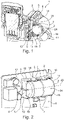
- an electronic module 1 according to the invention is shown according to a preferred exemplary embodiment.
- the electronics module 1 is designed as a control unit/control unit of an actuator, namely a clutch and/or transmission actuator.
- the electronics module 1 is consequently electrically connected to a drive unit of the actuator during operation.
- the electronics module 1 preferably has means, not shown here for the sake of clarity, for driving the actuator and/or for energizing a sensor device for detecting a position (rotational position) of an actuating element (rotor and/or spindle shaft) of the actuator.
- the electronic module 1 is thus designed during operation as a local control unit integrated in the actuator.
- the electronics module 1 typically has a housing 11 in which a printed circuit board 2 is accommodated.
- This printed circuit board 2 in the form of a printed circuit board/PCB has a number of electronic components and conductor tracks in order to form a corresponding switching structure.
- an electronic component 3 is attached to the printed circuit board 2 .
- This electronic component 3 is designed as a capacitor component in the form of an electrolytic capacitor.
- the electronic component 3 is therefore also referred to as a capacitor component 3 below.
- the capacitor component 3 has a cylindrical outer shape.
- the capacitor component 3 is arranged lying on the printed circuit board 2, i.e. with its longitudinal axis 25 aligned essentially parallel to a surface 6 of the printed circuit board 2 that extends/flat in an imaginary reference plane.
- the arrangement of the capacitor component 3 is also particularly good in 2 recognizable as a whole.
- a connecting line 12 which opens into the capacitor component 3 is electrically connected to further electronic components in a typical manner. Since the capacitor component 3 has an essentially round, namely circular, cross-sectional shape, the connecting line 12 is connected in a middle/central area of an end face 19 of the capacitor component 3 .
- Another connecting line 12, not shown for the sake of clarity, is connected to another end face of the capacitor component 3 in the same way.
- This type of construction and double-sided axial cathode/anode arrangement is very common with well-known electrolytic capacitor manufacturers and in particular has a clear commercial advantage over other conventional forms and arrangements in terms of connections. This design is preferred because of its inherently low cost.
- the capacitor component 3 is not fixed directly in contact with the printed circuit board 2/the surface 6 of the printed circuit board 2, but is fixed at a distance from the surface 6 of the printed circuit board 2 by means of a holding element 4.
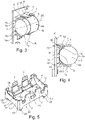
- This spaced-apart position of the capacitor component 3 in an assembled state of the assembly of circuit board 2, holding element 4 and capacitor component 3 is also particularly good in the Figs. 3 and 4 recognizable.
- the capacitor component 3 is held at a distance from the surface 6 by means of the holding element 4 such that a receiving space 5 is formed between the flat surface 6 and the capacitor component 3, ie an underside 13 of the capacitor component 3 which faces the surface 6. Additional electronic components, not shown here for the sake of clarity, are placed in this receiving space 5 .
- the holding element 4 is designed in figure 5 clearly visible.
- the holding element 4 is provided with a window area 9 which forms a through opening. This window area 9 is enclosed by a box-shaped/rectangular frame structure 8 of the holding element 4 .
- the holding element 4 essentially has four sides which run perpendicularly or parallel to one another, forming a rectangle.
- Two opposing longitudinal sides 14 of the holding element 4 have several, namely two, holding lugs 7 each.
- the retaining lugs 7 form snap-in lugs/clips projections which are elastically deformable and are pressed resiliently against the outside/lateral surface 18 of the capacitor component 3 in the fastened state. In particular, these holding lugs 7 limit the movement of the capacitor component 3 away from the printed circuit board 2.
- the capacitor component 3 can thus be seen during operation due to the elastic prestressing of the retaining lugs 7 between the support projections 16 / the retaining webs 15 and the retaining lugs 7 clamped.
- the lateral surface 18 of the capacitor component 3 is encompassed in a form-fitting manner.
- the capacitor component 3 is arranged within the frame structure 8 at a distance from the printed circuit board.
- the transverse sides 17 in turn serve to support the end faces 19 of the capacitor component 3.
- the holding element 4 has a supporting foot 10 in each of its corner regions, ie in its transition regions between the longitudinal and transverse sides 14 and 17 .
- a total of four supporting feet 10 are therefore arranged on the holding element 4 .
- the support feet 10 are arranged on an underside 20 of the holding element 4 and extend away from the lower edges 21 of the longitudinal sides 14 and transverse sides 17 or of the holding web 15 .
- the support feet 10 form a support plane 22 as a whole, which, in the fastened state, lies parallel to the surface 6, namely over a large area directly on the surface 6.
- the lower edges 21 are arranged at a distance from the printed circuit board 2 .
- the longitudinal and transverse sides 14 and 15 are also partially arranged at a distance from the printed circuit board 2, so that the receiving space 5 is in turn expanded by these cavities additionally created as a result.
- a fastening element 23 is inserted in each of the supporting feet 10 to fasten the holding element 4 or the supporting feet 10 .
- Each of these fastening elements 23 is preferably embodied as a plug which is then inserted/snapped in a form-fitting manner in a receiving bore/receiving hole in the printed circuit board 2 .
- the holding element 4 is connected to the printed circuit board 2 via a plug connection.
- the holding element 4 is preferably made of a plastic material (such as a dielectric) as a whole.
- the holding element 4 is produced by means of an injection molding process.
- the longitudinal sides 14 together with the holding webs 15, the transverse sides 17 and the support feet 10 are consequently all made of one piece of material.
- the fastening elements 23 can in turn also be designed in one piece with the support feet 10, but can alternatively also be manufactured as separate components.
- the capacitor component 3 is additionally fastened/fixed to the housing 11 by means of a thermally conductive adhesive connection (not shown in detail for the sake of clarity).
- a thermally conductive adhesive connection (not shown in detail for the sake of clarity).
- an adhesive bead is preferably arranged on an upper side 24 of the capacitor component 3 facing away from the printed circuit board 2, which adhesively connects the capacitor component 3 and the housing 11 to one another.
- This adhesive connection is then preferably applied in a heat sink in the lateral surface 18 of the capacitor component 3 .
- the holding element 4 When the electronic module 1 is assembled, the holding element 4 is first applied to the printed circuit board 2 .
- the holding element 4 is latched with its fastening elements 3 in fastening means receiving holes/through-holes in the printed circuit board 2 and thus anchored in the printed circuit board 2 in a form-fitting manner.
- the capacitor component 3 is again clipped into the holding element 4 .
- the capacitor component 3 is pre-aligned essentially parallel to the printed circuit board 2 and pushed into the window area 9 of the frame structure 8, under elastic prestressing of the retaining lugs 7, until the retaining lugs 7 hold the capacitor component 3 in the direction of the printed circuit board 2 due to their elastic forces.
- the retaining lugs 7 engage behind the capacitor component 3 and hold the capacitor component 3 in a prestressed position, with the capacitor component 3 being pressed against the retaining webs 15 at the same time.
- the housing 11 is then fastened around the assembly between the printed circuit board 2 and the capacitor component 3 (including the retaining element 4), so that the printed circuit board 2 is accommodated in the housing 11 in a non-displaceable manner.
- the thermally conductive adhesive connection between the capacitor component 3 and the housing 11 is preferably also applied.
- the electronic module 1 has a holding element 4 for fastening electrolytic capacitors 3 with partial holding in the bottom area (fastening elements 23) and flexible clip holders (holding lugs 7), which prestress the component 3 in the holder. Cutouts in the bottom area (window area 9) of the holding element 4 are provided in order to be able to allow component placement on the PCB 2 in the area.
- the holding part / Retaining element 4 is preferably designed as a part injection molded from plastic. The capacitor 3 is clipped into the holding part 4 and the clips 7 of the holding part 4 ensure the pretension between the clip geometry on the side and the raised contact surfaces (support projections 16) on the bottom of the part 4.
Landscapes
- Engineering & Computer Science (AREA)
- Microelectronics & Electronic Packaging (AREA)
- Power Engineering (AREA)
- Manufacturing & Machinery (AREA)
- Structures For Mounting Electric Components On Printed Circuit Boards (AREA)
- Mounting Components In General For Electric Apparatus (AREA)
Description
- Die Erfindung betrifft ein Elektronikmodul (auch als Steuereinheit / Steuergerät bezeichnet) für einen in einem Kraftfahrzeug verwendbaren Aktor, insbesondere einem Kupplungs- und/oder Getriebeaktor, mit einer Leiterplatte (auch als PCB bezeichnet) sowie zumindest einem auf der Leiterplatte angeordneten elektronischen Bauteil, wobei das elektronische Bauteil mittels eines Halteelementes so beabstandet zu einer Oberfläche der Leiterplatte gehalten ist, dass ein Aufnahmeraum zwischen dem elektronischen Bauteil und der Leiterplatte ausgebildet ist. Besagte Elektronikmodule werden insbesondere als integrierte lokale Steuereinheiten in entsprechenden Antriebsmodulen einer Aktorik / eines Aktors eines Kraftfahrzeuges verwendet. Die Erfindung betrifft folglich auch einen Aktor zum Betätigen einer Kupplung und/oder eines Getriebes eines Kraftfahrzeuges, mit einem solchen Elektronikmodul.
- Prinzipiell sind Elektronikmodule zur Erfassung von Betriebsdaten einer Antriebseinheit eines Aktors und/oder zur Steuerung der Antriebseinheit bereits bekannt. Die
WO 2011/050767 A1 offenbart einen Hydrostat-Aktor mit einem Geberzylinder enthaltend ein Gehäuse und eine in dem Gehäuse axial verlagerbaren, eine mit Druckmittel befüllte Druckkammer mit druckbeaufschlagenden Kolben, mit einem einen Drehantrieb in eine Axialbewegung wandelnden Planetenwälzgetriebe, mit einer Hülse, einer Getriebespindel und zwischen diesen abwälzenden Planetenwälzkörpern sowie mit einem das Planetenwälzgetriebe antreibenden Elektromotor mit einem gehäusefest verbundenen Stator und einem gegenüber diesem verdrehbaren Rotor, wobei die Druckkammer ringförmig ausgebildet ist und das Planetenwälzgetriebe radial innerhalb der Druckkammer angeordnet ist. Auf einer Platine einer Vorortelektronik ist in diesem Zusammenhang zumindest ein Sensor zur Erfassung von Betriebsdaten des Hydrostat-Aktors angeordnet. - Bei der Verwendung relativ großvolumiger, schwerer elektronischer Bauteile, wie Kondensatorbauteilen, auf Leiterplatten wird eine liegende, etwa eine parallele Ausrichtung einer Längsachse des elektronischen Bauteils zur Leiterplatte, insbesondere dann einer stehenden Ausrichtung vorgezogen, wenn eine möglichst robuste, dauerfeste Anbringung des elektronischen Bauteils an der Leiterplatte gefordert ist. Die elektronischen Bauteile sind hierbei insbesondere gegenüber im Betrieb auftretenden Vibrationen abzustützen. Um das elektronische Bauteil ausreichend fest an der Leiterplatte zu befestigen, werden diese zumeist unmittelbar auf die Oberfläche der Leiterplatte aufgeklebt. Diese Befestigungsmethode hat jedoch wiederum den Nachteil, dass ein relativ großer Flächenbereich der Leiterplatte, auf dem das Bauteil aufgeklebt wird, nicht genutzt werden kann.
- Alternative Befestigungsmöglichkeiten, um Bauteile mittels Abstandselementen auf der Leiterplatte von derselben zu beabstanden sind bekannt, z.B. aus der
DE 100 62 962 A1 ,US 2008/291653 A1 ,US 2011/038133 A1 ,JP 2006 148011 A DE 198 14 156 C1 oder derWO 2013/002684 A1 . Auch hier kann es zu Problemen bei der Wärmeabfuhr des elektronischen Bauteils kommen. - Es ist daher die Aufgabe der vorliegenden Erfindung, die aus dem Stand der Technik bekannten Nachteile zu beheben und eine Leiterplatte für ein Elektronikmodul zur Verfügung zu stellen, bei der die Bauraumausnutzung gesteigert werden soll.
- Dies wird erfindungsgemäß mittels der Merkmalskombination, wie sie im Anspruch 1 beansprucht ist, gelöst. Das elektronische Bauteil ist mittels eines Halteelementes so beabstandet zu einer Oberfläche der Leiterplatte gehalten ist, dass ein Aufnahmeraum zwischen dem elektronischen Bauteil und der Leiterplatte ausgebildet ist. Das Haltelement dient somit als Abstandshalter, der abschnittsweise, nämlich im Bereich des Aufnahmeraums, so ausgeformt, etwa ausgespart, ist, dass zwischen der Leiterplatte und dem elektronischen Bauteil vorgehalten ist.
- Durch das beabstandete Anbringen des elektronischen Bauteils zur Leiterplatte mittels des Halteelementes wird die nutzbare Oberfläche der Leiterplatte deutlich erhöht. Insbesondere können durch dieses Halteelement nun zusätzliche Bauteile, etwa flache Chips (wie z.B. Mikrokontroller, Sensoren etc.) oder passive SMD Bauteile unterhalb des elektronischen Bauteils auf der Leiterplatte, d.h. im Aufnahmeraum, vorgesehen werden.
- Weitere vorteilhafte Ausführungsformen sind in den Unteransprüchen beansprucht und nachfolgend näher erläutert.
- Weiterhin ist es vorteilhaft, wenn das elektronische Bauteil eine längliche Form / Außenform, vorzugsweise eine sich zylindrisch erstreckende Form / Außenform, aufweist und/oder liegend zur Leiterplatte angebracht ist. Unter liegend ist hierbei jene Position zu verstehen, die durch einen zwischen seiner Längsachse des elektronischen Bauteils und der Oberfläche / einer in der Oberfläche liegenden Bezugsebene der Leiterplatte eingeschlossenen Winkel definiert ist, der zwischen (einschließlich) 0° (parallel) und 45° beträgt. Besonders bevorzugt beträgt dieser Winkel 0°, d.h. ist das elektronische Bauteil mit seiner Längsachse parallel zu der Oberfläche / Bezugsebene in der Oberfläche der Leiterplatte ausgerichtet. Durch diese liegende Anordnung wird insbesondere die Vibrationsbelastung während des Betriebes des Elektronikmoduls in einem Kraftfahrzeug deutlich reduziert.
- Ist das elektronische Bauteil, wie erfindungsgemäß vorgesehen als Elektrolytkondensator ausgestaltet, ist die erfindungsgemäße Umsetzung besonders effizient wirkend.
- Ist das elektronische Bauteil formschlüssig an dem Halteelement angebracht, ist eine besonders rasche Fixierung des Bauteils an der Leiterplatte möglich.
- In diesem Zusammenhang ist es weiterhin vorteilhaft, wenn das elektronische Bauteil über an dem Halteelement angebrachte / ausgebildete vorspannbare Haltenasen (auch als Clips-Vorsprünge / Schnappnasen bezeichnet) gehalten ist. Durch die Vorspannung ist das elektronische Bauteil im befestigten Zustand stabil gehalten.
- Auch ist es zweckmäßig, wenn das elektronische Bauteil spielfrei in dem Halteelement gehalten / eingespannt ist. Dadurch ist das elektronische Bauteil noch stabiler gegenüber Vibrationsbelastungen fixiert.
- Von Vorteil ist es zudem, wenn das Halteelement eine, vorzugsweise kastenförmige, etwa polygonförmige, weiter bevorzugt rechteckförmige, Rahmenstruktur aufweist, die einen Fensterbereich (auch als Durchgangsöffnung bezeichnet) einschließt, innerhalb der das elektronische Bauteil zumindest teilweise angeordnet ist. Dadurch kann ein besonders großer Bereich der Leiterplatte hin zu dem elektronischen Bauteil ausgenutzt werden.
- In diesem Zusammenhang ist es weiterhin zweckmäßig, wenn das Halteelement zumindest einen Stützfuß, vorzugweise mehrere, etwa drei oder vier Stützfüße aufweist, mit dem / denen es in der Leiterplatte verankert ist. Durch die Ausbildung solcher Stützfüße ist eine besonders große Fläche der Leiterplatte im Betrieb ausnutzbar.
- Weiter bevorzugt sind diese Stützfüße direkter Bestandteil der Rahmenstruktur, d.h. stoffeinteilig mit der Rahmenstruktur verbunden. Dadurch wird der Aufbau des Halteelementes weiter vereinfacht.
- Die Stützfüße sind vorteilhafterweise mittels mehrerer Befestigungselemente, etwa mittels Pins / Steckbolzen oder Schnappvorsprüngen in der Leiterplatte verankert / befestigt. Dadurch lässt sich die Vibrationsbelastung auf das elektronische Bauteil im Betrieb weiter verringern.
- Desweiteren ist es erfindungsgemäß vorgesehen, dass das elektronische Bauteil über eine wärmeleitende Klebeverbindung mit einem Gehäuse des Elektronikmoduls verbunden ist. Dadurch wird die Abfuhr überschüssiger Wärme aus dem elektronischen Bauteil verbessert.
- Zudem ist es vorteilhaft, wenn das Halteelement aus einem Kunststoffmaterial, vorzugsweise einem spritzgießtechnisch verarbeitbaren Kunststoffmaterial, ausgeformt ist, d.h. weiter bevorzugt als ein spritzgusstechnisch hergestelltes Bauteil ausgebildet ist. Dadurch lässt sich das Halteelement besonders effizient fertigen.
- Die Erfindung betrifft desweiteren einen Aktor zum Betätigen einer Kupplung und/oder eines Getriebes, d.h. einen Kupplungs- und/oder Getriebeaktor, eines Kraftfahrzeuges, wie eines Pkws, Lkws, Busses oder landwirtschaftlichen Nutzfahrzeuges, mit einem Elektronikmodul nach zumindest einem der zuvor bezeichneten Ausführungen. Dadurch ist auch ein Aktor gesamtheitlich besonders langlebig ausgestaltet.
- Auch wird ein Verfahren zum Zusammenbau eines Elektronikmoduls für einen Aktor, mit zumindest folgenden Schritten offenbart:
- a) Befestigen eines Halteelementes auf einer Leiterplatte, und
- b) Befestigen eines elektronischen Bauteils, vorzugsweise eines Elektrolytkondensators, in einer liegenden Ausrichtung an dem Halteelement, derart, dass ein Aufnahmeraum zwischen einer Oberfläche der Leiterplatte und einer der Leiterplatte zugewandten Seite des elektronischen Bauteils ausgestaltet wird.
- In anderen Worten ausgedrückt, ist somit ein Befestigungselement (Halteelement) für elektrolytische Kondensatoren umgesetzt, um einen zusätzlichen Bauraum unterhalb des Kondensators zu erreichen. Der Elektrolytkondensator ist aus Stabilitätsgründen vorzugsweise parallel zur PCB (Leiterplatte) angeordnet. Das Befestigungselement kann mit einer Steckverbindung mit der PCB und/oder vorgespannten Clips zum Halten des Kondensators gegen Vibrationen in Position gebracht werden. Das Befestigungselement weist einen offenen Boden auf, der parallel zu der PCB verläuft, jedoch zur PCB beabstandet ist. Auf diese Weise kann die zusätzliche Fläche unterhalb des Kondensators effektiv genutzt werden. Zum besseren Kühlen des Elektrolytkondensators weist dieser einen in axialer Richtung gesehenen rückwärtigen Bereich auf, der mit einer Wärmesenke ausgeführt ist. Die Wärmesenke ist über einen Wärmekleber weiter mit dem Gehäuse des Elektronikmoduls verbunden.
- Desweiteren ist es alternativ auch möglich, dass die Befestigungsclips Hinterschnitte aufweisen.
- Die Erfindung wird nun nachfolgend anhand von Figuren näher erläutert.
- Es zeigen:
- Fig. 1
- eine perspektivische Darstellung eines geschnitten dargestellten, erfindungs-gemäßen Elektronikmoduls nach einem bevorzugten Ausführungsbeispiel, wo-bei die Schnittebene derart gewählt ist, dass die Anbringung eines elektroni-schen Bauteils mittels eines Halteelementes an einer Leiterplatte gut zu erken-nen ist,
- Fig. 2
- eine perspektivische Darstellung eines Teils des in dem Elektronikmodul nach
Fig. 1 eingesetzten Zusammenbaus aus der Leiterplatte und dem elektroni-schen Bauteil, wobei die Anbringung des elektronischen Bauteils mittels des Halteelementes gut zu erkennen ist, - Fig. 3
- eine perspektivische Darstellung des Zusammenbaus aus Leiterplatte und elektronischem Bauteil nach
Fig. 2 , wobei der Zusammenbau derart geschnit-ten ist, dass das elektronische Bauteil quer zu seiner Längsachse geschnitten ist, sodass die beabstandete Haltung des elektronischen Bauteils ersichtlich ist, - Fig. 4
- eine Querschnittsdarstellung des in
Fig. 3 geschnitten abgebildeten Zusam-menbaus aus Leiterplatte und elektronischem Bauteil, - Fig. 5
- eine perspektivische Darstellung einer im Zusammenbau der Leiterplatte ab-gewandten Oberseite eines Halteelementes, wie es in den
Fign. 1 bis 4 ein-gesetzt ist, zur Befestigung des elektronischen Bauteils, - Fig. 6
- eine perspektivische Darstellung des Halteelementes nach
Fig. 5 von seiner Unterseite, an der Befestigungselemente zur Verankerung in der Leiterplatte gut erkennbar sind, und - Fig. 7
- eine Querschnittsdarstellung des Halteelementes nach den
Fign. 5 und6 , so-dass besonders gut der Querschnitt der Haltenasen sowie ein das elektroni-sche Bauteil hin zur Leiterplatte abstützender Haltesteg veranschaulicht sind. - Die Figuren sind lediglich schematischer Natur und dienen ausschließlich dem Verständnis der Erfindung. Die gleichen Elemente sind mit denselben Bezugszeichen versehen.
- In
Fig. 1 ist ein erfindungsgemäßes Elektronikmodul 1 nach einem bevorzugten Ausführungsbeispiel dargestellt. Das Elektronikmodul 1 ist als eine Steuereinheit / ein Steuergerät eines Aktors, nämlich eines Kupplungs- und/oder Getriebeaktors, ausgebildet. Das Elektronikmodul 1 ist folglich im Betrieb mit einer Antriebseinheit des Aktors elektrisch verbunden. Das Elektronikmodul 1 weist vorzugsweise hier der Übersichtlichkeit nicht dargestellte Mittel zum Antrieb des Aktors und/oder zum Bestromen einer Sensoreinrichtung zur Erfassung einer Stellung (Drehstellung) eines Stellelementes (Rotors und/oder Spindelwelle) des Aktors auf. Das Elektronikmodul 1 ist somit im Betrieb als eine im Aktor integrierte lokale Steuereinheit ausgebildet. - Das Elektronikmodul 1 weist auf typische Weise ein Gehäuse 11 auf, in dem eine Leiterplatte 2 aufgenommen ist. Diese Leiterplatte 2 in Form eines printed circuit boards / einer PCB weist mehrere elektronische Bauteile sowie Leiterbahnen auf, um eine entsprechende Schaltstruktur auszubilden. Unter anderem ist auf der Leiterplatte 2 ein elektronisches Bauteil 3 befestigt. Dieses elektronische Bauteil 3 ist als Kondensatorbauteil in Form eines Elektrolytkondensators ausgestaltet. Das elektronische Bauteil 3 ist daher nachfolgend auch als Kondensatorbauteil 3 bezeichnet. Das Kondensatorbauteil 3 weist eine zylindrische Außenform auf. Das Kondensatorbauteil 3 ist liegend auf der Leiterplatte 2 angeordnet, d.h. mit seiner Längsachse 25 im Wesentlichen parallel zu einer sich in einer gedachten Bezugsebene erstreckenden / ebenen Oberfläche 6 der Leiterplatte 2 ausgerichtet.
- Die Anordnung des Kondensatorbauteils 3 ist auch besonders gut in
Fig. 2 gesamtheitlich zu erkennen. Eine in das Kondensatorbauteil 3 einmündende Verbindungsleitung 12 ist auf typische Weise elektrisch mit weiteren elektronischen Bauteilen weiter verbunden. Da das Kondensatorbauteil 3 eine im Wesentlichen runde, nämlich kreisrunde Querschnittsform aufweist, ist die Verbindungsleitung 12 in einem mittigen / zentralen Bereich einer Stirnseite 19 des Kondensatorbauteils 3 angeschlossen. Eine weitere der Übersichtlichkeit nicht dargestellte Verbindungsleitung 12 ist an einer anderen Stirnseite des Kondensatorbauteils 3 auf gleiche Weise angeschlossen. Diese Bauform und beidseitige axiale Kathode/ Anode-Anordnung sind sehr häufig bei bekannten Elektrolytenkondensator-Herstellern und hat insbesondere einen deutlichen kommerziellen Vorteil vor anderen konventionellen Bauformen und Anordnungen in puncto der Anschlüsse. Diese Bauform ist wegen der ihr eigenen niedrigen Kosten bevorzugt. - Erfindungsgemäß ist das Kondensatorbauteil 3 nicht direkt, unter Kontakt mit der Leiterplatte 2 / der Oberfläche 6 der Leiterplatte 2 fixiert, sondern mittels eines Halteelementes 4 beabstandet zu der Oberfläche 6 der Leiterplatte 2 befestigt. Diese beabstandete Stellung des Kondensatorbauteils 3 in einem zusammengebauten Zustand des Zusammenbaus aus Leiterplatte 2, Halteelement 4 und Kondensatorbauteil 3 ist auch besonders gut in den
Fign. 3 und 4 erkennbar. Das Kondensatorbauteil 3 ist mittels des Halteelementes 4 derart beabstandet zu der Oberfläche 6 gehalten, dass sich ein Aufnahmeraum 5 zwischen der ebenen Oberfläche 6 und dem Kondensatorbauteil 3, d.h. einer Unterseite 13 des Kondensatorbauteils 3, die der Oberfläche 6 zugewandt ist, ausbildet. In diesem Aufnahmeraum 5 sind weitere, hier der Übersichtlichkeit halber nicht dargestellte, elektronische Bauteile platziert. - Das Halteelement 4 ist in seiner Ausbildung in
Fig. 5 gut zu erkennen. Das Halteelement 4 ist mit einem Fensterbereich 9 versehen, der eine Durchgangsöffnung bildet. Dieser Fensterbereich 9 ist durch eine kastenförmige / rechteckförmige Rahmenstruktur 8 des Halteelementes 4 eingeschlossen. Das Halteelement 4 weist im Wesentlichen vier Seiten auf, die senkrecht bzw. parallel, unter Ausbildung eines Rechteckes, zueinander verlaufen. Zwei sich gegenüberliegende Längsseiten 14 des Halteelementes 4 weisen mehrere, nämlich jeweils zwei Haltenasen 7 auf. Die Haltenasen 7 bilden Schnappnasen / Clips-Vorsprünge aus, die elastisch verformbar sind und im befestigten Zustand federelastisch an die Außenseite / Mantelfläche 18 des Kondensatorbauteils 3 angedrückt sind. Insbesondere beschränken diese Haltenasen 7 die Bewegung des Kondensatorbauteils 3 weg von der Leiterplatte 2. Hin zu der Leiterplatte 2 ist das Kondensatorbauteil 3 über zwei Haltestege 15 abgestützt. Jede Längsseite 14 bildet dabei über ihre gesamte Länge hinweg einen Haltesteg 15 aus. Die Haltestege 15 erstrecken sich somit, wie bereits die Längsseiten 14, parallel zueinander. Diese Haltestege 15 definieren eine Auflage des Kondensatorbauteils 3 zur Leiterplatte 2 hin. An jedem Haltesteg 15 sind mehrere Auflagevorsprünge 16 vorgesehen. Jeder Haltesteg 15 weist drei Auflagevorsprünge 16 auf. Senkrecht zu den Längsseiten 14 sind zwei Querseiten 17 gegenüberliegend angeordnet, die die Längsseiten 14 miteinander verbinden. - Wie wiederum in
Fig. 4 erkennbar, ist somit das Kondensatorbauteil 3 im Betrieb durch die elastische Vorspannung der Haltenasen 7 zwischen den Auflagevorsprüngen 16 / den Haltestegen 15 und den Haltenasen 7 eingespannt. Dadurch ist insbesondere die Mantelfläche 18 des Kondensatorbauteils 3 formschlüssig umgriffen. Das Kondensatorbauteil 3 ist innerhalb der Rahmenstruktur 8 beabstandet zur Leiterplatte angeordnet. Zur Abstützung der Stirnseiten 19 des Kondensatorbauteils 3 dienen wiederum die Querseiten 17. - In
Fig. 6 ist dargestellt, dass das Halteelement 4 an seinen Eckenbereichen, d.h. an seinen Übergangsbereichen zwischen den Längs- und Querseiten 14 und 17, jeweils einen Stützfuß 10 aufweist. Somit sind insgesamt vier Stützfüße 10 an dem Halteelement 4 angeordnet. Die Stützfüße 10 sind an einer Unterseite 20 des Halteelementes 4 angeordnet und erstrecken sich von den Unterkanten 21 der Längsseiten 14 und Querseiten 17 bzw. des Haltesteges 15 weg. Dadurch bilden die Stützfüße 10 gesamtheitlich eine Auflageebene 22 aus, die im befestigten Zustand parallel zur Oberfläche 6, nämlich flächig direkt auf der Oberfläche 6, aufliegt. Des Weiteren sind die Unterkanten 21 beabstandet zur Leiterplatte 2 angeordnet. Dadurch sind die Längs- und Querseiten 14 und 15 teilweise ebenfalls beabstandet zu der Leiterplatte 2 angeordnet, sodass der Aufnahmeraum 5 wiederum durch diese dadurch zusätzlich erzeugten Hohlräume erweitert ist. - Zur Befestigung des Halteelementes 4 bzw. der Stützfüße 10 ist in jedem der Stützfüße 10 ein Befestigungselement 23 eingesetzt. Jedes dieser Befestigungselemente 23 ist vorzugsweise als ein Stecker ausgebildet, der dann formschlüssig in einer Aufnahmebohrung / einem Aufnahmeloch der Leiterplatte 2 eingeschoben ist / eingerastet ist. Somit ist das Halteelement 4 über eine Steckverbindung mit der Leiterplatte 2 verbunden.
- Wie hierbei auch besonders gut in
Fig. 7 erkennbar, ist das Halteelement 4 gesamtheitlich vorzugsweise aus einem Kunststoffmaterial (etwa einem Dielektrikum) gefertigt. Das Halteelement 4 ist mittels eines Spritzgussverfahrens hergestellt. Die Längsseiten 14 samt Haltestegen 15, die Querseiten 17 sowie die Stützfüße 10 sind folglich allesamt miteinander stoffeinteilig ausgebildet. Die Befestigungselemente 23 können wiederum ebenfalls stoffeinteilig mit den Stützfüßen 10 ausgestaltet sein, können alternativ jedoch auch als separate Bauteile gefertigt sein. - Zurückkommend auf
Fig. 1 sei auch darauf hingewiesen, dass das Kondensatorbauteil 3 im vollständig zusammengebauten Zustand des Elektronikmoduls 1 zusätzlich mittels einer der Übersichtlichkeit halber nicht weiter dargestellten wärmeleitfähigen Klebeverbindung an dem Gehäuse 11 befestigt / fixiert ist. Hierfür ist vorzugsweise eine Klebewulst auf einer der Leiterplatte 2 abgewandten Oberseite 24 des Kondensatorbauteils 3 angeordnet, die das Kondensatorbauteil 3 sowie das Gehäuse 11 adhäsiv miteinander verbindet. Vorzugsweise ist diese Klebeverbindung dann in einer Wärmesenke in der Mantelfläche 18 des Kondensatorbauteils 3 angebracht. - Bei einem Zusammenbau des Elektronikmoduls 1 wird zunächst das Halteelement 4 auf die Leiterplatte 2 aufgebracht. Hierfür wird das Halteelement 4 mit seinen Befestigungselementen 3 in Befestigungsmittelaufnahmelöchern / Durchgangslöchern in der Leiterplatte 2 eingerastet und somit formschlüssig in der Leiterplatte 2 verankert. Im Anschluss daran wird das Kondensatorbauteil 3 wiederum in das Halteelement 4 eingeclipst. Hierzu wird das Kondensatorbauteil 3 im Wesentlichen parallel zur Leiterplatte 2 vorausgerichtet und soweit in den Fensterbereich 9 der Rahmenstruktur 8, unter elastischer Vorspannung der Haltenasen 7 hineingedrückt, bis die Haltenasen 7 aufgrund ihrer elastischen Kräfte das Kondensatorbauteil 3 in Richtung Leiterplatte 2 festhalten. Wenn schließlich der dickste Bereich der Mantelfläche 18 zur Leiterplatte hin an den Haltenasen 7 vorbeigeschoben ist, rasten die Haltenasen 7 hinter dem Kondensatorbauteil 3 ein und halten das Kondensatorbauteil 3 in einer vorgespannten Stellung, wobei das Kondensatorbauteil 3 zugleich an den Haltestegen 15 angedrückt wird. Im Anschluss daran wird das Gehäuse 11 fertig um den Zusammenbau zwischen Leiterplatte 2 und Kondensatorbauteil 3 (inkl. Halteelement 4) herum befestigt, sodass die Leiterplatte 2 verschiebefest in dem Gehäuse 11 aufgenommen ist. Bei diesem Schritt wird dabei vorzugsweise auch die wärmeleitende Klebeverbindung zwischen Kondensatorbauteil 3 und Gehäuse 11 angebracht.
- In anderen Worten ausgedrückt, ist in dem erfindungsgemäßen Elektronikmodul 1 ein Halteelement 4 für die Befestigung von Elektrolytkondensatoren 3 mit partieller Halterung im Bodenbereich (Befestigungselemente 23) sowie flexiblen Kliphaltern (Haltenasen 7), die das Bauteil 3 in der Halterung vorspannen, vorgesehen. Ausschnitte im Bodenbereich (Fensterbereich 9) des Halteelements 4 sind vorgesehen, um die Bauteilplatzierung auf dem PCB 2 in dem Bereich zulassen zu können. Das Halteteil / Halteelement 4 ist vorzugsweise als ein aus Kunststoff gespritztes Teil konzipiert. Der Kondensator 3 wird in dem Halteteil 4 eingeklipst und die Klipse 7 des Halteteils 4 sorgen dabei für die Vorspannung zwischen der Klippgeometrie seitlich und den erhobenen Kontaktflächen (Auflagevorsprünge 16) auf dem Boden des Teils 4. Somit ist der Elektrolytkondensator 3 vibrationsfest gehalten. Das Halteteil 4 an sich ist durch Pins 23 in der PCB 2 in x/y Richtung (in der Ebene der PCB 2) befestigt und in der axialen z- Richtung durch die Klebung zwischen Elektrolytkondensator 3 und Wärmesenke mit einem Wärmeleitkleber gehalten. Der Wärmeleitkleber ist bei entsprechender Verlustleistung auf dem Elektrolytkondensator 3 insbesondere sinnvoll, um die Robustheit hinsichtlich elektrischer Funktion über zahlreiche Langzeitbelastungen hinweg garantieren zu können. Mit dieser Art der Anbindung garantiert man die Robustheit des Bauteils 3 gegenüber Vibrationen. Alternativ kann man auch die Haltepins 23 zur PCB 2 als Kliphalter mit Hinterschnitt ausführen, wodurch auch auf die Klebung verzichtet werden kann.
-
- 1
- Elektronikmodul
- 2
- Leiterplatte
- 3
- elektronisches Bauteil / Kondensatorbauteil
- 4
- Halteelement
- 5
- Aufnahmeraum
- 6
- Oberfläche
- 7
- Haltenase
- 8
- Rahmenstruktur
- 9
- Fensterbereich
- 10
- Stützfuß
- 11
- Gehäuse
- 12
- Verbindungsleitung
- 13
- Unterseite des Kondensatorbauteils
- 14
- Längsseite
- 15
- Haltesteg
- 16
- Auflagevorsprung
- 17
- Querseite
- 18
- Mantelfläche
- 19
- Stirnseite
- 20
- Unterseite des Halteelementes
- 21
- Unterkante
- 22
- Auflageebene
- 23
- Befestigungselement
- 24
- Oberseite des Kondensatorbauteils
- 25
- Längsachse
Claims (8)
- Elektronikmodul (1) für einen in einem Kraftfahrzeug verwendbaren Aktor, mit einer Leiterplatte (2) sowie zumindest einem auf der Leiterplatte (2) angeordneten elektronischen Bauteil (3), wobei das elektronische Bauteil (3) mittels eines Halteelementes (4) so beabstandet zu einer Oberfläche (6) der Leiterplatte gehalten ist, dass ein Aufnahmeraum (5) zwischen dem elektronischen Bauteil (3) und der Leiterplatte (2) ausgebildet ist, und wobei das Elektronikmodul (1) ein Gehäuse (11) aufweist, in dem die Leiterplatte (2) aufgenommen ist, dadurch gekennzeichnet, dass das elektronische Bauteil (3) über eine wärmeleitende Klebeverbindung mit dem Gehäuse (11) des Elektronikmoduls (1) verbunden ist, und das elektronische Bauteil ein Elektrolytkondensator (3) ist, der in einer von der Leiterplatte (2) abgewandten Oberseite (24) eine Wärmesenke aufweist und diese Wärmesenke über den Wärmekleber mit dem Gehäuse (11) verbunden ist.
- Elektronikmodul (1) nach Anspruch 1, dadurch gekennzeichnet, dass das elektronische Bauteil (3) eine längliche Form aufweist und liegend zur Leiterplatte (2) angebracht ist.
- Elektronikmodul (1) nach einem der Ansprüche 1 oder 2, dadurch gekennzeichnet, dass das elektronische Bauteil (3) formschlüssig an dem Halteelement (4) angebracht ist.
- Elektronikmodul (1) nach einem der Ansprüche 1 bis 3, dadurch gekennzeichnet, dass das elektronische Bauteil (3) über an dem Halteelement (4) angebrachte vorspannbare Haltenasen (7) gehalten ist.
- Elektronikmodul (1) nach einem der Ansprüche 1 bis 4, dadurch gekennzeichnet, dass das elektronische Bauteil (3) spielfrei in dem Halteelement (4) eingespannt ist.
- Elektronikmodul (1) nach einem der Ansprüche 1 bis 5, dadurch gekennzeichnet, dass das Haltelement (4) eine Rahmenstruktur (8) aufweist, die einen Fensterbereich (9) einschließt, in dem das elektronische Bauteil (3) zumindest teilweise angeordnet ist.
- Elektronikmodul (1) nach einem der Ansprüche 1 bis 6, dadurch gekennzeichnet, dass das Haltelement (4) zumindest einen Stützfuß (10) aufweist, mit dem es in der Leiterplatte (2) verankert ist.
- Aktor zum Betätigen einer Kupplung und/oder eines Getriebes eines Kraftfahrzeuges, mit einem Elektronikmodul (1) nach zumindest einem der Ansprüche 1 bis 7.
Applications Claiming Priority (1)
| Application Number | Priority Date | Filing Date | Title |
|---|---|---|---|
| DE102016206930.6A DE102016206930A1 (de) | 2016-04-25 | 2016-04-25 | Elektronikmodul mit einem ein optimiertes Design aufweisenden Halteelement zur verbesserten Flächennutzung der Leiterplatte |
Publications (2)
| Publication Number | Publication Date |
|---|---|
| EP3240375A1 EP3240375A1 (de) | 2017-11-01 |
| EP3240375B1 true EP3240375B1 (de) | 2022-09-07 |
Family
ID=58772523
Family Applications (1)
| Application Number | Title | Priority Date | Filing Date |
|---|---|---|---|
| EP17401043.9A Active EP3240375B1 (de) | 2016-04-25 | 2017-04-20 | Elektronikmodul mit einem ein optimiertes design aufweisenden halteelement zur verbesserten flächennutzung der leiterplatte |
Country Status (2)
| Country | Link |
|---|---|
| EP (1) | EP3240375B1 (de) |
| DE (1) | DE102016206930A1 (de) |
Families Citing this family (7)
| Publication number | Priority date | Publication date | Assignee | Title |
|---|---|---|---|---|
| DE202017105939U1 (de) * | 2017-09-28 | 2019-01-08 | Ellenberger & Poensgen Gmbh | Gehäuseformteil sowie elektronische Baugruppe |
| CN116548074A (zh) * | 2020-11-13 | 2023-08-04 | 博泽沃尔兹堡汽车零部件欧洲两合公司 | 用于机动车的辅助机组的电子器件单元 |
| EP4163940A1 (de) | 2021-10-11 | 2023-04-12 | Veoneer Sweden AB | Montagestruktur für einen zylinderkondensator |
| EP4167259B1 (de) | 2021-10-12 | 2026-04-15 | Veoneer Sweden Safety Systems AB | Montagestruktur für einen kondensator |
| EP4270427A1 (de) * | 2022-04-26 | 2023-11-01 | Veoneer Sweden Safety Systems AB | Montagestruktur für einen kondensator und verfahren zum montieren eines kondensators an einer montagestruktur |
| EP4312240B1 (de) | 2022-07-27 | 2026-04-15 | Veoneer Sweden Safety Systems AB | Befestigungsstruktur für einen kondensator in einem gehäuseteil eines gehäuses |
| DE102023212345A1 (de) * | 2023-12-07 | 2025-06-12 | Webasto SE | Elektrische Fahrzeug-Komponente |
Citations (1)
| Publication number | Priority date | Publication date | Assignee | Title |
|---|---|---|---|---|
| EP2727185A1 (de) * | 2011-06-28 | 2014-05-07 | Autoliv Development AB | Fahrzeugsicherheitsanordnung |
Family Cites Families (6)
| Publication number | Priority date | Publication date | Assignee | Title |
|---|---|---|---|---|
| DE19814156C1 (de) * | 1998-03-30 | 1999-11-25 | Siemens Ag | Anordnung aus Bauteil und Trägerelement sowie Verfahren zur SMD-Montage |
| DE10062962A1 (de) * | 2000-12-16 | 2002-07-25 | Bosch Gmbh Robert | Haltevorrichtung zur Befestigung eines elektrischen Bauelementes auf einem Trägersubstrat |
| JP2006148011A (ja) * | 2004-11-24 | 2006-06-08 | Sumitomo Wiring Syst Ltd | 基板に対する電気素子の取付構造 |
| US7791901B2 (en) * | 2007-05-24 | 2010-09-07 | Delphi Technologies, Inc. | Stand-off mounting apparatus for discrete electrical components |
| KR101472172B1 (ko) * | 2007-09-26 | 2014-12-12 | 몰렉스 인코포레이티드 | 전기 부품 장착 조립체 |
| DE112010004215A5 (de) | 2009-10-29 | 2012-08-23 | Schaeffler Technologies AG & Co. KG | Hydrostataktor |
-
2016
- 2016-04-25 DE DE102016206930.6A patent/DE102016206930A1/de not_active Withdrawn
-
2017
- 2017-04-20 EP EP17401043.9A patent/EP3240375B1/de active Active
Patent Citations (1)
| Publication number | Priority date | Publication date | Assignee | Title |
|---|---|---|---|---|
| EP2727185A1 (de) * | 2011-06-28 | 2014-05-07 | Autoliv Development AB | Fahrzeugsicherheitsanordnung |
Also Published As
| Publication number | Publication date |
|---|---|
| EP3240375A1 (de) | 2017-11-01 |
| DE102016206930A1 (de) | 2017-10-26 |
Similar Documents
| Publication | Publication Date | Title |
|---|---|---|
| EP3240375B1 (de) | Elektronikmodul mit einem ein optimiertes design aufweisenden halteelement zur verbesserten flächennutzung der leiterplatte | |
| EP2589274B1 (de) | Steuergerätbaugruppe | |
| EP3977830B1 (de) | Leistungselektronikeinheit mit zumindest einem mittels einer kunststoffhalterung angebundenen halbleitermodul | |
| EP2156144B1 (de) | Steuergerät für ein kraftfahrzeug | |
| DE102015206480A1 (de) | Steuergerät | |
| DE102013208984B4 (de) | Steuergerät | |
| DE102012203946A1 (de) | Elektrische Maschine zum motorischen Verstellen beweglicher Teile im Kraftfahrzeug, sowie Verfahren zum Herstellen der elektrischen Maschine | |
| WO2005009098A1 (de) | Minilüfter zur befestigung in einer ausnehmung einer wand | |
| DE102016217895A1 (de) | Energiespeichereinrichtung für ein Kraftfahrzeug, Kraftfahrzeug und Verfahren zur Herstellung einer Energiespeichereinrichtung | |
| WO2011045228A2 (de) | Adapterplatte zur befestigung eines gehäuses in einem fahrzeug und korrespondierendes steuergerät | |
| EP2718993A1 (de) | Batterie und Kraftfahrzeug mit dieser Batterie | |
| EP2897260A2 (de) | Motorgehäuse | |
| WO1996031104A1 (de) | Steuergerät für ein kraftfahrzeug | |
| EP2653019B1 (de) | Steuergerät und verfahren zum herstellen eines steuergeräts | |
| WO2011089150A2 (de) | Systemkomponente für ein kraftfahrzeug, insbesondere pumpenkomponente, sowie pumpe | |
| EP2418451B1 (de) | Anordnung umfassend einen Wärmeübertrager, eine weitere Komponente und eine Modulhalterung | |
| WO2019120691A1 (de) | Steuergerät für eine elektrische maschine | |
| WO2008083878A1 (de) | Fixierungselement für leiterplatten | |
| EP2219425A2 (de) | Schaltungsmodul, insbesondere Steuerungsmodul für ein Fahrdynamikregelsystem | |
| DE102010012331A1 (de) | Schaltungsanordnung mit Abstandshaltern für elektrische Bauteile | |
| DE102010029868A1 (de) | Getriebesteuerung | |
| DE102019126082B4 (de) | Hydraulischer Aktor mit Mitteln zur Befestigung eines Drucksensors ohne eigenes Gehäuse | |
| WO2018234075A1 (de) | Vorrichtung zum befestigen einer platte | |
| DE102017201033A1 (de) | Dichtungseinrichtung und Antriebseinheit mit 2-Komponenten-Dichtungseinrichtung | |
| EP3275296B1 (de) | Steuermodul mit einem elektrolytkondensator sowie einer integrierten elastomerhülle |
Legal Events
| Date | Code | Title | Description |
|---|---|---|---|
| PUAI | Public reference made under article 153(3) epc to a published international application that has entered the european phase |
Free format text: ORIGINAL CODE: 0009012 |
|
| STAA | Information on the status of an ep patent application or granted ep patent |
Free format text: STATUS: THE APPLICATION HAS BEEN PUBLISHED |
|
| AK | Designated contracting states |
Kind code of ref document: A1 Designated state(s): AL AT BE BG CH CY CZ DE DK EE ES FI FR GB GR HR HU IE IS IT LI LT LU LV MC MK MT NL NO PL PT RO RS SE SI SK SM TR |
|
| AX | Request for extension of the european patent |
Extension state: BA ME |
|
| STAA | Information on the status of an ep patent application or granted ep patent |
Free format text: STATUS: REQUEST FOR EXAMINATION WAS MADE |
|
| 17P | Request for examination filed |
Effective date: 20180502 |
|
| RBV | Designated contracting states (corrected) |
Designated state(s): AL AT BE BG CH CY CZ DE DK EE ES FI FR GB GR HR HU IE IS IT LI LT LU LV MC MK MT NL NO PL PT RO RS SE SI SK SM TR |
|
| STAA | Information on the status of an ep patent application or granted ep patent |
Free format text: STATUS: EXAMINATION IS IN PROGRESS |
|
| 17Q | First examination report despatched |
Effective date: 20201006 |
|
| REG | Reference to a national code |
Ref country code: DE Ref legal event code: R079 Ref document number: 502017013764 Country of ref document: DE Free format text: PREVIOUS MAIN CLASS: H05K0005000000 Ipc: H05K0003340000 |
|
| GRAP | Despatch of communication of intention to grant a patent |
Free format text: ORIGINAL CODE: EPIDOSNIGR1 |
|
| STAA | Information on the status of an ep patent application or granted ep patent |
Free format text: STATUS: GRANT OF PATENT IS INTENDED |
|
| RIC1 | Information provided on ipc code assigned before grant |
Ipc: H01G 2/06 20060101ALI20220411BHEP Ipc: H05K 3/30 20060101ALI20220411BHEP Ipc: H05K 7/12 20060101ALI20220411BHEP Ipc: H05K 5/00 20060101ALI20220411BHEP Ipc: H05K 3/34 20060101AFI20220411BHEP |
|
| INTG | Intention to grant announced |
Effective date: 20220510 |
|
| GRAS | Grant fee paid |
Free format text: ORIGINAL CODE: EPIDOSNIGR3 |
|
| GRAA | (expected) grant |
Free format text: ORIGINAL CODE: 0009210 |
|
| STAA | Information on the status of an ep patent application or granted ep patent |
Free format text: STATUS: THE PATENT HAS BEEN GRANTED |
|
| AK | Designated contracting states |
Kind code of ref document: B1 Designated state(s): AL AT BE BG CH CY CZ DE DK EE ES FI FR GB GR HR HU IE IS IT LI LT LU LV MC MK MT NL NO PL PT RO RS SE SI SK SM TR |
|
| REG | Reference to a national code |
Ref country code: GB Ref legal event code: FG4D Free format text: NOT ENGLISH |
|
| REG | Reference to a national code |
Ref country code: CH Ref legal event code: EP Ref country code: AT Ref legal event code: REF Ref document number: 1518126 Country of ref document: AT Kind code of ref document: T Effective date: 20220915 |
|
| REG | Reference to a national code |
Ref country code: IE Ref legal event code: FG4D Free format text: LANGUAGE OF EP DOCUMENT: GERMAN |
|
| REG | Reference to a national code |
Ref country code: DE Ref legal event code: R096 Ref document number: 502017013764 Country of ref document: DE |
|
| REG | Reference to a national code |
Ref country code: LT Ref legal event code: MG9D |
|
| REG | Reference to a national code |
Ref country code: NL Ref legal event code: MP Effective date: 20220907 |
|
| PG25 | Lapsed in a contracting state [announced via postgrant information from national office to epo] |
Ref country code: SE Free format text: LAPSE BECAUSE OF FAILURE TO SUBMIT A TRANSLATION OF THE DESCRIPTION OR TO PAY THE FEE WITHIN THE PRESCRIBED TIME-LIMIT Effective date: 20220907 Ref country code: RS Free format text: LAPSE BECAUSE OF FAILURE TO SUBMIT A TRANSLATION OF THE DESCRIPTION OR TO PAY THE FEE WITHIN THE PRESCRIBED TIME-LIMIT Effective date: 20220907 Ref country code: NO Free format text: LAPSE BECAUSE OF FAILURE TO SUBMIT A TRANSLATION OF THE DESCRIPTION OR TO PAY THE FEE WITHIN THE PRESCRIBED TIME-LIMIT Effective date: 20221207 Ref country code: LV Free format text: LAPSE BECAUSE OF FAILURE TO SUBMIT A TRANSLATION OF THE DESCRIPTION OR TO PAY THE FEE WITHIN THE PRESCRIBED TIME-LIMIT Effective date: 20220907 Ref country code: LT Free format text: LAPSE BECAUSE OF FAILURE TO SUBMIT A TRANSLATION OF THE DESCRIPTION OR TO PAY THE FEE WITHIN THE PRESCRIBED TIME-LIMIT Effective date: 20220907 Ref country code: FI Free format text: LAPSE BECAUSE OF FAILURE TO SUBMIT A TRANSLATION OF THE DESCRIPTION OR TO PAY THE FEE WITHIN THE PRESCRIBED TIME-LIMIT Effective date: 20220907 |
|
| PG25 | Lapsed in a contracting state [announced via postgrant information from national office to epo] |
Ref country code: HR Free format text: LAPSE BECAUSE OF FAILURE TO SUBMIT A TRANSLATION OF THE DESCRIPTION OR TO PAY THE FEE WITHIN THE PRESCRIBED TIME-LIMIT Effective date: 20220907 Ref country code: GR Free format text: LAPSE BECAUSE OF FAILURE TO SUBMIT A TRANSLATION OF THE DESCRIPTION OR TO PAY THE FEE WITHIN THE PRESCRIBED TIME-LIMIT Effective date: 20221208 |
|
| PG25 | Lapsed in a contracting state [announced via postgrant information from national office to epo] |
Ref country code: SM Free format text: LAPSE BECAUSE OF FAILURE TO SUBMIT A TRANSLATION OF THE DESCRIPTION OR TO PAY THE FEE WITHIN THE PRESCRIBED TIME-LIMIT Effective date: 20220907 Ref country code: RO Free format text: LAPSE BECAUSE OF FAILURE TO SUBMIT A TRANSLATION OF THE DESCRIPTION OR TO PAY THE FEE WITHIN THE PRESCRIBED TIME-LIMIT Effective date: 20220907 Ref country code: PT Free format text: LAPSE BECAUSE OF FAILURE TO SUBMIT A TRANSLATION OF THE DESCRIPTION OR TO PAY THE FEE WITHIN THE PRESCRIBED TIME-LIMIT Effective date: 20230109 Ref country code: ES Free format text: LAPSE BECAUSE OF FAILURE TO SUBMIT A TRANSLATION OF THE DESCRIPTION OR TO PAY THE FEE WITHIN THE PRESCRIBED TIME-LIMIT Effective date: 20220907 Ref country code: CZ Free format text: LAPSE BECAUSE OF FAILURE TO SUBMIT A TRANSLATION OF THE DESCRIPTION OR TO PAY THE FEE WITHIN THE PRESCRIBED TIME-LIMIT Effective date: 20220907 |
|
| PG25 | Lapsed in a contracting state [announced via postgrant information from national office to epo] |
Ref country code: SK Free format text: LAPSE BECAUSE OF FAILURE TO SUBMIT A TRANSLATION OF THE DESCRIPTION OR TO PAY THE FEE WITHIN THE PRESCRIBED TIME-LIMIT Effective date: 20220907 Ref country code: PL Free format text: LAPSE BECAUSE OF FAILURE TO SUBMIT A TRANSLATION OF THE DESCRIPTION OR TO PAY THE FEE WITHIN THE PRESCRIBED TIME-LIMIT Effective date: 20220907 Ref country code: IS Free format text: LAPSE BECAUSE OF FAILURE TO SUBMIT A TRANSLATION OF THE DESCRIPTION OR TO PAY THE FEE WITHIN THE PRESCRIBED TIME-LIMIT Effective date: 20230107 Ref country code: EE Free format text: LAPSE BECAUSE OF FAILURE TO SUBMIT A TRANSLATION OF THE DESCRIPTION OR TO PAY THE FEE WITHIN THE PRESCRIBED TIME-LIMIT Effective date: 20220907 |
|
| REG | Reference to a national code |
Ref country code: DE Ref legal event code: R097 Ref document number: 502017013764 Country of ref document: DE |
|
| P01 | Opt-out of the competence of the unified patent court (upc) registered |
Effective date: 20230522 |
|
| PG25 | Lapsed in a contracting state [announced via postgrant information from national office to epo] |
Ref country code: NL Free format text: LAPSE BECAUSE OF FAILURE TO SUBMIT A TRANSLATION OF THE DESCRIPTION OR TO PAY THE FEE WITHIN THE PRESCRIBED TIME-LIMIT Effective date: 20220907 Ref country code: AL Free format text: LAPSE BECAUSE OF FAILURE TO SUBMIT A TRANSLATION OF THE DESCRIPTION OR TO PAY THE FEE WITHIN THE PRESCRIBED TIME-LIMIT Effective date: 20220907 |
|
| PLBE | No opposition filed within time limit |
Free format text: ORIGINAL CODE: 0009261 |
|
| STAA | Information on the status of an ep patent application or granted ep patent |
Free format text: STATUS: NO OPPOSITION FILED WITHIN TIME LIMIT |
|
| PG25 | Lapsed in a contracting state [announced via postgrant information from national office to epo] |
Ref country code: DK Free format text: LAPSE BECAUSE OF FAILURE TO SUBMIT A TRANSLATION OF THE DESCRIPTION OR TO PAY THE FEE WITHIN THE PRESCRIBED TIME-LIMIT Effective date: 20220907 |
|
| 26N | No opposition filed |
Effective date: 20230608 |
|
| PG25 | Lapsed in a contracting state [announced via postgrant information from national office to epo] |
Ref country code: SI Free format text: LAPSE BECAUSE OF FAILURE TO SUBMIT A TRANSLATION OF THE DESCRIPTION OR TO PAY THE FEE WITHIN THE PRESCRIBED TIME-LIMIT Effective date: 20220907 |
|
| REG | Reference to a national code |
Ref country code: CH Ref legal event code: PL |
|
| GBPC | Gb: european patent ceased through non-payment of renewal fee |
Effective date: 20230420 |
|
| PG25 | Lapsed in a contracting state [announced via postgrant information from national office to epo] |
Ref country code: LU Free format text: LAPSE BECAUSE OF NON-PAYMENT OF DUE FEES Effective date: 20230420 |
|
| REG | Reference to a national code |
Ref country code: BE Ref legal event code: MM Effective date: 20230430 |
|
| PG25 | Lapsed in a contracting state [announced via postgrant information from national office to epo] |
Ref country code: MC Free format text: LAPSE BECAUSE OF FAILURE TO SUBMIT A TRANSLATION OF THE DESCRIPTION OR TO PAY THE FEE WITHIN THE PRESCRIBED TIME-LIMIT Effective date: 20220907 |
|
| PG25 | Lapsed in a contracting state [announced via postgrant information from national office to epo] |
Ref country code: GB Free format text: LAPSE BECAUSE OF NON-PAYMENT OF DUE FEES Effective date: 20230420 |
|
| PG25 | Lapsed in a contracting state [announced via postgrant information from national office to epo] |
Ref country code: MC Free format text: LAPSE BECAUSE OF FAILURE TO SUBMIT A TRANSLATION OF THE DESCRIPTION OR TO PAY THE FEE WITHIN THE PRESCRIBED TIME-LIMIT Effective date: 20220907 Ref country code: LI Free format text: LAPSE BECAUSE OF NON-PAYMENT OF DUE FEES Effective date: 20230430 Ref country code: GB Free format text: LAPSE BECAUSE OF NON-PAYMENT OF DUE FEES Effective date: 20230420 Ref country code: CH Free format text: LAPSE BECAUSE OF NON-PAYMENT OF DUE FEES Effective date: 20230430 |
|
| REG | Reference to a national code |
Ref country code: IE Ref legal event code: MM4A |
|
| PG25 | Lapsed in a contracting state [announced via postgrant information from national office to epo] |
Ref country code: BE Free format text: LAPSE BECAUSE OF NON-PAYMENT OF DUE FEES Effective date: 20230430 |
|
| PG25 | Lapsed in a contracting state [announced via postgrant information from national office to epo] |
Ref country code: IE Free format text: LAPSE BECAUSE OF NON-PAYMENT OF DUE FEES Effective date: 20230420 |
|
| PG25 | Lapsed in a contracting state [announced via postgrant information from national office to epo] |
Ref country code: IE Free format text: LAPSE BECAUSE OF NON-PAYMENT OF DUE FEES Effective date: 20230420 |
|
| PG25 | Lapsed in a contracting state [announced via postgrant information from national office to epo] |
Ref country code: IT Free format text: LAPSE BECAUSE OF FAILURE TO SUBMIT A TRANSLATION OF THE DESCRIPTION OR TO PAY THE FEE WITHIN THE PRESCRIBED TIME-LIMIT Effective date: 20220907 |
|
| REG | Reference to a national code |
Ref country code: AT Ref legal event code: MM01 Ref document number: 1518126 Country of ref document: AT Kind code of ref document: T Effective date: 20230420 |
|
| PG25 | Lapsed in a contracting state [announced via postgrant information from national office to epo] |
Ref country code: AT Free format text: LAPSE BECAUSE OF NON-PAYMENT OF DUE FEES Effective date: 20230420 |
|
| PG25 | Lapsed in a contracting state [announced via postgrant information from national office to epo] |
Ref country code: AT Free format text: LAPSE BECAUSE OF NON-PAYMENT OF DUE FEES Effective date: 20230420 |
|
| PG25 | Lapsed in a contracting state [announced via postgrant information from national office to epo] |
Ref country code: BG Free format text: LAPSE BECAUSE OF FAILURE TO SUBMIT A TRANSLATION OF THE DESCRIPTION OR TO PAY THE FEE WITHIN THE PRESCRIBED TIME-LIMIT Effective date: 20220907 |
|
| PG25 | Lapsed in a contracting state [announced via postgrant information from national office to epo] |
Ref country code: BG Free format text: LAPSE BECAUSE OF FAILURE TO SUBMIT A TRANSLATION OF THE DESCRIPTION OR TO PAY THE FEE WITHIN THE PRESCRIBED TIME-LIMIT Effective date: 20220907 |
|
| PGFP | Annual fee paid to national office [announced via postgrant information from national office to epo] |
Ref country code: DE Payment date: 20250618 Year of fee payment: 9 |
|
| PGFP | Annual fee paid to national office [announced via postgrant information from national office to epo] |
Ref country code: FR Payment date: 20250425 Year of fee payment: 9 |
|
| PG25 | Lapsed in a contracting state [announced via postgrant information from national office to epo] |
Ref country code: CY Free format text: LAPSE BECAUSE OF FAILURE TO SUBMIT A TRANSLATION OF THE DESCRIPTION OR TO PAY THE FEE WITHIN THE PRESCRIBED TIME-LIMIT; INVALID AB INITIO Effective date: 20170420 |
|
| PG25 | Lapsed in a contracting state [announced via postgrant information from national office to epo] |
Ref country code: HU Free format text: LAPSE BECAUSE OF FAILURE TO SUBMIT A TRANSLATION OF THE DESCRIPTION OR TO PAY THE FEE WITHIN THE PRESCRIBED TIME-LIMIT; INVALID AB INITIO Effective date: 20170420 |
|
| PG25 | Lapsed in a contracting state [announced via postgrant information from national office to epo] |
Ref country code: TR Free format text: LAPSE BECAUSE OF FAILURE TO SUBMIT A TRANSLATION OF THE DESCRIPTION OR TO PAY THE FEE WITHIN THE PRESCRIBED TIME-LIMIT Effective date: 20220907 |