EP3241046B1 - Lichtkoppler - Google Patents
Lichtkoppler Download PDFInfo
- Publication number
- EP3241046B1 EP3241046B1 EP15817405.2A EP15817405A EP3241046B1 EP 3241046 B1 EP3241046 B1 EP 3241046B1 EP 15817405 A EP15817405 A EP 15817405A EP 3241046 B1 EP3241046 B1 EP 3241046B1
- Authority
- EP
- European Patent Office
- Prior art keywords
- light
- microstructures
- coupler
- light coupler
- waveguide
- Prior art date
- Legal status (The legal status is an assumption and is not a legal conclusion. Google has not performed a legal analysis and makes no representation as to the accuracy of the status listed.)
- Active
Links
Images


Classifications
-
- G—PHYSICS
- G02—OPTICS
- G02B—OPTICAL ELEMENTS, SYSTEMS OR APPARATUS
- G02B6/00—Light guides; Structural details of arrangements comprising light guides and other optical elements, e.g. couplings
- G02B6/24—Coupling light guides
- G02B6/26—Optical coupling means
- G02B6/34—Optical coupling means utilising prism or grating
-
- G—PHYSICS
- G02—OPTICS
- G02B—OPTICAL ELEMENTS, SYSTEMS OR APPARATUS
- G02B6/00—Light guides; Structural details of arrangements comprising light guides and other optical elements, e.g. couplings
- G02B6/10—Light guides; Structural details of arrangements comprising light guides and other optical elements, e.g. couplings of the optical waveguide type
- G02B6/12—Light guides; Structural details of arrangements comprising light guides and other optical elements, e.g. couplings of the optical waveguide type of the integrated circuit kind
- G02B6/122—Basic optical elements, e.g. light-guiding paths
- G02B6/124—Geodesic lenses or integrated gratings
-
- G—PHYSICS
- G01—MEASURING; TESTING
- G01N—INVESTIGATING OR ANALYSING MATERIALS BY DETERMINING THEIR CHEMICAL OR PHYSICAL PROPERTIES
- G01N15/00—Investigating characteristics of particles; Investigating permeability, pore-volume or surface-area of porous materials
- G01N15/10—Investigating individual particles
- G01N15/14—Optical investigation techniques, e.g. flow cytometry
- G01N15/1434—Optical arrangements
-
- G—PHYSICS
- G01—MEASURING; TESTING
- G01N—INVESTIGATING OR ANALYSING MATERIALS BY DETERMINING THEIR CHEMICAL OR PHYSICAL PROPERTIES
- G01N15/00—Investigating characteristics of particles; Investigating permeability, pore-volume or surface-area of porous materials
- G01N15/10—Investigating individual particles
- G01N15/14—Optical investigation techniques, e.g. flow cytometry
- G01N15/1456—Optical investigation techniques, e.g. flow cytometry without spatial resolution of the texture or inner structure of the particle, e.g. processing of pulse signals
-
- G—PHYSICS
- G01—MEASURING; TESTING
- G01N—INVESTIGATING OR ANALYSING MATERIALS BY DETERMINING THEIR CHEMICAL OR PHYSICAL PROPERTIES
- G01N15/00—Investigating characteristics of particles; Investigating permeability, pore-volume or surface-area of porous materials
- G01N15/10—Investigating individual particles
- G01N15/14—Optical investigation techniques, e.g. flow cytometry
- G01N15/1484—Optical investigation techniques, e.g. flow cytometry microstructural devices
-
- G—PHYSICS
- G02—OPTICS
- G02B—OPTICAL ELEMENTS, SYSTEMS OR APPARATUS
- G02B27/00—Optical systems or apparatus not provided for by any of the groups G02B1/00 - G02B26/00, G02B30/00
- G02B27/09—Beam shaping, e.g. changing the cross-sectional area, not otherwise provided for
- G02B27/0927—Systems for changing the beam intensity distribution, e.g. Gaussian to top-hat
-
- G—PHYSICS
- G02—OPTICS
- G02B—OPTICAL ELEMENTS, SYSTEMS OR APPARATUS
- G02B27/00—Optical systems or apparatus not provided for by any of the groups G02B1/00 - G02B26/00, G02B30/00
- G02B27/09—Beam shaping, e.g. changing the cross-sectional area, not otherwise provided for
- G02B27/0938—Using specific optical elements
- G02B27/0994—Fibers, light pipes
-
- G—PHYSICS
- G02—OPTICS
- G02B—OPTICAL ELEMENTS, SYSTEMS OR APPARATUS
- G02B30/00—Optical systems or apparatus for producing three-dimensional [3D] effects, e.g. stereoscopic images
- G02B30/50—Optical systems or apparatus for producing three-dimensional [3D] effects, e.g. stereoscopic images the image being built up from image elements distributed over a three-dimensional [3D] volume, e.g. voxels
- G02B30/56—Optical systems or apparatus for producing three-dimensional [3D] effects, e.g. stereoscopic images the image being built up from image elements distributed over a three-dimensional [3D] volume, e.g. voxels by projecting aerial or floating images
-
- G—PHYSICS
- G02—OPTICS
- G02B—OPTICAL ELEMENTS, SYSTEMS OR APPARATUS
- G02B6/00—Light guides; Structural details of arrangements comprising light guides and other optical elements, e.g. couplings
- G02B6/24—Coupling light guides
-
- G—PHYSICS
- G03—PHOTOGRAPHY; CINEMATOGRAPHY; ANALOGOUS TECHNIQUES USING WAVES OTHER THAN OPTICAL WAVES; ELECTROGRAPHY; HOLOGRAPHY
- G03H—HOLOGRAPHIC PROCESSES OR APPARATUS
- G03H1/00—Holographic processes or apparatus using light, infrared or ultraviolet waves for obtaining holograms or for obtaining an image from them; Details peculiar thereto
- G03H1/04—Processes or apparatus for producing holograms
- G03H1/0443—Digital holography, i.e. recording holograms with digital recording means
-
- G—PHYSICS
- G03—PHOTOGRAPHY; CINEMATOGRAPHY; ANALOGOUS TECHNIQUES USING WAVES OTHER THAN OPTICAL WAVES; ELECTROGRAPHY; HOLOGRAPHY
- G03H—HOLOGRAPHIC PROCESSES OR APPARATUS
- G03H1/00—Holographic processes or apparatus using light, infrared or ultraviolet waves for obtaining holograms or for obtaining an image from them; Details peculiar thereto
- G03H1/04—Processes or apparatus for producing holograms
- G03H1/0465—Particular recording light; Beam shape or geometry
-
- G—PHYSICS
- G01—MEASURING; TESTING
- G01N—INVESTIGATING OR ANALYSING MATERIALS BY DETERMINING THEIR CHEMICAL OR PHYSICAL PROPERTIES
- G01N15/00—Investigating characteristics of particles; Investigating permeability, pore-volume or surface-area of porous materials
- G01N15/01—Investigating characteristics of particles; Investigating permeability, pore-volume or surface-area of porous materials specially adapted for biological cells, e.g. blood cells
-
- G—PHYSICS
- G01—MEASURING; TESTING
- G01N—INVESTIGATING OR ANALYSING MATERIALS BY DETERMINING THEIR CHEMICAL OR PHYSICAL PROPERTIES
- G01N15/00—Investigating characteristics of particles; Investigating permeability, pore-volume or surface-area of porous materials
- G01N15/10—Investigating individual particles
- G01N15/14—Optical investigation techniques, e.g. flow cytometry
- G01N15/149—Optical investigation techniques, e.g. flow cytometry specially adapted for sorting particles, e.g. by their size or optical properties
-
- G—PHYSICS
- G01—MEASURING; TESTING
- G01N—INVESTIGATING OR ANALYSING MATERIALS BY DETERMINING THEIR CHEMICAL OR PHYSICAL PROPERTIES
- G01N15/00—Investigating characteristics of particles; Investigating permeability, pore-volume or surface-area of porous materials
- G01N15/10—Investigating individual particles
- G01N2015/1006—Investigating individual particles for cytology
-
- G—PHYSICS
- G01—MEASURING; TESTING
- G01N—INVESTIGATING OR ANALYSING MATERIALS BY DETERMINING THEIR CHEMICAL OR PHYSICAL PROPERTIES
- G01N15/00—Investigating characteristics of particles; Investigating permeability, pore-volume or surface-area of porous materials
- G01N15/10—Investigating individual particles
- G01N15/14—Optical investigation techniques, e.g. flow cytometry
- G01N15/1434—Optical arrangements
- G01N2015/144—Imaging characterised by its optical setup
-
- G—PHYSICS
- G02—OPTICS
- G02B—OPTICAL ELEMENTS, SYSTEMS OR APPARATUS
- G02B6/00—Light guides; Structural details of arrangements comprising light guides and other optical elements, e.g. couplings
- G02B6/0001—Light guides; Structural details of arrangements comprising light guides and other optical elements, e.g. couplings specially adapted for lighting devices or systems
- G02B6/0011—Light guides; Structural details of arrangements comprising light guides and other optical elements, e.g. couplings specially adapted for lighting devices or systems the light guides being planar or of plate-like form
- G02B6/0033—Means for improving the coupling-out of light from the light guide
- G02B6/0058—Means for improving the coupling-out of light from the light guide varying in density, size, shape or depth along the light guide
- G02B6/0061—Means for improving the coupling-out of light from the light guide varying in density, size, shape or depth along the light guide to provide homogeneous light output intensity
-
- G—PHYSICS
- G03—PHOTOGRAPHY; CINEMATOGRAPHY; ANALOGOUS TECHNIQUES USING WAVES OTHER THAN OPTICAL WAVES; ELECTROGRAPHY; HOLOGRAPHY
- G03H—HOLOGRAPHIC PROCESSES OR APPARATUS
- G03H1/00—Holographic processes or apparatus using light, infrared or ultraviolet waves for obtaining holograms or for obtaining an image from them; Details peculiar thereto
- G03H1/04—Processes or apparatus for producing holograms
- G03H1/0443—Digital holography, i.e. recording holograms with digital recording means
- G03H2001/0447—In-line recording arrangement
-
- G—PHYSICS
- G03—PHOTOGRAPHY; CINEMATOGRAPHY; ANALOGOUS TECHNIQUES USING WAVES OTHER THAN OPTICAL WAVES; ELECTROGRAPHY; HOLOGRAPHY
- G03H—HOLOGRAPHIC PROCESSES OR APPARATUS
- G03H2223/00—Optical components
- G03H2223/16—Optical waveguide, e.g. optical fibre, rod
Definitions
- the present invention relates to the field of integrated photonic devices. More specifically it relates to a light coupler device and a method for coupling light in and/or out an integrated photonic circuit device.
- Guided-mode resonance is a phenomenon wherein the guided modes of an optical waveguide can be excited and simultaneously extracted by the introduction of a phase-matching element, such as a diffraction grating or prism.
- Grating couplers are known in the art.
- Such coupler may comprise a diffraction grating in a region on top of or below a waveguide, e.g. an integrated waveguide in a photonic integrated circuit that may for example be composed of a transparent dielectric.
- a waveguide e.g. an integrated waveguide in a photonic integrated circuit that may for example be composed of a transparent dielectric.
- off-resonance light incident on the grating may behave almost the same as it would if it was incident in an area where there is no grating, while for specific combinations of incident angles and light frequency, resonance occurs, allowing the grating to couple light into a guided mode of the waveguide.
- US 2004/156590 A1 discloses a grating coupler which couples the light between a planar waveguide and an optical fiber.
- the grating coupler comprises curved segmented gratings acting as elongated scattering elements.
- the present invention relates to a light coupler for optically coupling to an integrated waveguide, and for out-coupling a light signal propagating in the integrated waveguide into a free propagation region such as free space, e.g. a free-in-air light propagation region.
- the light coupler comprises a light coupling structure and a plurality of microstructures provided on grating lines of the light coupling structure.
- the plurality of microstructures is adapted in shape and position to compensate decay of the light signal when propagating in the light coupler and to provide a power distribution of the light signal when coupled into free space such that the power distribution corresponds to a predetermined target power distribution, e.g. a Gaussian power distribution.
- each of the microstructures forms an optical scattering center
- the microstructures are positioned on the light coupling structure in accordance with a non-uniform number density function, e.g. a non-uniform two-dimensional area number density, e.g. a non-uniform number of microstructures per unit of area, e.g. per unit of area over a surface of the light coupling structure.
- a non-uniform number density function e.g. a non-uniform two-dimensional area number density, e.g. a non-uniform number of microstructures per unit of area, e.g. per unit of area over a surface of the light coupling structure.
- the non-uniform number density distribution may be a discrete sampling approximation of a continuous density distribution adapted for providing the predetermined target power distribution.
- a light coupler according to embodiments of the present invention may be part of the integrated waveguide.
- the light coupler may comprise at least a part of the integrated waveguide, for instance a section of a wall thereof.
- the plurality of microstructures may be at least partly fabricated in the integrated waveguide
- the plurality of microstructures may comprise through-holes in the integrated waveguide.
- the plurality of microstructures may be at least partly fabricated on top of the integrated waveguide.
- the microstructures may be sticking out of the integrated waveguide, e.g. they may, at least partly, be fabricated by depositing material, for instance metal, on the integrated waveguide.
- the microstructures may comprise studs or pillars, shallow etched holes, deep etched holes, e.g. through holes, or other individually strongly localized features.
- the light coupler may comprise grating lines, and the plurality of microstructures may be provided on these grating lines.
- the grating lines may be etched into the integrated waveguide.
- the microstructures may be provided on the grating lines in accordance with a density distribution adapted for locally controlling the out-coupled light intensity.
- the light coupler may have microstructures positioned on the grating lines in accordance with a density distribution that is a discrete sampling approximation of a continuous density distribution adapted for, e.g. optimized for, providing a predetermined target out-coupled light power distribution.
- the plurality of microstructures may be adapted in shape and form to provide a Gaussian power distribution of the light signal when propagating in free space.
- a light coupler may be adapted for focusing an out-coupled light signal into free space as a focused light beam converging in a focal spot.
- the present invention relates to a photonic integrated circuit comprising an integrated waveguide for guiding a light signal and a light coupler according to embodiments of the first aspect of the present invention, wherein the light coupler is optically coupled to the integrated waveguide and is adapted for directing the light signal out of the plane of the waveguide as a light beam.
- the light coupler may form part of the integrated waveguide.
- the plurality of microstructures may be at least partly fabricated in the integrated waveguide.
- the plurality of microstructures may comprise through-holes in the integrated waveguide.
- the plurality of microstructures may be at least partly fabricated on top of the integrated waveguide.
- the present invention relates to a three-dimensional (3D) display comprising a plurality of light couplers according to embodiments of the first aspect of the present invention, wherein the plurality of light couplers is adapted such than an ensemble of focal spots generated by the plurality of light couplers forms a 3D image in free space.
- the present invention relates to a method for manufacturing a light coupler for optically out-coupling a light signal from an integrated waveguide into free space.
- This method comprises determining a non-uniform number density distribution as a discrete sampling approximation of a continuous density distribution adapted for providing a predetermined target power distribution.
- This method also comprises a step of manufacturing a plurality of microstructures, forming optical scattering centers, in and/or on an integrated waveguide such that this plurality of microstructures is adapted in shape and position to compensate decay of a light signal when propagating in the light coupler and such as to provide said predetermined target power distribution of said light signal when propagating in free space.
- the step of manufacturing furthermore comprises positioning the microstructures on grating lines of the light coupler in accordance with the non-uniform number density distribution.
- aspects of the present invention further provide the use of a light coupler according to embodiments of the first aspect of the present invention in a displaying system, for instance in a 3D displaying system, or in a lens-free cell sorting system.
- imaging reference is made to the process of acquiring a representation or reproduction of an object's spatial properties, e.g. the formation of a two-dimensional image.
- image may comprise a scalar value obtained for a plurality of locations, e.g. over a two-dimensional grid, for example forming a grey-scale image representation, but may also comprise a vector value for a plurality of locations, for example forming a colour image representation.
- vector value may encode different spectral components, e.g. corresponding to recorded emission intensities for a plurality of different fluorophores.
- the obtained image may form a direct representation of the structure of the object, for example a magnified optical representation of a microscopic entity, but may also form a more complex representation of the structure of the object, e.g. a holographic interference pattern encoding spatial properties of the object.
- imaging may relate to the recording of a static spatial representation of an object, it may also relate to the acquisition of a time series of images, e.g. the acquisition of a video sequence encoding both temporal as well as spatial variations of an optical property of the object under study.
- light With light in the context of the present invention is meant electromagnetic radiation with a wavelength between 375 and 1000 nm, i.e. including visible light, IR radiation, near IR and UV radiation.
- a light coupler This refers to a light propagating region in an integrated circuit, e.g. a region in an integrated waveguide or in contact with an integrated waveguide, e.g. on top of or below an integrated waveguide, where a light dispersing structure for coupling light in and/or out of the integrated circuit is provided, such as a grating.
- a light dispersing structure for coupling light in and/or out of the integrated circuit is provided, such as a grating.
- guided mode resonance may occur, such that the grating couples light into a guided mode of the waveguide. Due to symmetry, this guided mode of the waveguide may also be coupled out of the waveguide along this predetermined angle by the coupler.
- an integrated waveguide This refers to a light propagating region integrated in or on an integrated circuit, e.g. in an integrated photonic circuit.
- This may refer to an optical waveguide, such as a planar waveguide, e.g. a dielectric slab waveguide, a strip waveguide, a rib waveguide, a segmented waveguide, a photonic crystal waveguide, a tapered waveguide, or any other light propagating structure known to be suitable for on-chip integration in an integrated circuit.
- the present invention relates to a light coupler for optically coupling a light signal from an integrated waveguide to a free propagating region, e.g. a region allowing substantially free propagation of the light signal, such as a free-in-air propagation region, also called free space.
- the light coupler may be adapted for optically coupling to the integrated waveguide, and for out-coupling a light signal propagating in the integrated waveguide into a free propagation region such as free space, e.g. a free-in-air light propagation region.
- the light coupler comprises a plurality of microstructures, e.g. a pattern of microstructures.
- This plurality of microstructures is adapted in shape and position to compensate decay of the light signal when propagating in the light coupler, e.g. when the light signal is received from the integrated waveguide and propagates in the light coupler. Furthermore, the plurality of microstructures is adapted for providing a power distribution of the light signal when propagating in free space, e.g. of the out-coupled light signal, such that this power distribution corresponds to a predetermined target power distribution, e.g. to a target power distribution corresponding to a substantially planar or spherical wave, e.g. a spherical wave having a predetermined focal center.
- the plurality of microstructures may be adapted to provide a power distribution of the light signal when coupled into free space such that the power distribution corresponds to the predetermined target power distribution, e.g. a Gaussian power distribution.
- each of the microstructures forms an optical scattering center.
- the microstructures are positioned on the light coupler in accordance with a non-uniform number density function, e.g. a non-uniform two-dimensional area number density, e.g. a non-uniform number of microstructures per unit of area, e.g. per unit of area over a surface of the light coupler.
- the pattern of microstructures may be in accordance with this density distribution, e.g.
- the positions of the microstructures may be sampled from such density distribution.
- This density distribution may be selected such that a power distribution of the light signal when coupled out of the plane of the integrated waveguide corresponds to the predetermined target power distribution.
- the non-uniform number density distribution may be a discrete sampling approximation of a continuous density distribution adapted for providing the predetermined target power distribution.
- a good light out-coupling efficiency can be achieved, e.g. giving rise to a good illumination of objects. It is an advantage of embodiments of the present invention that the generated light cone has an increased uniformity which permits the use of larger pinholes, e.g. compared to when a conventional grating coupler is used.
- FIG. 2 illustrates a light coupler 8 for optically coupling a light signal 5 from an integrated waveguide 4 to a free propagating region, e.g. a region allowing substantially free propagation of the light signal 5, such as a free-in-air propagation region (free space).
- the light coupler comprises a plurality of microstructures 202, e.g. a pattern of microstructures. This plurality of microstructures is adapted in shape and position to compensate decay of the light signal 5 when propagating in the light coupler 8, e.g. when the light signal is received from the integrated waveguide 4 and propagates in the light coupler 8.
- the plurality of microstructures 202 is adapted for providing a power distribution 201 of the light signal when propagating in free space, e.g. of the out-coupled light signal, such that this power distribution corresponds to a predetermined target power distribution, e.g. to a target power distribution corresponding to a substantially planar or spherical wave, e.g. a spherical wave having a predetermined focal center 203.
- a light coupler may be a focusing light coupler or a defocusing light coupler, e.g. may be adapted for directing the light signal received from the integrated waveguide out of the plane of the integrated waveguide in a focused light wave, e.g. a converging light wave, or a defocused light wave, e.g. a diverging light wave.
- the light coupler may be a focusing light coupler for coupling light out of an integrated circuit in a focused beam, e.g. adapted for focusing the light signal out of the plane of the integrated waveguide as a focused light beam converging in a focal plane.
- the focusing coupler may be adapted for focusing a substantially circular or planar wavefront, e.g. the light wave having a substantially circular or planar wavefront, out of the plane of the planar waveguide, e.g. out of the plane of a substrate of the photonic integrated circuit.
- the light coupler may be a defocusing light coupler for coupling light out of an integrated circuit in a divergent beam, adapted for directing the light signal out of the plane of the integrated waveguide as a diverging light beam.
- the light coupler may be designed such that the light coupler has a virtual focal point 16 on one side of the light coupler while a light wavefront is generated on the other side of that light coupler.
- the light coupler may comprise different structures, wherein each structure or each group of structures is designed to out-couple light to a different direction. The ensemble of structures may thus conjointly create a quasi-circular light wavefront on one side of the light coupler, e.g.
- the light coupler may comprise part of the integrated waveguide, for instance a portion of a wall thereof.
- the light coupler may be integrally formed with the integrated waveguide, e.g. in or on an integrated photonic circuit device, such as an integrated photonic circuit according to embodiments of the second aspect of the present invention.
- the integrated waveguide may comprise part of a ridge or rib waveguide, e.g. a light conducting channel defined by a slab of high refractive index material arranged between regions of low refractive index material.
- the light coupler may for example be provided in a slab of high refractive index material optically coupled to the ridge or rib waveguide.
- the integrated waveguide may comprise a tapered waveguide, e.g. a light conducting channel defined by a tapered region of high refractive index material arranged between regions of low refractive index material.
- the light coupler may be formed in the tapered section of such tapered waveguide.
- a light coupler for out-coupling of a light signal that light signal, fed by a waveguide, may decay while it propagates through the light coupler.
- a plurality of microstructures is provided to compensate decay of the light signal when propagating in the light coupler. Such decay would give rise to a non-uniform distribution of light, which may for example be disadvantageous for illuminating objects in particular applications.
- the integrated waveguide may be optically coupled to different parts of the light coupler, thereby further increasing uniformity of a generated light beam.
- the integrated waveguide may be optically coupled to one part of the light coupler and the integrated waveguide may be optically coupled to another part of the light coupler.
- the phase difference between different light signals arriving at the light coupler is preferably substantially zero, e.g. may be preferably zero, e.g. may be preferably as small as achievable within manufacturing tolerances and cost constraints.
- the plurality of microstructures may be at least partly fabricated in the integrated waveguide.
- the microstructures may be integrated through etching of the integrated waveguide, e.g. full etching or partly etching the integrated waveguide.
- the plurality of microstructures may comprise through-holes in said integrated waveguide.
- the cross-section of such a hole may be rectangular or have any other suitable shape, e.g. a localized shape.
- the plurality of microstructures may be at least partly fabricated on top of the integrated waveguide.
- the microstructures may be sticking out of the integrated waveguide, e.g. they may, at least partly, be fabricated by depositing material, for instance metal, on the integrated waveguide.
- the pattern of microstructures may comprise studs or pillars, shallow etched holes, deep etched holes, e.g. through holes, or other individually strongly localized features.
- the light coupler may comprise grating lines, and the plurality of microstructures may be provided on these grating lines.
- the light coupler may comprise grating lines, e.g. etched into the integrated waveguide, whereby the pattern of microstructures may be provided on the grating lines.
- the microstructures may be provided on the grating lines in accordance with a density distribution adapted for locally controlling the out-coupled light intensity
- the light coupler may have microstructures positioned on the grating lines in accordance with a density distribution that is a discrete sampling approximation of a continuous density distribution adapted for, e.g. optimized for, providing a predetermined target out-coupled light power distribution.
- the plurality of microstructures may be adapted in shape and form to provide a Gaussian power distribution of the light signal when propagating in free space.
- a light coupler may comprise a pattern of microstructures which are fabricated, e.g. patterned, in the integrated waveguide.
- the microstructures may be at least partly fabricated, e.g. etched, in the waveguide.
- the microstructures may be through-holes in the waveguide.
- the through-hole may have any suitable shape, e.g. rectangular.
- the microstructures may also be a combination of different types of microstructures which are fabricated into the waveguide, for example microstructures which are fully (e.g. a through-hole) or partly (e.g. an indentation) fabricated into the waveguide.
- the pattern may be a regular pattern.
- the pattern may be configured to compensate for a decay of the light signal as the light signal propagates through the grating coupler when being received from the waveguide.
- This configured pattern ensures that the generated light cone has an increased uniformity which permits the use of larger pinholes compared to when regular patterns are used.
- the energy of light used to illuminate objects is increased giving rise to better illumination of objects.
- the microstructures may form scattering centres, e.g. the microstructures may comprise, or consist of, optical scattering centres.
- the microstructures may be provided on the grating lines, e.g. at locations substantially corresponding to locations on the grating lines of a fully formed focusing grating coupler with substantially identical light coupling properties as the light coupler at hand, in accordance with a density distribution adapted for locally controlling the out-coupled light intensity.
- the light coupler may have microstructures positioned on the light coupler in accordance with a density distribution that is a discrete sampling approximation of a continuous density distribution adapted for, e.g. optimized for, providing a predetermined target out-coupled light power distribution.
- the present invention may also relate to a method for designing such focusing light coupler and/or a method for manufacturing such focusing light coupler.
- the present invention also relates to a photonic integrated circuit comprising an integrated waveguide for guiding a light signal and a light coupler according to embodiments of the first aspect of the present invention, wherein the light coupler is optically coupled to the integrated waveguide and is adapted for directing the light signal out of the plane of the waveguide as a light beam.
- the light coupler may form part of the integrated waveguide.
- the plurality of microstructures may be at least partly fabricated in the integrated waveguide.
- the plurality of microstructures may comprise through-holes in the integrated waveguide.
- the plurality of microstructures may be at least partly fabricated on top of the integrated waveguide.
- FIG. 1 shows a photonic integrated circuit 2 according to embodiments of the present invention, that comprises an integrated waveguide 4 for guiding a light signal 5.
- the photonics integrated circuit device 2 may comprise a substrate suitable for integrated photonic circuit processing, e.g. a silicon-on-insulator (SOI) substrate, in or on which the integrated waveguide 4 is provided.
- SOI silicon-on-insulator
- a light source e.g. providing a focused light beam having a point-like focus
- a plurality, e.g. a large number, of such light sources can be provided on a single substrate, thus providing a low-cost and efficient to manufacture lighting source, e.g. for parallel imaging of a plurality of objects.
- a photonic integrated circuit may further comprise a propagation region optically coupled to the integrated waveguide 4.
- the propagation region may be adapted such that a large, e.g. circular, wavefront is generated in the propagation region, from a light signal 5 propagating in the waveguide 4.
- the propagation region may be a large surface optically coupled to the integrated waveguide 4.
- the material of the propagation region may have the same refractive index as the refractive index of the planar waveguide 4.
- the free propagation region may be a slab fabricated from the same material as the integrated waveguide 4.
- the light coupler 8 according to embodiments of the invention, e.g.
- the light coupler 8 may be etched in the free propagation region. It is an advantage of embodiments of the present invention that by using such propagation region, optimal illumination of the light coupler 8 can be achieved, thereby contributing to efficient out-coupling of light by the light coupler 8.
- the photonic integrated circuit 2 may further comprise an optical taper 6 optically coupled to the integrated waveguide 4 and adapted for generating a widened wavefront 7 from the light excitation signal 5.
- the optical taper may create an in plane two-dimensional spherical wavefront.
- a portion of the waveguide may be adapted in shape to form a tapered section for transmitting the light signal as a light wave having a substantially circular wavefront into the light coupler 8 according to embodiments of the present invention, e.g. in the form of a focusing light coupler.
- the optical taper may be adapted for generating a substantially quasi-planar wavefront, e.g. a planar wavefront, from the light signal 5.
- the optical taper may create an in plane two-dimensional wavefront.
- a portion of the waveguide may be adapted in shape to form a tapered section for transmitting the light signal as a light wave having a substantially planar wavefront into the light coupler 8.
- the integrated waveguide may be optically coupled to a first and a second waveguide.
- a light signal propagating in the integrated waveguide will optically split and propagate through the first and the second waveguide.
- the first waveguide may be optically coupled to one side, e.g. one end, of the light coupler
- the second waveguide may be optically coupled to another side, e.g. the other end, of the same light coupler.
- the phase difference between both light signals arriving at the light coupler is substantially zero.
- the first and the second waveguide may be fabricated such that that the phase difference between light signals arriving at the light coupler is substantially zero, e.g. is equal to zero, e.g. is equal to zero within a predetermined tolerance range, e.g. within manufacturing tolerances.
- the integrated waveguide may be optically coupled to the light coupler at a plurality of locations of the light coupler for increasing uniformness of the light beam even further.
- the integrated waveguide may be optically coupled to a plurality of waveguides, e.g. to three, four, five, six or even more waveguides.
- a light signal propagating in the integrated waveguide will optically split and propagate through each of this plurality of waveguides.
- the plurality of waveguides may be optically coupled to a plurality of locations on the grating coupler.
- the focusing light coupler may be adapted for focusing the substantially circular or planar wavefront 7 out of the plane of the waveguide as a focused light beam 9 converging in a focal plane 10.
- Different light couplers may for example be used to simultaneously illuminate an object from different angles.
- the different light couplers may be connected to the same integrated waveguide which provides the light signal to all the light couplers.
- the integrated circuit 2 may comprise at least one further light coupler 8a according to embodiments of the present invention, which is optically coupled to the waveguide 4.
- the at least one further light coupler 8a may be adapted for directing the light signal 5 out of the plane of the integrated waveguide 4 as a light beam 9a.
- the light coupler 8 and the at least one further light coupler 8a are positioned such that generated light beams by the light coupler 8 and the at least one further light coupler 8a coincide and thereby simultaneously illuminate the object from different angles.
- illumination of an object from different angles allows the recording of 3D information of the object.
- a higher accuracy can be achieved.
- each light coupler may have its own integrated waveguide that feeds a light signal into that light coupler and the different light couplers may be positioned to illuminate an object from different angles.
- the photonic integrated circuit may comprise a first integrated waveguide and a second integrated waveguide for guiding a light signal (the present invention, however, not being limited to only two waveguides), and a first light coupler optically coupled to the first integrated waveguide and a second light coupler optically coupled to the second integrated waveguide (the present invention neither being limited to only two light couplers).
- the second light coupler may be adapted for directing the light signal out of the plane of the second waveguide as another light beam.
- the first light coupler and the second light coupler may be positioned such that generated light beams by the first and second light couplers coincide and thereby simultaneously illuminate the object from different angles.
- the present invention also relates to a method for designing a light coupler.
- This method comprises designing a pattern of microstructures such that a light coupler comprising a plurality of microstructures in accordance with this pattern compensates the decay of a light signal when propagating in the light coupler and couples the light signal out in accordance with a predetermined target power distribution, e.g. can out-couple the light signal such that it corresponds to a predetermined target power distribution.
- the present invention relates to a method for manufacturing a light coupler for optically coupling, e.g. for optically out-coupling, a light signal from an integrated waveguide to a free propagation region, e.g. a region allowing substantially free propagation of the light signal, such as a free-in-air propagation region, e.g. for optically out-coupling the light signal from the integrated waveguide into free space.
- This method comprises determining a non-uniform number density distribution as a discrete sampling approximation of a continuous density distribution adapted for providing a predetermined target power distribution e.g. a target power distribution corresponding to a substantially planar or spherical wave, e.g.
- This method comprises a step of manufacturing a plurality of microstructures, forming optical scattering centers, in and/or on an integrated waveguide such that this plurality of microstructures is adapted in shape and position to compensate decay of a light signal when propagating in the light coupler, e.g. when received from the integrated waveguide, and such as to provide said predetermined target power distribution of said light signal when propagating in free space, e.g. of the out-coupled light signal.
- the step of manufacturing furthermore comprises positioning the microstructures on the light coupler in accordance with the non-uniform number density distribution.
- the pattern of microstructures may be in accordance with a density distribution, e.g. the positions of the microstructures may be sampled from such density distribution.
- This density distribution may be selected such that a power distribution of the light signal when coupled out of the plane of the integrated waveguide corresponds to the predetermined target power distribution.
- an out-coupling power distribution R is shown that could provide a good approximation of a point source.
- the out-coupled power can be lower than in a peripheral area 102, e.g. in order to account for a larger distance for the out-coupled wave to travel before reaching the focal point above the central area 101, e.g. to overcome an inverse squared distance loss factor.
- the distribution P(r) can be determined by this model for the out-coupling power distribution R shown in FIG. 5 .
- the distribution P(r) over a part 103 of a light coupler according to embodiments of the present invention, shown in FIG. 6 is illustrated in FIG. 7 . Therefore, in order to obtain an out-coupled power distribution approximative of a point source, as shown in FIG. 5 , a power distribution gradient P(r), ranging from high 105 to low 104, may be provided in the coupler as shown in FIG. 7 .
- a target scatterer density n can be defined when the cross-section ⁇ is known.
- This cross-section can for example be obtained by simulation, e.g. using Lumerical software.
- FIG. 8 shows a simulation model, comprising a mode source 110 and a microstructure acting 111 as scatterer, e.g. a shallow etch.
- the model also comprises a field monitoring box 112 for measuring the scattering field in order to calculate the simulated scattering cross-section.
- the simulated model uses a SiN 113 on SiO 2 114 platform.
- FIG. 9 shows exemplary simulation results of the scattering cross-section ⁇ as function of the wavelength ⁇ .
- FIG. 10 shows an exemplary distribution n of scattering centres corresponding to the exemplary simulation results shown in FIG. 9 and the target power distribution P shown in FIG. 7 , in accordance with the mathematical relation hereinabove.
- This distribution can for example be used to randomly sample positions for the microstructures to be fabricated in the waveguide in accordance with embodiments of the present invention, e.g. as shown in FIG. 11 .
- the position of each such randomly sampled location may be adjusted such as to fall on the nearest grating line, e.g. as shown in FIG. 12 .
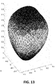
- FIG. 13 shows an iso-intensity surface of scattered light obtained by a simulation.
- FIG. 14 shows a 2D scattering intensity plot of the same simulation, showing the decreasing intensity of scattering from a central area 118 to a peripheral area 119 of the microstructure.
- FIG. 15 shows an exemplary distribution n for the scattering centres, after taking such anisotropy of the microstructures into account.
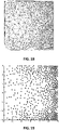
- FIG. 16 and FIG. 17 show respectively a random sampling of microstructures in accordance with this distribution n compensated for the anisotropic scattering of the microstructures, and these randomly sampled microstructure locations adjusted to the nearest position on a grating line.
- the conformity of the grating coupler for providing an approximated point source may be further improved by using meshing tools, e.g. to adjust the spacing between microstructure locations, for example obtained by an initial random sampling as discussed hereinabove, so as to improve a simulated out-coupled field conformity to the target point source distribution in each iteration.
- meshing tools e.g. to adjust the spacing between microstructure locations, for example obtained by an initial random sampling as discussed hereinabove, so as to improve a simulated out-coupled field conformity to the target point source distribution in each iteration.
- FIG. 18 illustrates such mesh
- FIG. 19 and FIG. 20 illustrate the microstructure positioning in two mesh correction iterations.
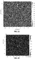
- FIG. 21 to 23 show a simulated field above a light coupler that comprises microstructures as obtained by a procedure described hereinabove.
- FIG. 21 shows the focal spot formed at this distance above the coordinate system origin.
- FIG. 22 shows the focal spot of about 250 nm formed in the focal plane.
- FIG. 23 shows the far field of the light coupled out of the waveguide by the grating coupler.
- a light coupler according to embodiments of the present invention may be particularly suitable for use in an imaging device.
- such imaging device e.g. a lens-free imaging device
- This at least one photonic integrated circuit comprises an integrated waveguide for guiding a light signal and a light coupler according to embodiments of the present invention, optically coupled to the integrated waveguide and adapted for directing the light signal out of a plane of the integrated waveguide as a light beam.
- the imaging device may further comprise at least one imaging detector positioned for imaging an object illuminated by the light beam.
- This object may for example comprise a fluid, e.g. a fluid comprising an immersed biological sample.
- the imaging device may comprise a microfluidic channel for containing the object to be imaged, e.g. to contain a fluid medium to be analysed.
- the imaging device 1 may be a lens-free imaging device, e.g. a device for obtaining a spatial representation of an object by observing a spatial pattern obtained by attenuation, reflection, refraction, diffraction, and/or phase modulation of a light wave incident on the object without requiring an optical lens structure.
- the lens-free imaging device may be a lens-free cell sorting device having a plurality of light couplers and micro-fluidic channels wherein light couplers illuminate objects propagating in the micro-fluidic channels.
- each micro-fluidic channel may comprise a light coupler for illuminating objects.
- the device may for example be adapted for imaging the object under magnification, e.g. for obtaining an image of an object under magnification, such as microscopic imaging.
- This imaging device 1 comprises at least one photonic integrated circuit 2 according to embodiments of the second aspect of the present invention.
- the imaging device 1 may comprise a light source, e.g. an at least partially coherent light source, for providing a light signal 5 to the at least one photonic integrated circuit 2.
- a light source e.g. an at least partially coherent light source
- such light source may comprise a laser or light-emitting diode (LED) to provide at least partially coherent light with a limited bandwidth for coupling to the integrated waveguide on the photonic integrated circuit.
- LED light-emitting diode
- the imaging device 1 further comprises at least one imaging detector 11, such as a CMOS image detector, positioned for imaging an object 12 illuminated by the light beam 9.
- the at least one imaging detector 11 may for example be adapted for imaging the object when the object is positioned downstream of a focal plane with respect to the propagation direction of the light beam, in embodiments where the generated light beam is a focused light beam.
- the imaging device may comprise other parts such as known in the art for performing image acquisition, digitization and/or transmission and/or storage of the image.
- the imaging device may also comprise processing means, e.g. a processor such as an application specific integrated circuit device, adapted for performing image processing operations, such as for example image filtering, image transformation, pattern recognition and/or image compression.
- the object 12 may for example comprise a fluid, e.g. a fluid comprising an immersed biological sample, contained in a microfluidic channel.
- the at least one imaging detector may for example be adapted for acquiring a holographic diffraction image of the object 12 and/or may be adapted for acquiring a fluorescence image of the object 12.
- the device may comprise at least one pinhole 15, positioned in between the photonic integrated circuit 2 and the at least one imaging detector 11 for spatially filtering the light beam 9, e.g. for filtering the light beam before reaching the object.
- the wavefront of a focused light beam may be cleaned up by a pinhole at the focal plane, e.g. the pinhole collimator may implement a low spatial frequency band pass filter.
- the at least one pinhole collimator may thus be positioned in the focal plane for spatially filtering the focused light beam.
- the at least one imaging detector 11 may be adapted for simultaneously imaging a plurality of objects 12, wherein each object of the plurality of objects is positioned such as to allow illumination of each object by a corresponding light beam emitted by a corresponding light coupler according to embodiments of the present invention, e.g. when each object is positioned downstream of the focal plane with respect to the propagation direction of a corresponding focused beam emitted by a corresponding light coupler.
- An imaging device comprising a light coupler according to embodiments may also comprise a reflective surface, wherein the reflective surface and the at least one imaging detector are positioned such that light from the illuminated object and the light beam is reflected by the reflective surface and detected by the at least one imaging detector after reflection.
- the light coupler may be used in a displaying system.
- the displaying system may be a 3D displaying system such as a holographic displaying system.
- Such a system may comprise a plurality of light couplers wherein each light coupler is a focusing light coupler as described above.
- the system may comprise a plurality of waveguides, each waveguide being optically coupled to a light coupler.
- Each light coupler may be designed such that the light signal fed by the waveguide is out-coupled into a focal light spot in free space.
- the plurality of light couplers may be adapted such that the ensemble of focal light spots of different light couplers forms a virtual 3D object in free space, e.g. a holographic object.
- each light coupler may redirect light into a different direction such that each light coupler generates a focal spot at a different location in free space.
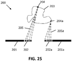
- FIG. 25 illustrates an embodiment of such a displaying system.
- the system comprises a plurality of optical waveguides 201, 201a.
- Each optical waveguide 201, 201a is optically coupled to at least one light coupler 202, 202a, respectively.
- a light signal fed into the optical waveguide 201, 201a is propagated towards the light coupler 202, 202a.
- the light coupler is adapted such that the light signal is coupled out of the optical waveguide as a focused light beam 205, 205a having a focal light spot 204, 204a in free space.
- the plurality of light couplers 202, 202a is adapted such that the ensemble of focal light spots 204, 204a creates a virtual 3D object 203 in the free space, e.g. a holographic object.
Landscapes
- Physics & Mathematics (AREA)
- General Physics & Mathematics (AREA)
- Optics & Photonics (AREA)
- Chemical & Material Sciences (AREA)
- Dispersion Chemistry (AREA)
- Health & Medical Sciences (AREA)
- Life Sciences & Earth Sciences (AREA)
- Analytical Chemistry (AREA)
- Biochemistry (AREA)
- General Health & Medical Sciences (AREA)
- Immunology (AREA)
- Pathology (AREA)
- Engineering & Computer Science (AREA)
- Microelectronics & Electronic Packaging (AREA)
- Computing Systems (AREA)
- Theoretical Computer Science (AREA)
- Optical Integrated Circuits (AREA)
- Optical Couplings Of Light Guides (AREA)
Claims (14)
- Ein Lichtkoppler (8) zum optischen Koppeln an einen integrierten Wellenleiter (4) und zum Auskoppeln eines Lichtsignals (5), das sich in dem integrierten Wellenleiter in einen Freiraum ausbreitet, wobei der Lichtkoppler eine Lichtkopplungsstruktur und eine Vielzahl von Mikrostrukturen (202) umfasst, die auf der Lichtkopplungsstruktur entsprechend einer ungleichmäßigen Zahlendichteverteilung positioniert sind, wobei jede der Mikrostrukturen ein optisches Streuzentrum bildet, wobei die Vielzahl von Mikrostrukturen (202) in Form und Position angeordnet ist, um einen Zerfall des Lichtsignals (5) auszugleichen, wenn es sich in dem Lichtkoppler (8) ausbreitet und eine Leistungsverteilung (201) des Lichtsignals bereitzustellen, wenn es in den Freiraum gekoppelt wird, sodass die Leistungsverteilung (201) einer vorbestimmten Zielleistungsverteilung entspricht,
dadurch gekennzeichnet, dass
die Vielzahl von Mikrostrukturen auf Gitterlinien der Lichtkopplungsstruktur bereitgestellt wird. - Der Lichtkoppler nach Anspruch 1, wobei die ungleichmäßige Zahlendichteverteilung eine diskrete Bemusterungsannäherung einer kontinuierlichen Dichteverteilung ist, die zum Bereitstellen der vorbestimmten Zielleistungsverteilung angepasst ist.
- Ein Lichtkoppler nach einem der vorstehenden Ansprüche, wobei die Vielzahl von Mikrostrukturen (202) in Gestalt und Form angepasst ist, um eine Gauß'sche Leistungsverteilung des Lichtsignals bereitzustellen, wenn es sich im Freiraum ausbreitet.
- Ein Lichtkoppler nach einem der vorstehenden Ansprüche, wobei der Lichtkoppler (8) zum Fokussieren eines ausgekoppelten Lichtsignals in einen Freiraum angepasst ist, wenn ein fokussierter Lichtstrahl in einen Brennpunkt konvergiert.
- Eine 3D-Anzeige, eine Vielzahl von Lichtkopplern nach Anspruch 4 umfassend, wobei die Vielzahl von Lichtkopplern angepasst ist, sodass eine Reihe von Brennpunkten, die durch die Vielzahl von Lichtkopplern erzeugt werden, ein dreidimensionales Bild in einem Freiraum bildet.
- Eine Photonenhalbleiterschaltung (2), einen integrierten Wellenleiter (4) zum Leiten eines Lichtsignals (5) und einen Lichtkoppler (8) nach einem der Ansprüche 1 bis 4 umfassend, wobei der Lichtkoppler (8) optisch mit dem integrierten Wellenleiter (4) gekoppelt ist, und zum Richten des Lichtsignals (5) aus der Ebene des Wellenleiters (4) heraus als einen Lichtstrahl (9) angepasst ist.
- Die Photonenhalbleiterschaltung (2) nach Anspruch 6, wobei der Lichtkoppler einen Teil des integrierten Wellenleiters bildet.
- Die Photonenhalbleiterschaltung (2) nach Anspruch 7, wobei die Vielzahl von Mikrostrukturen mindestens teilweise in dem integrierten Wellenleiter gefertigt ist.
- Die Photonenhalbleiterschaltung (2) nach einem der Ansprüche 7 bis 8, wobei die Vielzahl von Mikrostrukturen Durchgangslöcher in dem integrierten Wellenleiter umfasst.
- Die Photonenhalbleiterschaltung (2) nach einem der Ansprüche 7 bis 9, wobei die Vielzahl von Mikrostrukturen mindestens teilweise auf der Oberseite des integrierten Wellenleiters gefertigt ist.
- Ein Verfahren zum Herstellen eines Lichtkopplers zum optischen Auskoppeln eines Lichtsignals aus einem integrierten Wellenleiter in einen Freiraum, wobei das Verfahren umfasst:- Bestimmen einer ungleichmäßigen Zahlendichteverteilung als eine diskrete Bemusterungsannäherung einer kontinuierlichen Dichteverteilung, die zum Bereitstellen der vorbestimmten Zielleistungsverteilung angepasst ist, und- Herstellen einer Vielzahl von Mikrostrukturen, die optische Streuzentren in und/oder auf einem integrierten Wellenleiter bilden, sodass die Vielzahl von Mikrostrukturen in Gestalt und Position angepasst ist, um einen Zerfall eines Lichtsignals auszugleichen, wenn es sich in dem Lichtkoppler ausbreitet und so, um die vorbestimmte Zielleistungsverteilung des Lichtsignals bereitzustellen, wenn es sich im Freiraum ausbreitet,wobei die Herstellung Positionieren der Mikrostrukturen auf Gitterlinien des Lichtkopplers entsprechend der ungleichmäßigen Zahlendichteverteilung umfasst.
- Verwendung eines Lichtkopplers nach einem der Ansprüche 1 bis 4 in einem Anzeigesystem.
- Verwendung eines Lichtkopplers nach einem der Ansprüche 1 bis 4 in einem 3D-Anzeigesystem.
- Verwendung eines Lichtkopplers nach einem der Ansprüche 1 bis 4 in einem linsenlosen Zellsortiersystem.
Applications Claiming Priority (2)
| Application Number | Priority Date | Filing Date | Title |
|---|---|---|---|
| EP14200427 | 2014-12-29 | ||
| PCT/EP2015/081304 WO2016107851A1 (en) | 2014-12-29 | 2015-12-28 | Light coupler |
Publications (2)
| Publication Number | Publication Date |
|---|---|
| EP3241046A1 EP3241046A1 (de) | 2017-11-08 |
| EP3241046B1 true EP3241046B1 (de) | 2023-01-25 |
Family
ID=52272940
Family Applications (1)
| Application Number | Title | Priority Date | Filing Date |
|---|---|---|---|
| EP15817405.2A Active EP3241046B1 (de) | 2014-12-29 | 2015-12-28 | Lichtkoppler |
Country Status (6)
| Country | Link |
|---|---|
| US (1) | US10564362B2 (de) |
| EP (1) | EP3241046B1 (de) |
| JP (1) | JP2017538970A (de) |
| CN (1) | CN107111057A (de) |
| CA (1) | CA2972327A1 (de) |
| WO (1) | WO2016107851A1 (de) |
Families Citing this family (6)
| Publication number | Priority date | Publication date | Assignee | Title |
|---|---|---|---|---|
| CN105008895B (zh) | 2012-10-15 | 2019-02-15 | 纳诺赛莱克特生物医药股份有限公司 | 颗粒分选的系统、设备和方法 |
| EP3241046B1 (de) * | 2014-12-29 | 2023-01-25 | IMEC vzw | Lichtkoppler |
| WO2016124677A1 (en) * | 2015-02-06 | 2016-08-11 | Imec Vzw | Large area lens-free imaging device |
| DE102016115938A1 (de) * | 2016-08-26 | 2018-03-01 | Carl Zeiss Jena Gmbh | Wellenleiter sowie Vorrichtungen zur Dateneinspiegelung |
| US10244297B1 (en) * | 2018-03-14 | 2019-03-26 | Juniper Networks, Inc. | Reduced crosstalk photonic switch |
| EP4134725B1 (de) * | 2020-04-08 | 2025-02-26 | BGI Shenzhen | Linsenfreies mikroskopisches bildgebungssystem und verfahren sowie system und verfahren zum nachweis biochemischer substanzen |
Family Cites Families (25)
| Publication number | Priority date | Publication date | Assignee | Title |
|---|---|---|---|---|
| US5033812B1 (en) * | 1989-02-17 | 1993-10-12 | Sharp Kabushiki Kaisha | Grating coupler with a tapering waveguide for changing a coupling coefficient |
| US5420947A (en) * | 1994-06-17 | 1995-05-30 | Eastman Kodak Company | Method for achromatically coupling a beam of light into a waveguide |
| US5625729A (en) * | 1994-08-12 | 1997-04-29 | Brown; Thomas G. | Optoelectronic device for coupling between an external optical wave and a local optical wave for optical modulators and detectors |
| JPH0996842A (ja) * | 1995-09-29 | 1997-04-08 | Minolta Co Ltd | 導波路入出力装置 |
| GB9710062D0 (en) * | 1997-05-16 | 1997-07-09 | British Tech Group | Optical devices and methods of fabrication thereof |
| US6760359B2 (en) * | 2000-04-28 | 2004-07-06 | Photodigm, Inc. | Grating-outcoupled surface-emitting lasers with flared gain regions |
| GB0208255D0 (en) * | 2002-04-10 | 2002-05-22 | Imec Inter Uni Micro Electr | Photonic crystal based fiber-to-waveguide coupler for polarisation independent photonic integrated circuits |
| US7184625B2 (en) * | 2003-02-11 | 2007-02-27 | Luxtera, Inc | Optical waveguide grating coupler incorporating reflective optical elements and anti-reflection elements |
| US7245803B2 (en) * | 2003-02-11 | 2007-07-17 | Luxtera, Inc. | Optical waveguide grating coupler |
| US7006732B2 (en) * | 2003-03-21 | 2006-02-28 | Luxtera, Inc. | Polarization splitting grating couplers |
| US7397987B2 (en) * | 2004-05-06 | 2008-07-08 | California Institute Of Technology | Resonantly enhanced grating coupler |
| CN100345013C (zh) * | 2004-11-19 | 2007-10-24 | 东南大学 | 含有光波导内嵌入式倾斜布拉格光栅的装置及光处理方法 |
| KR20070110882A (ko) * | 2005-02-16 | 2007-11-20 | 어플라이드 머티어리얼스, 인코포레이티드 | Ic 칩에 대한 광 결합 |
| FR2893414A1 (fr) * | 2005-11-17 | 2007-05-18 | Philippe Claude Loui Daurenjou | Systeme de differenciation et de denombrement des particules suspendues dans un liquide. |
| WO2009141332A1 (en) * | 2008-05-19 | 2009-11-26 | Interuniversitair Microelektronica Centrum Vzw (Imec) | Integrated photonics device |
| US8494315B2 (en) * | 2009-12-17 | 2013-07-23 | Alcatel Lucent | Photonic integrated circuit having a waveguide-grating coupler |
| EP2618130A1 (de) * | 2012-01-17 | 2013-07-24 | F. Hoffmann-La Roche AG | Vorrichtung zur Verwendung bei der Bindeaffinitätserkennung |
| JP6073470B2 (ja) * | 2012-05-31 | 2017-02-01 | レイア、インコーポレイテッドLeia Inc. | 指向性バックライト |
| GB201209837D0 (en) * | 2012-06-01 | 2012-08-29 | Univ Bristol | Orbital angular momentum |
| KR102152353B1 (ko) * | 2012-10-24 | 2020-09-07 | 시리얼 테크놀로지즈 에스.에이. | 조명 디바이스 |
| CN104508353B (zh) * | 2013-07-30 | 2018-08-31 | 镭亚股份有限公司 | 基于多束衍射光栅的背光照明 |
| WO2016011002A1 (en) * | 2014-07-14 | 2016-01-21 | Biond Photonics Inc. | 3d photonic integration with light coupling elements |
| EP3040750A1 (de) * | 2014-12-29 | 2016-07-06 | IMEC vzw | Vorrichtung und Verfahren zur Durchführung objektfreier Abbildung |
| EP3241046B1 (de) * | 2014-12-29 | 2023-01-25 | IMEC vzw | Lichtkoppler |
| KR102472132B1 (ko) * | 2015-09-18 | 2022-11-29 | 삼성전자주식회사 | 광학 장치 |
-
2015
- 2015-12-28 EP EP15817405.2A patent/EP3241046B1/de active Active
- 2015-12-28 CA CA2972327A patent/CA2972327A1/en not_active Abandoned
- 2015-12-28 US US15/538,926 patent/US10564362B2/en active Active
- 2015-12-28 JP JP2017533460A patent/JP2017538970A/ja active Pending
- 2015-12-28 WO PCT/EP2015/081304 patent/WO2016107851A1/en not_active Ceased
- 2015-12-28 CN CN201580072171.8A patent/CN107111057A/zh active Pending
Also Published As
| Publication number | Publication date |
|---|---|
| US10564362B2 (en) | 2020-02-18 |
| US20170351035A1 (en) | 2017-12-07 |
| JP2017538970A (ja) | 2017-12-28 |
| CN107111057A (zh) | 2017-08-29 |
| CA2972327A1 (en) | 2016-07-07 |
| WO2016107851A1 (en) | 2016-07-07 |
| EP3241046A1 (de) | 2017-11-08 |
Similar Documents
| Publication | Publication Date | Title |
|---|---|---|
| US10267998B2 (en) | Device and method for performing lens-free imaging | |
| EP3241046B1 (de) | Lichtkoppler | |
| US10921236B2 (en) | Integrated lens free imaging device | |
| US11454791B2 (en) | Optical component for generating a periodic light pattern | |
| US10983326B2 (en) | Super-resolution imaging | |
| US11428924B2 (en) | Devices and methods for conveying and controlling light beams for lensless endo-microscopic imagery | |
| JP2007128095A (ja) | 可変近共焦点制御手段を備えた光ファイバ共焦点像形成装置 | |
| JP2018502638A (ja) | レンズなし内視鏡イメージング向けの、光パルスの搬送・制御用装置 | |
| JP2016537659A (ja) | ホログラムを組み込まれた光導波路 | |
| JP2018507386A5 (de) | ||
| CN102818794A (zh) | 生物荧光显微检测仪器 | |
| US9280003B2 (en) | Multimode fiber for spatial scanning | |
| WO2021024420A1 (ja) | 屈折率分布推定システム | |
| CN119596441A (zh) | 一种眼动追踪装置及其制备方法、显示设备 | |
| Brenner | A high-speed version of the wave propagation method applied to micro-optics | |
| Klenk et al. | Modeling Gaussian Beam Propagation in Micro-Droplets with Ray Optics | |
| Darafsheh et al. | Integrated microsphere arrays: light focusing and propagation effects | |
| Momtaj et al. | Toward low-noise on-chip plasmonic three-dimensional biological cell imaging | |
| Darafsheh et al. | Focusing capability of integrated chains of microspheres in the limit of geometrical optics | |
| Xin | Silicon-based Polarization-insensitive Optical Antenna Design and Experimental Characterization of Optical Phased Arrays | |
| Soper | Simulation, fabrication and assembly techniques for passive alignment of silicon photonic integrated circuits | |
| Hosseini et al. | Focusing optical phased array for tissue interrogation with improved side-lobe suppression and simplified beam steering | |
| CN116430569A (zh) | 照明装置、扫描成像方法和全内反射显微成像系统 | |
| Jennings | Dielectric focusing elements for integrated optics | |
| Komiyama | Perturbation analysis of the TE plane wave scattering from the end-face of a waveguide system |
Legal Events
| Date | Code | Title | Description |
|---|---|---|---|
| STAA | Information on the status of an ep patent application or granted ep patent |
Free format text: STATUS: THE INTERNATIONAL PUBLICATION HAS BEEN MADE |
|
| PUAI | Public reference made under article 153(3) epc to a published international application that has entered the european phase |
Free format text: ORIGINAL CODE: 0009012 |
|
| STAA | Information on the status of an ep patent application or granted ep patent |
Free format text: STATUS: REQUEST FOR EXAMINATION WAS MADE |
|
| 17P | Request for examination filed |
Effective date: 20170724 |
|
| AK | Designated contracting states |
Kind code of ref document: A1 Designated state(s): AL AT BE BG CH CY CZ DE DK EE ES FI FR GB GR HR HU IE IS IT LI LT LU LV MC MK MT NL NO PL PT RO RS SE SI SK SM TR |
|
| AX | Request for extension of the european patent |
Extension state: BA ME |
|
| DAV | Request for validation of the european patent (deleted) | ||
| DAX | Request for extension of the european patent (deleted) | ||
| STAA | Information on the status of an ep patent application or granted ep patent |
Free format text: STATUS: EXAMINATION IS IN PROGRESS |
|
| 17Q | First examination report despatched |
Effective date: 20190827 |
|
| RIC1 | Information provided on ipc code assigned before grant |
Ipc: G03H 1/04 20060101ALI20211130BHEP Ipc: G02B 6/24 20060101ALI20211130BHEP Ipc: G02B 6/124 20060101ALI20211130BHEP Ipc: G01N 15/14 20060101ALI20211130BHEP Ipc: F21V 8/00 20060101ALI20211130BHEP Ipc: G02B 27/09 20060101AFI20211130BHEP |
|
| GRAP | Despatch of communication of intention to grant a patent |
Free format text: ORIGINAL CODE: EPIDOSNIGR1 |
|
| STAA | Information on the status of an ep patent application or granted ep patent |
Free format text: STATUS: GRANT OF PATENT IS INTENDED |
|
| INTG | Intention to grant announced |
Effective date: 20220121 |
|
| GRAJ | Information related to disapproval of communication of intention to grant by the applicant or resumption of examination proceedings by the epo deleted |
Free format text: ORIGINAL CODE: EPIDOSDIGR1 |
|
| STAA | Information on the status of an ep patent application or granted ep patent |
Free format text: STATUS: EXAMINATION IS IN PROGRESS |
|
| REG | Reference to a national code |
Ref country code: DE Ref legal event code: R079 Ref document number: 602015082403 Country of ref document: DE Free format text: PREVIOUS MAIN CLASS: G02B0006240000 Ipc: G02B0030560000 |
|
| INTC | Intention to grant announced (deleted) | ||
| RIC1 | Information provided on ipc code assigned before grant |
Ipc: G02B 30/56 20200101AFI20220704BHEP |
|
| INTG | Intention to grant announced |
Effective date: 20220812 |
|
| INTG | Intention to grant announced |
Effective date: 20220812 |
|
| GRAS | Grant fee paid |
Free format text: ORIGINAL CODE: EPIDOSNIGR3 |
|
| STAA | Information on the status of an ep patent application or granted ep patent |
Free format text: STATUS: GRANT OF PATENT IS INTENDED |
|
| GRAA | (expected) grant |
Free format text: ORIGINAL CODE: 0009210 |
|
| STAA | Information on the status of an ep patent application or granted ep patent |
Free format text: STATUS: THE PATENT HAS BEEN GRANTED |
|
| AK | Designated contracting states |
Kind code of ref document: B1 Designated state(s): AL AT BE BG CH CY CZ DE DK EE ES FI FR GB GR HR HU IE IS IT LI LT LU LV MC MK MT NL NO PL PT RO RS SE SI SK SM TR |
|
| REG | Reference to a national code |
Ref country code: GB Ref legal event code: FG4D |
|
| REG | Reference to a national code |
Ref country code: CH Ref legal event code: EP |
|
| REG | Reference to a national code |
Ref country code: AT Ref legal event code: REF Ref document number: 1546283 Country of ref document: AT Kind code of ref document: T Effective date: 20230215 Ref country code: IE Ref legal event code: FG4D |
|
| REG | Reference to a national code |
Ref country code: DE Ref legal event code: R096 Ref document number: 602015082403 Country of ref document: DE |
|
| REG | Reference to a national code |
Ref country code: LT Ref legal event code: MG9D |
|
| REG | Reference to a national code |
Ref country code: NL Ref legal event code: MP Effective date: 20230125 |
|
| REG | Reference to a national code |
Ref country code: AT Ref legal event code: MK05 Ref document number: 1546283 Country of ref document: AT Kind code of ref document: T Effective date: 20230125 |
|
| P01 | Opt-out of the competence of the unified patent court (upc) registered |
Effective date: 20230513 |
|
| PG25 | Lapsed in a contracting state [announced via postgrant information from national office to epo] |
Ref country code: NL Free format text: LAPSE BECAUSE OF FAILURE TO SUBMIT A TRANSLATION OF THE DESCRIPTION OR TO PAY THE FEE WITHIN THE PRESCRIBED TIME-LIMIT Effective date: 20230125 |
|
| PG25 | Lapsed in a contracting state [announced via postgrant information from national office to epo] |
Ref country code: RS Free format text: LAPSE BECAUSE OF FAILURE TO SUBMIT A TRANSLATION OF THE DESCRIPTION OR TO PAY THE FEE WITHIN THE PRESCRIBED TIME-LIMIT Effective date: 20230125 Ref country code: PT Free format text: LAPSE BECAUSE OF FAILURE TO SUBMIT A TRANSLATION OF THE DESCRIPTION OR TO PAY THE FEE WITHIN THE PRESCRIBED TIME-LIMIT Effective date: 20230525 Ref country code: NO Free format text: LAPSE BECAUSE OF FAILURE TO SUBMIT A TRANSLATION OF THE DESCRIPTION OR TO PAY THE FEE WITHIN THE PRESCRIBED TIME-LIMIT Effective date: 20230425 Ref country code: LV Free format text: LAPSE BECAUSE OF FAILURE TO SUBMIT A TRANSLATION OF THE DESCRIPTION OR TO PAY THE FEE WITHIN THE PRESCRIBED TIME-LIMIT Effective date: 20230125 Ref country code: LT Free format text: LAPSE BECAUSE OF FAILURE TO SUBMIT A TRANSLATION OF THE DESCRIPTION OR TO PAY THE FEE WITHIN THE PRESCRIBED TIME-LIMIT Effective date: 20230125 Ref country code: HR Free format text: LAPSE BECAUSE OF FAILURE TO SUBMIT A TRANSLATION OF THE DESCRIPTION OR TO PAY THE FEE WITHIN THE PRESCRIBED TIME-LIMIT Effective date: 20230125 Ref country code: ES Free format text: LAPSE BECAUSE OF FAILURE TO SUBMIT A TRANSLATION OF THE DESCRIPTION OR TO PAY THE FEE WITHIN THE PRESCRIBED TIME-LIMIT Effective date: 20230125 Ref country code: AT Free format text: LAPSE BECAUSE OF FAILURE TO SUBMIT A TRANSLATION OF THE DESCRIPTION OR TO PAY THE FEE WITHIN THE PRESCRIBED TIME-LIMIT Effective date: 20230125 |
|
| PG25 | Lapsed in a contracting state [announced via postgrant information from national office to epo] |
Ref country code: SE Free format text: LAPSE BECAUSE OF FAILURE TO SUBMIT A TRANSLATION OF THE DESCRIPTION OR TO PAY THE FEE WITHIN THE PRESCRIBED TIME-LIMIT Effective date: 20230125 Ref country code: PL Free format text: LAPSE BECAUSE OF FAILURE TO SUBMIT A TRANSLATION OF THE DESCRIPTION OR TO PAY THE FEE WITHIN THE PRESCRIBED TIME-LIMIT Effective date: 20230125 Ref country code: IS Free format text: LAPSE BECAUSE OF FAILURE TO SUBMIT A TRANSLATION OF THE DESCRIPTION OR TO PAY THE FEE WITHIN THE PRESCRIBED TIME-LIMIT Effective date: 20230525 Ref country code: GR Free format text: LAPSE BECAUSE OF FAILURE TO SUBMIT A TRANSLATION OF THE DESCRIPTION OR TO PAY THE FEE WITHIN THE PRESCRIBED TIME-LIMIT Effective date: 20230426 Ref country code: FI Free format text: LAPSE BECAUSE OF FAILURE TO SUBMIT A TRANSLATION OF THE DESCRIPTION OR TO PAY THE FEE WITHIN THE PRESCRIBED TIME-LIMIT Effective date: 20230125 |
|
| REG | Reference to a national code |
Ref country code: DE Ref legal event code: R097 Ref document number: 602015082403 Country of ref document: DE |
|
| PG25 | Lapsed in a contracting state [announced via postgrant information from national office to epo] |
Ref country code: SM Free format text: LAPSE BECAUSE OF FAILURE TO SUBMIT A TRANSLATION OF THE DESCRIPTION OR TO PAY THE FEE WITHIN THE PRESCRIBED TIME-LIMIT Effective date: 20230125 Ref country code: RO Free format text: LAPSE BECAUSE OF FAILURE TO SUBMIT A TRANSLATION OF THE DESCRIPTION OR TO PAY THE FEE WITHIN THE PRESCRIBED TIME-LIMIT Effective date: 20230125 Ref country code: EE Free format text: LAPSE BECAUSE OF FAILURE TO SUBMIT A TRANSLATION OF THE DESCRIPTION OR TO PAY THE FEE WITHIN THE PRESCRIBED TIME-LIMIT Effective date: 20230125 Ref country code: DK Free format text: LAPSE BECAUSE OF FAILURE TO SUBMIT A TRANSLATION OF THE DESCRIPTION OR TO PAY THE FEE WITHIN THE PRESCRIBED TIME-LIMIT Effective date: 20230125 Ref country code: CZ Free format text: LAPSE BECAUSE OF FAILURE TO SUBMIT A TRANSLATION OF THE DESCRIPTION OR TO PAY THE FEE WITHIN THE PRESCRIBED TIME-LIMIT Effective date: 20230125 |
|
| PG25 | Lapsed in a contracting state [announced via postgrant information from national office to epo] |
Ref country code: SK Free format text: LAPSE BECAUSE OF FAILURE TO SUBMIT A TRANSLATION OF THE DESCRIPTION OR TO PAY THE FEE WITHIN THE PRESCRIBED TIME-LIMIT Effective date: 20230125 |
|
| PLBE | No opposition filed within time limit |
Free format text: ORIGINAL CODE: 0009261 |
|
| STAA | Information on the status of an ep patent application or granted ep patent |
Free format text: STATUS: NO OPPOSITION FILED WITHIN TIME LIMIT |
|
| 26N | No opposition filed |
Effective date: 20231026 |
|
| PG25 | Lapsed in a contracting state [announced via postgrant information from national office to epo] |
Ref country code: SI Free format text: LAPSE BECAUSE OF FAILURE TO SUBMIT A TRANSLATION OF THE DESCRIPTION OR TO PAY THE FEE WITHIN THE PRESCRIBED TIME-LIMIT Effective date: 20230125 |
|
| PG25 | Lapsed in a contracting state [announced via postgrant information from national office to epo] |
Ref country code: IT Free format text: LAPSE BECAUSE OF FAILURE TO SUBMIT A TRANSLATION OF THE DESCRIPTION OR TO PAY THE FEE WITHIN THE PRESCRIBED TIME-LIMIT Effective date: 20230125 |
|
| REG | Reference to a national code |
Ref country code: CH Ref legal event code: PL |
|
| PG25 | Lapsed in a contracting state [announced via postgrant information from national office to epo] |
Ref country code: LU Free format text: LAPSE BECAUSE OF NON-PAYMENT OF DUE FEES Effective date: 20231228 |
|
| PG25 | Lapsed in a contracting state [announced via postgrant information from national office to epo] |
Ref country code: MC Free format text: LAPSE BECAUSE OF FAILURE TO SUBMIT A TRANSLATION OF THE DESCRIPTION OR TO PAY THE FEE WITHIN THE PRESCRIBED TIME-LIMIT Effective date: 20230125 |
|
| GBPC | Gb: european patent ceased through non-payment of renewal fee |
Effective date: 20231228 |
|
| REG | Reference to a national code |
Ref country code: BE Ref legal event code: MM Effective date: 20231231 |
|
| PG25 | Lapsed in a contracting state [announced via postgrant information from national office to epo] |
Ref country code: MC Free format text: LAPSE BECAUSE OF FAILURE TO SUBMIT A TRANSLATION OF THE DESCRIPTION OR TO PAY THE FEE WITHIN THE PRESCRIBED TIME-LIMIT Effective date: 20230125 Ref country code: LU Free format text: LAPSE BECAUSE OF NON-PAYMENT OF DUE FEES Effective date: 20231228 |
|
| REG | Reference to a national code |
Ref country code: IE Ref legal event code: MM4A |
|
| PG25 | Lapsed in a contracting state [announced via postgrant information from national office to epo] |
Ref country code: IE Free format text: LAPSE BECAUSE OF NON-PAYMENT OF DUE FEES Effective date: 20231228 |
|
| PG25 | Lapsed in a contracting state [announced via postgrant information from national office to epo] |
Ref country code: GB Free format text: LAPSE BECAUSE OF NON-PAYMENT OF DUE FEES Effective date: 20231228 |
|
| PG25 | Lapsed in a contracting state [announced via postgrant information from national office to epo] |
Ref country code: BE Free format text: LAPSE BECAUSE OF NON-PAYMENT OF DUE FEES Effective date: 20231231 |
|
| PG25 | Lapsed in a contracting state [announced via postgrant information from national office to epo] |
Ref country code: CH Free format text: LAPSE BECAUSE OF NON-PAYMENT OF DUE FEES Effective date: 20231231 |
|
| PG25 | Lapsed in a contracting state [announced via postgrant information from national office to epo] |
Ref country code: IE Free format text: LAPSE BECAUSE OF NON-PAYMENT OF DUE FEES Effective date: 20231228 Ref country code: GB Free format text: LAPSE BECAUSE OF NON-PAYMENT OF DUE FEES Effective date: 20231228 Ref country code: CH Free format text: LAPSE BECAUSE OF NON-PAYMENT OF DUE FEES Effective date: 20231231 Ref country code: BE Free format text: LAPSE BECAUSE OF NON-PAYMENT OF DUE FEES Effective date: 20231231 |
|
| PG25 | Lapsed in a contracting state [announced via postgrant information from national office to epo] |
Ref country code: BG Free format text: LAPSE BECAUSE OF FAILURE TO SUBMIT A TRANSLATION OF THE DESCRIPTION OR TO PAY THE FEE WITHIN THE PRESCRIBED TIME-LIMIT Effective date: 20230125 |
|
| PG25 | Lapsed in a contracting state [announced via postgrant information from national office to epo] |
Ref country code: BG Free format text: LAPSE BECAUSE OF FAILURE TO SUBMIT A TRANSLATION OF THE DESCRIPTION OR TO PAY THE FEE WITHIN THE PRESCRIBED TIME-LIMIT Effective date: 20230125 |
|
| PG25 | Lapsed in a contracting state [announced via postgrant information from national office to epo] |
Ref country code: CY Free format text: LAPSE BECAUSE OF FAILURE TO SUBMIT A TRANSLATION OF THE DESCRIPTION OR TO PAY THE FEE WITHIN THE PRESCRIBED TIME-LIMIT; INVALID AB INITIO Effective date: 20151228 |
|
| PG25 | Lapsed in a contracting state [announced via postgrant information from national office to epo] |
Ref country code: HU Free format text: LAPSE BECAUSE OF FAILURE TO SUBMIT A TRANSLATION OF THE DESCRIPTION OR TO PAY THE FEE WITHIN THE PRESCRIBED TIME-LIMIT; INVALID AB INITIO Effective date: 20151228 |
|
| PG25 | Lapsed in a contracting state [announced via postgrant information from national office to epo] |
Ref country code: TR Free format text: LAPSE BECAUSE OF FAILURE TO SUBMIT A TRANSLATION OF THE DESCRIPTION OR TO PAY THE FEE WITHIN THE PRESCRIBED TIME-LIMIT Effective date: 20230125 |
|
| PGFP | Annual fee paid to national office [announced via postgrant information from national office to epo] |
Ref country code: DE Payment date: 20251126 Year of fee payment: 11 |
|
| PGFP | Annual fee paid to national office [announced via postgrant information from national office to epo] |
Ref country code: FR Payment date: 20251120 Year of fee payment: 11 |