EP3241236B1 - Structure de pixels, son procédé d'affichage et afficheur - Google Patents
Structure de pixels, son procédé d'affichage et afficheur Download PDFInfo
- Publication number
- EP3241236B1 EP3241236B1 EP15851646.8A EP15851646A EP3241236B1 EP 3241236 B1 EP3241236 B1 EP 3241236B1 EP 15851646 A EP15851646 A EP 15851646A EP 3241236 B1 EP3241236 B1 EP 3241236B1
- Authority
- EP
- European Patent Office
- Prior art keywords
- sub
- pixel
- pixels
- adjacent
- axis
- Prior art date
- Legal status (The legal status is an assumption and is not a legal conclusion. Google has not performed a legal analysis and makes no representation as to the accuracy of the status listed.)
- Active
Links
Images


Classifications
-
- G—PHYSICS
- G09—EDUCATION; CRYPTOGRAPHY; DISPLAY; ADVERTISING; SEALS
- G09G—ARRANGEMENTS OR CIRCUITS FOR CONTROL OF INDICATING DEVICES USING STATIC MEANS TO PRESENT VARIABLE INFORMATION
- G09G3/00—Control arrangements or circuits, of interest only in connection with visual indicators other than cathode-ray tubes
- G09G3/20—Control arrangements or circuits, of interest only in connection with visual indicators other than cathode-ray tubes for presentation of an assembly of a number of characters, e.g. a page, by composing the assembly by combination of individual elements arranged in a matrix no fixed position being assigned to or needed to be assigned to the individual characters or partial characters
- G09G3/2003—Display of colours
-
- H—ELECTRICITY
- H10—SEMICONDUCTOR DEVICES; ELECTRIC SOLID-STATE DEVICES NOT OTHERWISE PROVIDED FOR
- H10K—ORGANIC ELECTRIC SOLID-STATE DEVICES
- H10K59/00—Integrated devices, or assemblies of multiple devices, comprising at least one organic light-emitting element covered by group H10K50/00
- H10K59/30—Devices specially adapted for multicolour light emission
- H10K59/35—Devices specially adapted for multicolour light emission comprising red-green-blue [RGB] subpixels
- H10K59/353—Devices specially adapted for multicolour light emission comprising red-green-blue [RGB] subpixels characterised by the geometrical arrangement of the RGB subpixels
-
- G—PHYSICS
- G09—EDUCATION; CRYPTOGRAPHY; DISPLAY; ADVERTISING; SEALS
- G09G—ARRANGEMENTS OR CIRCUITS FOR CONTROL OF INDICATING DEVICES USING STATIC MEANS TO PRESENT VARIABLE INFORMATION
- G09G3/00—Control arrangements or circuits, of interest only in connection with visual indicators other than cathode-ray tubes
- G09G3/20—Control arrangements or circuits, of interest only in connection with visual indicators other than cathode-ray tubes for presentation of an assembly of a number of characters, e.g. a page, by composing the assembly by combination of individual elements arranged in a matrix no fixed position being assigned to or needed to be assigned to the individual characters or partial characters
- G09G3/2007—Display of intermediate tones
- G09G3/2074—Display of intermediate tones using sub-pixels
-
- G—PHYSICS
- G09—EDUCATION; CRYPTOGRAPHY; DISPLAY; ADVERTISING; SEALS
- G09G—ARRANGEMENTS OR CIRCUITS FOR CONTROL OF INDICATING DEVICES USING STATIC MEANS TO PRESENT VARIABLE INFORMATION
- G09G3/00—Control arrangements or circuits, of interest only in connection with visual indicators other than cathode-ray tubes
- G09G3/20—Control arrangements or circuits, of interest only in connection with visual indicators other than cathode-ray tubes for presentation of an assembly of a number of characters, e.g. a page, by composing the assembly by combination of individual elements arranged in a matrix no fixed position being assigned to or needed to be assigned to the individual characters or partial characters
- G09G3/22—Control arrangements or circuits, of interest only in connection with visual indicators other than cathode-ray tubes for presentation of an assembly of a number of characters, e.g. a page, by composing the assembly by combination of individual elements arranged in a matrix no fixed position being assigned to or needed to be assigned to the individual characters or partial characters using controlled light sources
- G09G3/30—Control arrangements or circuits, of interest only in connection with visual indicators other than cathode-ray tubes for presentation of an assembly of a number of characters, e.g. a page, by composing the assembly by combination of individual elements arranged in a matrix no fixed position being assigned to or needed to be assigned to the individual characters or partial characters using controlled light sources using electroluminescent panels
- G09G3/32—Control arrangements or circuits, of interest only in connection with visual indicators other than cathode-ray tubes for presentation of an assembly of a number of characters, e.g. a page, by composing the assembly by combination of individual elements arranged in a matrix no fixed position being assigned to or needed to be assigned to the individual characters or partial characters using controlled light sources using electroluminescent panels semiconductive, e.g. using light-emitting diodes [LED]
- G09G3/3208—Control arrangements or circuits, of interest only in connection with visual indicators other than cathode-ray tubes for presentation of an assembly of a number of characters, e.g. a page, by composing the assembly by combination of individual elements arranged in a matrix no fixed position being assigned to or needed to be assigned to the individual characters or partial characters using controlled light sources using electroluminescent panels semiconductive, e.g. using light-emitting diodes [LED] organic, e.g. using organic light-emitting diodes [OLED]
- G09G3/3225—Control arrangements or circuits, of interest only in connection with visual indicators other than cathode-ray tubes for presentation of an assembly of a number of characters, e.g. a page, by composing the assembly by combination of individual elements arranged in a matrix no fixed position being assigned to or needed to be assigned to the individual characters or partial characters using controlled light sources using electroluminescent panels semiconductive, e.g. using light-emitting diodes [LED] organic, e.g. using organic light-emitting diodes [OLED] using an active matrix
-
- G—PHYSICS
- G09—EDUCATION; CRYPTOGRAPHY; DISPLAY; ADVERTISING; SEALS
- G09G—ARRANGEMENTS OR CIRCUITS FOR CONTROL OF INDICATING DEVICES USING STATIC MEANS TO PRESENT VARIABLE INFORMATION
- G09G3/00—Control arrangements or circuits, of interest only in connection with visual indicators other than cathode-ray tubes
- G09G3/20—Control arrangements or circuits, of interest only in connection with visual indicators other than cathode-ray tubes for presentation of an assembly of a number of characters, e.g. a page, by composing the assembly by combination of individual elements arranged in a matrix no fixed position being assigned to or needed to be assigned to the individual characters or partial characters
- G09G3/34—Control arrangements or circuits, of interest only in connection with visual indicators other than cathode-ray tubes for presentation of an assembly of a number of characters, e.g. a page, by composing the assembly by combination of individual elements arranged in a matrix no fixed position being assigned to or needed to be assigned to the individual characters or partial characters by control of light from an independent source
- G09G3/36—Control arrangements or circuits, of interest only in connection with visual indicators other than cathode-ray tubes for presentation of an assembly of a number of characters, e.g. a page, by composing the assembly by combination of individual elements arranged in a matrix no fixed position being assigned to or needed to be assigned to the individual characters or partial characters by control of light from an independent source using liquid crystals
- G09G3/3607—Control arrangements or circuits, of interest only in connection with visual indicators other than cathode-ray tubes for presentation of an assembly of a number of characters, e.g. a page, by composing the assembly by combination of individual elements arranged in a matrix no fixed position being assigned to or needed to be assigned to the individual characters or partial characters by control of light from an independent source using liquid crystals for displaying colours or for displaying grey scales with a specific pixel layout, e.g. using sub-pixels
-
- H—ELECTRICITY
- H10—SEMICONDUCTOR DEVICES; ELECTRIC SOLID-STATE DEVICES NOT OTHERWISE PROVIDED FOR
- H10K—ORGANIC ELECTRIC SOLID-STATE DEVICES
- H10K59/00—Integrated devices, or assemblies of multiple devices, comprising at least one organic light-emitting element covered by group H10K50/00
- H10K59/10—OLED displays
- H10K59/12—Active-matrix OLED [AMOLED] displays
- H10K59/131—Interconnections, e.g. wiring lines or terminals
-
- H—ELECTRICITY
- H10—SEMICONDUCTOR DEVICES; ELECTRIC SOLID-STATE DEVICES NOT OTHERWISE PROVIDED FOR
- H10K—ORGANIC ELECTRIC SOLID-STATE DEVICES
- H10K59/00—Integrated devices, or assemblies of multiple devices, comprising at least one organic light-emitting element covered by group H10K50/00
- H10K59/30—Devices specially adapted for multicolour light emission
- H10K59/35—Devices specially adapted for multicolour light emission comprising red-green-blue [RGB] subpixels
- H10K59/352—Devices specially adapted for multicolour light emission comprising red-green-blue [RGB] subpixels the areas of the RGB subpixels being different
-
- H—ELECTRICITY
- H10—SEMICONDUCTOR DEVICES; ELECTRIC SOLID-STATE DEVICES NOT OTHERWISE PROVIDED FOR
- H10K—ORGANIC ELECTRIC SOLID-STATE DEVICES
- H10K71/00—Manufacture or treatment specially adapted for the organic devices covered by this subclass
- H10K71/10—Deposition of organic active material
- H10K71/16—Deposition of organic active material using physical vapour deposition [PVD], e.g. vacuum deposition or sputtering
- H10K71/164—Deposition of organic active material using physical vapour deposition [PVD], e.g. vacuum deposition or sputtering using vacuum deposition
-
- H—ELECTRICITY
- H10—SEMICONDUCTOR DEVICES; ELECTRIC SOLID-STATE DEVICES NOT OTHERWISE PROVIDED FOR
- H10K—ORGANIC ELECTRIC SOLID-STATE DEVICES
- H10K71/00—Manufacture or treatment specially adapted for the organic devices covered by this subclass
- H10K71/10—Deposition of organic active material
- H10K71/16—Deposition of organic active material using physical vapour deposition [PVD], e.g. vacuum deposition or sputtering
- H10K71/166—Deposition of organic active material using physical vapour deposition [PVD], e.g. vacuum deposition or sputtering using selective deposition, e.g. using a mask
-
- G—PHYSICS
- G02—OPTICS
- G02F—OPTICAL DEVICES OR ARRANGEMENTS FOR THE CONTROL OF LIGHT BY MODIFICATION OF THE OPTICAL PROPERTIES OF THE MEDIA OF THE ELEMENTS INVOLVED THEREIN; NON-LINEAR OPTICS; FREQUENCY-CHANGING OF LIGHT; OPTICAL LOGIC ELEMENTS; OPTICAL ANALOGUE/DIGITAL CONVERTERS
- G02F2201/00—Constructional arrangements not provided for in groups G02F1/00 - G02F7/00
- G02F2201/52—RGB geometrical arrangements
-
- G—PHYSICS
- G09—EDUCATION; CRYPTOGRAPHY; DISPLAY; ADVERTISING; SEALS
- G09G—ARRANGEMENTS OR CIRCUITS FOR CONTROL OF INDICATING DEVICES USING STATIC MEANS TO PRESENT VARIABLE INFORMATION
- G09G2300/00—Aspects of the constitution of display devices
- G09G2300/04—Structural and physical details of display devices
- G09G2300/0439—Pixel structures
- G09G2300/0452—Details of colour pixel setup, e.g. pixel composed of a red, a blue and two green components
-
- G—PHYSICS
- G09—EDUCATION; CRYPTOGRAPHY; DISPLAY; ADVERTISING; SEALS
- G09G—ARRANGEMENTS OR CIRCUITS FOR CONTROL OF INDICATING DEVICES USING STATIC MEANS TO PRESENT VARIABLE INFORMATION
- G09G2300/00—Aspects of the constitution of display devices
- G09G2300/04—Structural and physical details of display devices
- G09G2300/0439—Pixel structures
- G09G2300/0465—Improved aperture ratio, e.g. by size reduction of the pixel circuit, e.g. for improving the pixel density or the maximum displayable luminance or brightness
-
- G—PHYSICS
- G09—EDUCATION; CRYPTOGRAPHY; DISPLAY; ADVERTISING; SEALS
- G09G—ARRANGEMENTS OR CIRCUITS FOR CONTROL OF INDICATING DEVICES USING STATIC MEANS TO PRESENT VARIABLE INFORMATION
- G09G2320/00—Control of display operating conditions
- G09G2320/02—Improving the quality of display appearance
- G09G2320/0233—Improving the luminance or brightness uniformity across the screen
-
- G—PHYSICS
- G09—EDUCATION; CRYPTOGRAPHY; DISPLAY; ADVERTISING; SEALS
- G09G—ARRANGEMENTS OR CIRCUITS FOR CONTROL OF INDICATING DEVICES USING STATIC MEANS TO PRESENT VARIABLE INFORMATION
- G09G2320/00—Control of display operating conditions
- G09G2320/04—Maintaining the quality of display appearance
- G09G2320/043—Preventing or counteracting the effects of ageing
-
- G—PHYSICS
- G09—EDUCATION; CRYPTOGRAPHY; DISPLAY; ADVERTISING; SEALS
- G09G—ARRANGEMENTS OR CIRCUITS FOR CONTROL OF INDICATING DEVICES USING STATIC MEANS TO PRESENT VARIABLE INFORMATION
- G09G2360/00—Aspects of the architecture of display systems
- G09G2360/14—Detecting light within display terminals, e.g. using a single or a plurality of photosensors
- G09G2360/145—Detecting light within display terminals, e.g. using a single or a plurality of photosensors the light originating from the display screen
- G09G2360/147—Detecting light within display terminals, e.g. using a single or a plurality of photosensors the light originating from the display screen the originated light output being determined for each pixel
Definitions
- the present invention generally relates to the display technologies and, more particularly, relates to a pixel structure and related displaying method thereof, and a display apparatus containing the same.
- Flat display apparatuses generally include LCD (Liquid Crystal Display) apparatuses and OLED (Organic Light-Emitting Diode) display apparatuses.
- LCD Liquid Crystal Display
- OLED Organic Light-Emitting Diode
- an OLED display has advantages such as being self-luminous, having faster response, and providing a wider viewing angle.
- OLED displays are often suitable for flexible displays, transparent displays, three-dimensional displays, and many other display applications.
- an FMM Feine Metal Mask
- AMOLED Active Matrix Organic Light-Emitting Diode
- the FMM is often used in a deposition process for forming the organic light-emitting layer.
- the opening size of the FMM is often subjected to a restriction of minimum opening size.
- a distance between sub-pixels for displaying a same color may be subjected to certain restrictions such that the distance between two sub-pixels for displaying one color may be different from the distance between two sub-pixels for displaying another color.
- the manufacturing of AMOLED display panels may be inevitably limited by the opening size of the FMM and precision of the deposition process. It might be difficult to obtain high resolution. Particularly, it may difficult to obtain the aperture ratio of the sub-pixels required for providing high resolutions.
- the aperture ratio of the display panel may further affect the product lifespan, display brightness, etc.
- a U.S. patent application, US6714206 provides a method and system for establishing intensity levels for sub-pixels of a display device with overlapping logical pixels.
- the dithering system combines frame rate control techniques with contributions from overlapping pixels to establish the intensity level of each sub-pixel.
- the dithering system initially provides an assignment of frame numbers to each sub-pixel.
- the dithering system then receives a logical pixel color that includes an intensity value for each component color (e.g., red, green, and blue) for each logical pixel.
- the dithering system maps each component intensity value of each logical pixel to an intensity value with a low depth plus a remainder.
- the dithering system generates a sub-pixel intensity value for each sub-pixel of each logical pixel using frame rate control to adjust the intensity value of each sub-pixel based on the remainder and current frame number.
- the dithering system then calculates the intensity value for a sub-pixel by combining all the generated sub-pixel intensity values for that sub-pixel..
- the present invention addresses the above problems in the prior art.
- the present disclosure provides a pixel structure, a method for displaying the pixel structure, and a display apparatus containing the pixel structure.
- the pixel structure can realize high resolution and improve the aperture ratio of the sub-pixels to obtain desirable display brightness.
- the present disclosure thus simplifies the manufacturing process and extends/improves the product service time of the display panels.
- the pixel structure includes first sub-pixels, second sub-pixels, and third sub-pixels. Two adjacent third sub-pixels facing each other form a third sub-pixel group.
- the second sub-pixels are arranged in a row along a first axis to form second-sub-pixel rows, the first sub-pixels and the third sub-pixel groups are arranged in an alternating configuration along the direction of the first axis parallel to the second-sub-pixel rows, and the second-sub-pixel rows and rows formed by the first sub-pixels and the third sub-pixel groups are arranged in an alternating configuration.
- the second sub-pixels are arranged along a direction of a second axis to form second-sub-pixel columns, the first sub-pixels and the third sub-pixel groups are arranged in an alternating configuration along the direction of the second axis parallel to the second-sub-pixel columns, the second-sub-pixel columns and columns formed by the first sub-pixels and the third sub-pixel groups are arranged in an alternating configuration.
- Geometric center of each second sub-pixel is positioned on a perpendicular bisection of a line connecting centers of any two of third sub-pixel groups and first sub-pixels adjacent to the second sub-pixel.
- the second sub-pixel, an adjacent third sub-pixel group in an adjacent row, and an adjacent first sub-pixel in the adjacent row form a pixel unit, consecutive pixel units form pixel unit rows aligned along the direction of the row axis, and except for a first or a last pixel unit in an odd and/or even pixel unit row (e.g., at the edge of a pixel unit row), each pixel unit shares the first sub-pixel with an adjacent pixel unit in a same pixel unit row.
- the second sub-pixel, an adjacent third sub-pixel group in an adjacent column, and an adjacent first sub-pixel in the adjacent column form a pixel unit, consecutive pixel units form pixel unit columns aligned along the direction of the column axis; and except for a first or a last pixel unit in an odd or even pixel unit column, each pixel unit shares the first sub-pixel with an adjacent pixel unit in a same pixel unit column.
- Geometric centers of the first sub-pixels in consecutive rows and consecutive columns are aligned to form lines along a diagonal direction different from the directions of the row axis and the direction of the column axis.
- Geometric centers of the third sub-pixel groups in consecutive rows and consecutive columns are aligned to form lines along the diagonal direction to be parallel to lines formed by the geometric centers of the first sub-pixels such that the lines formed by the geometric centers of the first sub-pixels and lines formed by the geometric centers of third sub-pixel groups are arranged in an alternating configuration, wherein the diagonal direction is 45 degrees clockwise or counter clockwise with the direction of the row axis or the direction of the column axis.
- Each second sub-pixel is aligned between two adjacent first sub-pixels and two adjacent third sub-pixel groups, wherein the two adjacent first sub-pixels are aligned in the diagonal direction and the two adjacent third sub-pixel groups are aligned in the diagonal direction.
- a geometric center of each second sub-pixel is arranged at an intersection of a perpendicular bisector of a line connecting geometric centers of adjacent first sub-pixel and third sub-pixel group in an adjacent row and a perpendicular bisector of a line connecting geometric centers of adjacent first sub-pixel and third sub-pixel group in an adjacent column.
- each of the two third sub-pixels in the third sub-pixel group is a mirror image of the other along the direction of the row axis or along the direction of the column axis
- each third sub-pixel group are arranged between two first sub-pixels along the direction of the row axis or along the direction of the column axis
- two adjacent third sub-pixels are arranged on both sides of the first sub-pixel
- each of the two adjacent third sub-pixels has a shortest distance to the first sub-pixel along the direction of the row axis or along the direction of the column axis such that the two adjacent third sub-pixels have a mirror symmetry or a centrosymmetry about a geometric center of the first sub-pixel.
- each third sub-pixel group is arranged between two adjacent second sub-pixels along a diagonal direction such that each second sub-pixel is arranged between two adjacent third sub-pixel groups along the diagonal direction, and the two adjacent third sub-pixel groups have a mirror symmetry or a centrosymmetry about a geometric center of the second sub-pixel.
- a shape of the first sub-pixel, a shape of the third sub-pixel group, and a shape of the second sub-pixel each has a symmetry axis; and a symmetry axis of the shape of the first sub-pixel extends along a direction parallel to one of the row axis, column axis, and diagonal axis, a symmetry axis of the shape of the third sub-pixel group extends along a direction parallel to one of the row axis, column axis, and diagonal axis, and a symmetry axis of the shape of the second sub-pixel extends along a direction parallel to one of the row axis, column axis, and diagonal axis.
- the lines formed by the geometric centers of the first sub-pixels are arranged along a direction of 45 degrees or 135 degrees with the row axis
- the lines formed by the geometric centers of the third sub-pixel groups are arranged along a direction of 45 degrees or 135 degrees with the row axis
- the lines formed by the geometric centers of the second sub-pixels are arranged along a direction of 45 degrees or 135 degrees with the row axis.
- each of the shape of the first sub-pixel, the shape of the third sub-pixel, the shape of the third sub-pixel group, and the shape of the second sub-pixel is a circular shape, a triangular shape, a quadrilateral shape, a pentagonal shape, a hexagonal shape, an octagonal shape, or a combination thereof.
- the first sub-pixel has a quadrilateral shape or an octagonal shape
- the third sub-pixel has a triangular shape or a quadrilateral shape such that the third sub-pixel group formed by two adjacent third sub-pixels facing each other has a quadrilateral shape or an octagonal shape
- the second sub-pixel has a quadrilateral shape or an octagonal shape.
- the first sub-pixel has a rhombus shape
- the third sub-pixel has a rectangular shape such that the third sub-pixel group formed by two adjacent third sub-pixels facing each other has an overall quadrilateral shape
- the second sub-pixel has a rectangular shape.
- the first sub-pixel has a rhombus shape
- the third sub-pixel has an isosceles triangle shape such that the third sub-pixel group formed by two adjacent third sub-pixels facing each other has an overall rhombus shape, and the second sub-pixel has a rectangular shape.
- turning angles of the quadrilateral shape and the octagonal shape are chamfered.
- two adjacent second sub-pixels having a closest distance along the direction of the row axis or the direction of the column axis have same shapes.
- two adjacent second sub-pixels having a closest distance along the direction of the row axis or the direction of the column axis have a mirror symmetry about a perpendicular bisector of a line connecting geometric centers of the two adjacent second sub-pixels.
- geometric centers of the first sub-pixels in one row or in one column are aligned in a straight line
- geometric centers of the third sub-pixel groups in one row or in one column are aligned in a straight line
- geometric centers of the second sub-pixels in one row or in one column are aligned in a straight line.
- an area of the first sub-pixel is same as an area of the third sub-pixel group, and an area of the second sub-pixel is less than the area of the first sub-pixel.
- an area of the third sub-pixel group is greater than an area of the first sub-pixel, and the area of the first sub-pixel is greater than an area of the second sub-pixel.
- geometric centers of the first sub-pixels, geometric centers of the second sub-pixels, and geometric centers of the third sub-pixel groups are distributed uniformly.
- the first pixels display a red color or a blue color
- the second sub-pixels display a green color
- the third sub-pixel groups display a blue color or a red color.
- each of the first sub-pixel, the second sub-pixel, and the third sub-pixel group is connected to a data line to receive pixel display information.
- the second sub-pixel, an adjacent third sub-pixel in an adjacent row, and an adjacent first sub-pixel in the adjacent row form a pixel unit, consecutive pixel units form pixel unit rows aligned along the direction of the row axis; and except for a first or a last pixel unit in an odd or even pixel unit row, each pixel unit shares the first sub-pixel with an adjacent pixel unit in a same pixel unit row such that each pixel unit displays pixel display information of three display colors.
- the second sub-pixel, an adjacent third sub-pixel in an adjacent column, and an adjacent first sub-pixel in the adjacent column form a pixel unit, consecutive pixel units form pixel unit columns aligned along the direction of the column axis, and except for a first or a last pixel unit in an odd or even pixel unit column, each pixel unit shares the first sub-pixel with an adjacent pixel unit in a same pixel unit column such that each pixel unit displays pixel display information of the three display colors.
- the method further includes steps S1 to S3, wherein: in step S3, the pixel structure obtains theoretical brightness values from the pixel display information for colors displayed by the first sub-pixel, the second sub-pixel, and the third sub-pixel of each pixel unit; in step S2, the pixel structure calculates actual brightness values of the first sub-pixel, the second sub-pixel, and the third sub-pixel 30 of each pixel unit; and in step S3, the pixel structure inputs corresponding actual brightness values into the first sub-pixel, the second sub-pixel, and the third sub-pixel of each pixel unit to display images.
- the actual brightness value of the color displayed by the second sub-pixels is a brightness value of color displayed by the second sub-pixel;
- the actual brightness value of the color displayed by the third sub-pixel is a brightness value of displayed by the third sub-pixel;
- the actual brightness value of the color displayed by the first sub-pixel is calculated as a sum of a weighted brightness value of color displayed by a first portion of the first sub-pixel and a weighted brightness value of color displayed by a second portion of the first sub-pixel, wherein the first portion of the first sub-pixel is in one pixel unit and the second portion of the first sub-pixel is another pixel unit adjacent to the one pixel unit.
- a relative weight value multiplied by the brightness value of the color displayed by the first portion of the first sub-pixel is 1/2
- a relative weight value multiplied by the brightness value of the color displayed by the second portion of the first sub-pixel is 1/2.
- the display apparatus incorporates the pixel structure provided in the present disclosure.
- the pixel structure includes first sub-pixels, second sub-pixels, and third sub-pixels, wherein the two adjacent third sub-pixels facing each other form a third sub-pixel group, the second sub-pixels are arranged in a row to form second-sub-pixel rows, the first sub-pixels and the third sub-pixel groups are arranged in an alternating configuration along the direction of the row axis, and the second-sub-pixel rows and rows formed by the first sub-pixels and the third sub-pixel groups are arranged in an alternating configuration along the direction of the row axis.
- the second sub-pixels are arranged along a direction of a column axis to form second-sub-pixel columns, the first sub-pixels and the third sub-pixel groups are arranged in an alternating configuration along the direction of the column axis, the second-sub-pixel columns and columns formed by the first sub-pixels and the third sub-pixel groups are arranged in an alternating configuration along the direction of the column axis.
- Geometric center of each second sub-pixel is positioned on a perpendicular bisection of a line connecting centers of any two of adjacent third sub-pixel groups and first sub-pixels.
- the display apparatus is an OLED display device, an LCD device, or a combination thereof.
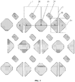
- One aspect of the present disclosure provides a pixel structure.
- the pixel structure provided in the present disclosure includes first sub-pixels 10, second sub-pixels 20, and third sub-pixels 30. Two opposing adjacent third sub-pixels 30 are arranged to face each other and form a third sub-pixel group 31.
- the second sub-pixels 20 are aligned in a row (e.g., the horizontal direction) to form second-sub-pixel rows.
- the first sub-pixels 10 and the third sub-pixel groups 31 are arranged in an alternating configuration in a row, e.g., one first sub-pixel 10 is arranged between two third sub-pixel groups 31, and vice versa.
- the second-sub-pixels rows and the rows formed by the first sub-pixels 10 and the third sub-pixel groups 31 are arranged in an alternating configuration, e.g., one second-sub-pixel row is arranged between two rows formed by the first sub-pixels 10 and the third sub-pixel groups 31, and vice versa.
- the two opposing adjacent third sub-pixels 30 may refer to the two adjacent third sub-pixels 30 arranged facing/opposing each other along a direction of the vertical axis between the two third sub-pixels 30.
- the two third sub-pixels 30 may have the closest distance in between.
- the sizes and shapes of the two third sub-pixels 30 may be substantially the same.
- the two third sub-pixels 30 may also have mirror symmetry, i.e., one of the third sub-pixel 30 is the mirror image of the other third sub-pixel 30. For example, if the two third sub-pixels 30 both move toward the center (along the horizontal axis in Figure 1 ) of the two third sub-pixels 30, the two third sub-pixels 30 may form a pattern with matching boundaries.
- the two third sub-pixels 30 for forming a third sub-pixel group 31 may also have different shapes and/or different sizes.
- one third sub-pixel 30 may have a greater size than the other third sub-pixel 30.
- the two third sub-pixels 30 may have similar overall shapes but may differentiate each other in some areas. For example, certain areas of the two third sub-pixels 30 may have been removed or modified such that the two third sub-pixels 30 may have similar overall shapes but different shapes in certain areas. Other reasons may also cause the two third sub-pixels 30 to have overall similar shapes but different shapes in certain areas.
- the two third sub-pixels 30 with the features described above are also suitable for the manufacturing/designing of the third sub-pixels 30 for forming the third sub-pixel group 31.
- the second sub-pixels 20 are aligned as second-sub-pixel columns (along the direction of a column axis).
- the first sub-pixels 10 and the third sub-pixel groups 31 are arranged in an alternating configuration in columns.
- one first sub-pixel 10 may be arranged between two third sub-pixel groups 31 in a column, and vice versa.
- the second-sub-pixel columns and the columns formed by the first sub-pixels 10 and the third sub-pixel groups 31 are arranged in an alternating configuration.
- one second-sub-pixel column may be arranged between two columns formed by the first sub-pixels 10 and the third sub-pixel groups 31, and vice versa.
- the geometric center of a second sub-pixel 20 is positioned on the perpendicular bisector of a line connecting the geometric centers of any two of the adjacent first sub-pixels 10 and third sub-pixel groups 31 (i.e., two first sub-pixels 10 and two third sub-pixel groups 31).
- the perpendicular bisector may refer to the line perpendicular to and passing through the midpoint of the line connecting the geometric centers of the two first sub-pixels 10/third sub-pixel groups 31.
- the geometric center of a second sub-pixel 20 may be positioned on the perpendicular bisector of the line connecting the adjacent first sub-pixel 10 and third sub-pixel group 31 in the row above the second sub-pixel 20.
- the geometric center of the second sub-pixel 20 is positioned on the perpendicular bisector of the line connecting the geometric centers of the adjacent first sub-pixel 10 and third sub-pixel group 31 in the row below the second sub-pixel 20. Also, the geometric center of the second sub-pixel 20 is positioned on the perpendicular bisector of the line connecting the geometric centers of the two adjacent first sub-pixels 10. Further, the geometric center of the second sub-pixel 20 is positioned on the perpendicular bisector of the line connecting the geometric centers of the adjacent first sub-pixel 10 and the adjacent third sub-pixel group 31 aligned along the column axis. Each of the adjacent first sub-pixels 10 is positioned in a diagonal direction with respect to the second sub-pixel 20.
- the line connecting the geometric center of the second sub-pixel 20 and either one of the adjacent first sub-pixels 10 may have an angle of 45 degrees clockwise or 135 degrees counter clockwise with respect to the direction of the row axis.
- the geometric center of the second sub-pixel 20 is positioned on the perpendicular bisector of the line connecting the geometric centers of the two adjacent third sub-pixel groups 31, where each of the adjacent third sub-pixel groups 31 is positioned in a diagonal direction with respect to the second sub-pixel 20.
- the line connecting the geometric center of the second sub-pixel 20 and either one of the adjacent third sub-pixel groups 31 may have an angle of 45 degrees clockwise or 135 degrees counter clockwise with respect to the direction of the row axis.
- the two second sub-pixels 20 with the closest distance may have the same shapes and each may be a mirror image of the other.
- Each of the two third sub-pixels 30 in one third sub-pixel group 31, positioned between two first sub-pixels 10, may be a mirror image of the other along the direction of the row axis or along the direction of the column axis.
- One third sub-pixels 30 positioned on one side of a first sub-pixel 10 may be a mirror image of the other third sub-pixel 30 on the other side of the first sub-pixel 10 along the direction of the row axis or along the direction of the column axis.
- the two adjacent third sub-pixels 30 facing/opposing each other along the direction of the row axis may form a third sub-pixel group 31.
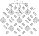
- the pixel structure of Figure 1 may be rotated for 90 degrees to form the pixel structure of Figure 2 .
- the two second sub-pixels 20 with the closest distance may have the same shapes and each may be a mirror image of the other.
- the two adjacent third sub-pixels 30 facing/opposing each other along the direction of the column axis may form a third sub-pixel group 31.
- the arrangement of the second sub-pixels 20 in the pixel structure of Figure 1 can be adjusted or modified.
- the two adjacent second sub-pixels 20 may have the same shapes, and a second sub-pixel 20 is positioned along a diagonal direction with respect to the adjacent first sub-pixels 10 and third sub-pixel groups 31.
- a second sub-pixel 20 with the closest distant to the second sub-pixel 20 along the diagonal direction may have the same orientation and relative position with respect to the adjacent first sub-pixels 10 and third sub-pixel groups 31.
- the pixel structure of Figure 3 may also be rotated for 90 degrees to form a new pixel structure. Details for rotating the pixel structure of Figure 3 are omitted herein.
- a pixel unit may include a second sub-pixel 20, an adjacent third sub-pixel 30 in a row adjacent to the second sub-pixel 20, and an adjacent first sub-pixel 10 in the row adjacent to the second sub-pixel 20.
- Same working principle and method for displaying the pixel structure can be applied on a plurality of embodiments such as the rotated pixel structure as shown in Figure 2 , and the pixel structure with a different arrangement of the second sub-pixels 20 as shown in Figure 3 .
- the same working principle and method for displaying can also be applied on the pixel structure with third sub-pixels 30 of a different shape in Figure 4 , and the pixel structure with sub-pixels for displaying different colors as shown in Figure 5 .
- a second sub-pixel 20, an adjacent third sub-pixel 30 in a row adjacent to the second sub-pixel 20, and an adjacent first sub-pixel 10 in the row adjacent to the second sub-pixel 20 may form a pixel unit.
- a second sub-pixel 20, an adjacent third sub-pixel 30 in a column adjacent to the second sub-pixel 20, and an adjacent first sub-pixel 10 in the column adjacent to the second sub-pixel 20 may form a pixel unit.
- Adjacent may refer to one sub-pixel being next to another sub-pixel in the upper or lower row of the one sub-pixel. Similarly, adjacent may also refer to one sub-pixel being next to another sub-pixel in the left or right column of the one sub-pixel.
- the pixel units in Figures 1 to 6 are marked in dashed boxes.
- Consecutive pixel units may form pixel unit rows along the direction of the row axis and pixel unit columns along the direction of the column axis. It should be noted that, the embodiments provided by the present disclosure are merely for exemplifying the arrangement of the pixel structures and should not limit the specific configuration of each pixel or sub-pixel.
- each pixel unit in the row may share a first sub-pixel 10 with an adjacent pixel unit in the same pixel unit row.
- each pixel unit in the column may share a first sub-pixel 10 with an adjacent pixel unit in the same pixel unit column. That is, a pixel unit positioned on the edges of the pixel panel may not share a first sub-pixel 10 with any adjacent pixel units.
- the left most first sub-pixel 10 in the first row formed by the first sub-pixels 10 and the third sub-pixel groups 31 may not be shared by two adjacent pixel units, and the left most first sub-pixel 10 in the second row formed by the first sub-pixels 10 and the third sub-pixel groups 31 may be shared by two adjacent pixel units.
- whether a first/last first sub-pixel 10 is shared by two adjacent pixel units may be dependent on the position of the first/last first sub-pixel 10 with respect to the first/last third sub-pixel 30 in the same row, i.e., whether the first/last element of the row is a first sub-pixel 10 or a third sub-pixel 30.
- the pixel structure provided by the present disclosure may include a first pixel unit 1 and a second pixel unit 2.
- the first pixel unit 1 may be adjacent to the second pixel unit 2.
- the first pixel unit 1 and the second pixel unit 2 may each include a first sub-pixel 10, a second sub-pixel 20, and a third sub-pixel 30.
- the first sub-pixel 10, share by the first pixel unit 1 and the second pixel unit 2, may display a single color.
- a third sub-pixel group 31 may include two third sub-pixels 30 opposing/facing each other.
- the third sub-pixel 30 of the first pixel unit 1 may be arranged on one side of the first sub-pixel 10, and the third sub-pixel 30 of the second pixel unit 2 may be arranged symmetrically on the other side of the first sub-pixel 10.
- the third sub-pixel 30 of the first pixel unit 1 and the third sub-pixel 30 of the second pixel unit 2 may be symmetrical along the direction of the row axis.
- the second sub-pixels 20 in the first pixel unit 1 and the second pixel units 2 may each be positioned along a diagonal direction with respect to the first sub-pixel 10 and the third sub-pixel 30 in the corresponding pixel unit.
- each of the two third sub-pixels 30 adjacent to the first sub-pixel 10, shared by the two pixel units, may form a third sub-pixel group 31 with the third sub-pixel 30 of the adjacent pixel unit.
- the two third sub-pixels 30 forming the third sub-pixel group 31 may be arranged symmetrically along the direction of the vertical axis between the two third sub-pixels 30.
- the third sub-pixel 30 of the pixel unit 2 may form a third sub-pixel group 31 with the third sub-pixel 30 of the adjacent pixel unit.
- the first sub-pixels 10 and the third sub-pixel groups 31 may be arranged in an alternating configuration in a row.
- first sub-pixel 10 may be arranged between two third sub-pixel groups 31 in a row, and vice versa.
- each second sub-pixel 20 may be positioned between the first sub-pixel 10 and a third sub-pixel group 31.
- the geometric center of a second sub-pixel 20 may be positioned at the intersection of the perpendicular bisector of the line connecting the geometric centers of the adjacent first sub-pixel 10 and third sub-pixel group 31 in the adjacent (i.e., upper or lower) row and the perpendicular bisector of the line connecting the geometric centers of the adjacent first sub-pixel 10 and third sub-pixel group 31 in the adjacent (i.e., left and right) column.
- the third sub-pixels 30 being arranged symmetrically may refer to the two third sub-pixels 30, having the same shapes and sizes, positioned on both sides of the vertical axis of the two third sub-pixels 30.
- the two third sub-pixels 30 may be completely symmetric to each other along the direction of the vertical axis.
- the two third sub-pixels 30 may be joined along the direction of the vertical axis to form a pattern of the third sub-pixel group 31 with matching boundaries.
- the R, G, and B colors described above may each be the color displayed by one sub-pixel.
- the colors described above may refer to the colors of the light-emitting layer of the organic electroluminescent diodes. When biased normally, the light-emitting layer may emit light with the corresponding color.
- the colors described above may refer to the colors of the CF (Color Filter) layer in the film substrate. When the backlight passes through the CF layer, the backlight is filter by the CF and light with the corresponding color can be displayed.
- geometric centers of the first sub-pixels 10 in consecutive rows and consecutive columns may be aligned to form lines along a diagonal direction different from the directions of the row axis and column axis.
- Geometric centers of the third sub-pixel groups 31 in consecutive rows and consecutive columns may be aligned to form lines along the diagonal direction different from the directions of the row axis and column axis.
- the lines, formed by the geometric centers of the first sub-pixels 10 along the diagonal direction may be parallel to the lines, formed by the geometric centers of the third sub-pixel groups 31 along the diagonal direction.
- the lines, formed by the geometric centers of the first sub-pixels 10 along the diagonal direction, and the lines, formed by the geometric centers of the third sub-pixel groups 31 along the diagonal direction, may be arranged in an alternating configuration such that one line formed by the geometric centers of the first sub-pixels 10 maybe arranged between two lines formed by the geometric centers of the third sub-pixels 31, and vice versa.
- the geometric center of a second sub-pixel 20 may be positioned at the intersection of the perpendicular bisector of the line connecting the geometric centers of the adjacent first sub-pixel 10 and third sub-pixel group 31 in the adjacent (i.e., upper or lower) row and the perpendicular bisector of the line connecting the geometric centers of the adjacent first sub-pixel 10 and sub-pixel group 31 in the adjacent (i.e., left and right) column.
- the two third sub-pixels 30 of one third sub-pixel group 31 may be arranged between two second sub-pixels 20 along a diagonal direction.
- the third sub-pixel 30 on one side of a second sub-pixel 20 and the third sub-pixel 30 on the other side of the second sub-pixel 20 may be centrosymmetric about the second sub-pixel 20.
- the first sub-pixels 10 may form lines along a diagonal direction
- the third sub-pixel groups 31 may form lines along a diagonal direction.
- a second sub-pixel 20 may be arranged between two first sub-pixels 10 and two third sub-pixel groups 31 such that the second sub-pixel 20 may be arranged between the two adjacent lines formed by the first sub-pixels 10 and between two adjacent lines formed by the third sub-pixel groups 31.
- Each of the two adjacent second sub-pixels 20 may be a mirror image of the other. That is, each of the two adjacent second sub-pixels 20 may be a mirror image of each other about the first sub-pixel 10 or the third sub-pixel group 31 between the two adjacent sub-pixels 20.
- the first sub-pixels 10 form consecutive lines along a diagonal direction
- the third sub-pixel groups 31 form consecutive lines along the diagonal direction.
- the lines formed by the first sub-pixels 10 are parallel to the lines formed by the third sub-pixel groups 31.
- the lines formed by the first sub-pixels 10 and the lines formed by the third sub-pixel groups 31 are arranged in an alternating configuration such that one line formed by the first sub-pixels 10 are arranged between two adjacent lines formed by the third sub-pixel groups 31, and vice versa.
- Each second sub-pixel 20 may be arranged between two adjacent first sub-pixels 10 and between two third sub-pixel groups 31.
- the two first sub-pixels 10 are arranged along a diagonal direction and the two third sub-pixel groups 31 are arranged in a diagonal direction. It should be understood that, it is only required that the line representing the closest distance between two adjacent sub-pixels aligned in a diagonal direction forms an acute angle (i.e., ranging between 0 degrees to 90 degrees) with the row axis (e.g., horizontal direction). In certain embodiments, the acute angle may be 45 degrees. An acute angle of 45 degrees may form more desirable distances between adjacent sub-pixels in the corresponding FMM.
- the manufacturing process for forming the pixel structure can be improved.
- the first sub-pixels 10 may be arranged in a diagonal direction with an acute angle of 45 degrees or 135 degrees with the row axis.
- the third sub-pixel groups 31 may be arranged in a diagonal direction with an acute angle of 45 degrees or 135 degrees with the row axis.
- the second sub-pixel 20 may be arranged in a diagonal direction of 45 degrees with respect to the first sub-pixel 10 and the third sub-pixel group 31.
- the second sub-pixel 20 may be arranged in a direction of 45 degrees along the upper or lower left direction of the first sub-pixel 10/third sub-pixel group 31, or the second sub-pixel 20 may be arranged in a direction of 45 degrees along the upper or lower right direction of the first sub-pixel 10/third sub-pixel group 31.
- the geometric centers of the first sub-pixels 10 in a same row/column may be along a same line.
- the geometric centers of the third sub-pixel groups 31 in a same row/column may be along a same line.
- the geometric centers of the second sub-pixels 20 in a same row/column may be along a same line.
- the above arrangement of sub-pixels may simplify the manufacturing process of the pixel structure.
- the geometric centers of the first sub-pixels 10, the geometric centers of the second sub-pixels 20, and the geometric centers of the third sub-pixel groups 31 may be positioned uniformly.
- the geometric centers of the first sub-pixels 10, the geometric centers of the second sub-pixels 20, and the geometric centers of the third sub-pixel groups 31 may be positioned uniformly.
- sub-pixels with different colors can be distributed in the display panel uniformly. Images displayed by the display panel can have improved display quality.
- the shape of the first sub-pixel 10, the second sub-pixel 20, and the third sub-pixel group 31 may each have axial symmetry.
- the symmetry axes of the first sub-pixels 10 and the symmetry axes of the third sub-pixel groups 31 may extend in a direction parallel to the direction of the row axis (as shown in Figures 1 to 5 ), parallel to the direction of the column axis (as shown in Figures 1 to 5 ), and/or parallel to a diagonal direction (as shown in Figures 1 to 5 ).
- the symmetry axes of the second sub-pixels 20 may extend in a direction parallel to the direction of the row axis (as shown in Figures 1 to 5 ), parallel to the direction of the column axis (as shown in Figures 1 to 5 ), and/or parallel to a diagonal direction (as shown in Figures 1 to 5 ).
- the symmetry axes of the third sub-pixel groups 31 and/or the symmetric axes of the third sub-pixels 30 may extend in a direction parallel to the direction of the row axis (as shown in Figures 1 to 4 ), or parallel to the direction of the column axis (as shown in Figures 1 to 4 ), and/or parallel to a diagonal direction (as shown in Figure 5 ).
- the first sub-pixels 10, the second sub-pixels 20, and the third sub-pixel groups 31 may form a structure with axes of symmetry.
- the FMM is often stretched along the direction of the row axis or along the direction of the column axis. Since the axes of symmetry of the sub-pixels may be arranged along the direction of the row axis, along the direction of the column axis, and/or along the diagonal direction, the stretching process may not deform the FMM.
- the positions of the sub-pixels in the pixel structure can remain accurate.
- the shape of the first sub-pixel 10, the third sub-pixel 30, the third sub-pixel group 31, and the second sub-pixel 20 may each be one of a circular shape, a triangular shape, a quadrilateral shape, a pentagonal shape, a hexagonal shape, and/or an octagonal shape.
- the shapes of the sub-pixels may be determined based on manufacturing/design requirements.
- the first sub-pixel 10 may have a quadrilateral shape or an octagonal shape
- the third sub-pixel 30 may have a triangular shape or a quadrilateral shape.
- Two adjacent third sub-pixels 30 may form the third sub-pixel group 31, and the overall shape of the third sub-pixel group 31 may be quadrilateral or octagonal.
- the second sub-pixel 20 may have a quadrilateral shape or an octagonal shape.
- the shapes of the sub-pixels can be determined flexibly based on the application, requirements on the display effect, etc.
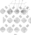
- a first sub-pixel 10 may have a rhombus shape
- a third sub-pixel 30 may have an isosceles triangle shape.
- a third sub-pixel group 31, formed by two adjacent third sub-pixels 30, may have an overall rhombus shape.
- a second sub-pixel 20 may have a rectangular shape.
- the pixel structure of Figure 5 may be modified from the pixel structure of Figure 1 .
- the first sub-pixel 10 may have a rhombus shape
- the third sub-pixel 30 may have a rectangular shape.
- the third sub-pixel group 31, formed by two adjacent third sub-pixels 30, may have an overall quadrilateral shape.
- the second sub-pixel 20 may have a rectangular shape.
- the shapes and arrangement of the sub-pixels in a pixel unit can have many variations according to manufacturing/design requirements.
- the shapes and arrangement of the sub-pixels can be determined flexibly according to the application of the display panel or according to the requirements from clients.
- certain angles of the sub-pixels may be chamfered.
- the turning angles of the rhombus may be chamfered.
- the apex angle of the isosceles triangle or the turning angles of the rectangle may be chamfered.
- the turning angles of the rectangle may be chamfered.
- the above shapes and arrangement of the sub-pixels may improve independent color display of the sub-pixels.
- the distance/spacing between any two sub-pixels may be adjusted or modified according to manufacturing/design requirements to ensure that the display panels, containing the sub-pixels, display colors and images accurately.
- the areas of the sub-pixels of the pixel structure described above can be determined below.
- the area of the first sub-pixel 10 may be the same as the area of the third sub-pixel group 31, and the area of the second sub-pixel 20 may be less than the area of the first sub-pixel 10.
- the area of the third sub-pixel group 31 may be less than the area of the first sub-pixel 10, and the area of the first sub-pixel 10 may be greater than the area of the second sub-pixel 20.
- the first sub-pixel 10, the second sub-pixel 20, and the third sub-pixel group 31 may each display any one of the red (R), green (G), and blue (B) colors such that the display panel can display full-color images.
- the first sub-pixels 10 may display R
- the second sub-pixels 20 may display G
- the third sub-pixel groups 31 may display B.
- the sub-pixels displaying R may be shared by adjacent pixel units
- the two sub-pixels displaying B may be adjacent to each other.
- the first sub-pixels 10 may display B
- the second sub-pixels 20 may display G
- the third sub-pixel groups 31 may display R.
- the two sub-pixels display R may be adjacent to each other
- the sub-pixels display B may be shared by adjacent pixel units.
- the pixel structure described above may be used in OLED display devices and/or LED devices. That is, the pixel structure in the embodiments of the present disclosure may be used in OLED display devices, LCD display devices, and/or other suitable devices containing pixel structures such as digital cameras, plasma display devices.
- the area of a sub-pixels for displaying blue may be larger than the area of a sub-pixel for displaying red and the area of a sub-pixel for displaying green.
- a sub-pixel for displaying green may have the smallest area. That is, the area of the second sub-pixel 20 may be smaller than the areas of both the first sub-pixel 10 and the third sub-pixel group 31.
- the sub-pixels for displaying green easier to be identified by human eye, may be distributed uniformly in the directions of row axis and column axis to ensure desirable display quality along the directions of row axis and column axis.
- the first sub-pixels 10, the second sub-pixels 20, and the third sub-pixel groups 31 may be formed through a patterning process.
- the first sub-pixels 10, the second sub-pixels 20, and the third sub-pixels 30 may be formed through a deposition process.
- the patterning process may include a photolithography process, or include a photolithography process and corresponding etching steps.
- the patterning process may also include printing, inkjet printing, and/or other process for forming predetermined patterns.
- the photolithography process may refer to the steps including film formation, exposure, and/or development. By applying appropriate photoresist, masks, and/or exposure apparatus, patterns can be formed through the photolithography process.
- the deposition process i.e., the vacuum coating process
- the deposition process may be referred as the process of evaporating/subliming the material/substance for forming the film and depositing the evaporated/sublimed material/substance on the surface of the substrate/device.
- the FMM can be applied on the surface of the substrate/device such that the evaporated/sublimed material/substance may not be formed in the areas covered by the FMM. Based on the pixel structure to be formed, appropriate processes can be selected to form the pattern of the pixel structure.
- the first sub-pixels 10, the second sub-pixels 20, and the third sub-pixel groups 31 may correspond to the openings in the FMM.
- the limit on the distance/spacing between two openings in the FMM may be applied on a diagonal direction (e.g., 45 degrees) to increase the density of the sub-pixels and improve the display resolution.
- the resolution of greater than 300 ppi (pixels per inch) can be achieved by embodiments of the present disclosure.
- the distance between two sub-pixels may represent the distance in a diagonal direction, the distance between to sub-pixels may be increased such that it is easier to apply FMM to form the pattern of sub-pixels.
- the pattern may correspond to the areas on the FMM with openings to form the sub-pixels.
- the distance/spacing between the openings (i.e., along a diagonal direction) in the FMM as described above may be much greater than the distance/spacing between the openings (i.e., along the row axis or column axis) in a conventional FMM.
- a pixel structure with higher resolution may be obtained.
- certain structures, e.g., the light emitting layer may be formed in one step. Independent display can be obtained by driving the sub-pixels independently.
- the arrangement/design as described above may further simplify the manufacturing process of the pixel structures and improve the display resolution by the pixel structure.
- the blue or red sub-pixel in one pixel unit may be adjacent to the blue or red sub-pixel in an adjacent pixel unit, i.e., the blue (or red) sub-pixel of one pixel unit is positioned adjacent to the blue (or red) sub-pixel of an adjacent pixel unit, two adjacent pixel units may share a first sub-pixel 10.
- five sub-pixels can have the same display effect as six sub-pixels.
- the arrangement described above may also reduce the areas between sub-pixels, i.e., the areas with no light emission, such that the aperture ratio can be increased, for example, to about 42%.
- the arrangement/configuration described above may ensure desirable aperture ratio.
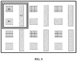
- the conventional pixel structure illustrated in Figure 7 often has a display resolution of 200 ppi and an aperture ratio of about 20% to about 30%
- the conventional pixel structure illustrated in Figure 8 often has a display resolution of 300 ppi and an aperture ratio of about 37%
- the conventional pixel structure illustrated in Figure 9 often has a display resolution of less than 300 ppi and an aperture ratio of about 30% to about 35%.
- B1 represents blue color
- G1 represents green color
- R1 represents red color.
- the disclosed pixel structure increases the density of sub-pixels and increases display resolution (e.g., often higher than 300 ppi).
- the sub-pixels for displaying blue may be next to the sub-pixels for displaying red, and areas between adjacent sub-pixels (i.e., the areas having no light illumination) can be reduced.
- the aperture ratio of the disclosed pixel structure can be about 42%.
- sub-pixels displaying green easier to be distinguished by human eyes, may be arranged/aligned uniformly in rows and in columns on the display panel, so that display quality along the horizontal direction and along the vertical direction may be ensured.
- five sub-pixels may have the same display effect as sixe sub-pixels.
- the display products can have improved product lifespan and display brightness.
- the distance between the two openings in the FMM corresponding to the sub-pixels for displaying the three primary colors may all be increased.
- the arrangement/configuration described above may make the design of FMM easier.
- the deposition process to form the organic layer may also be easier. Higher resolution can be easier to obtain. It is understandable that, compared to conventional pixel structures, as shown in Figures 7 to 9 , with three sub-pixels in one pixel unit, the pixel structure provided in the present disclosure can obtain the display effect of two pixel units (i.e., six sub-pixels) by only using five sub-pixels.
- the manufacturing process for forming the pixel structure can be greatly simplified, and the pixel structure can be easier to form by using the FMM.
- the pixel structures provided in the present disclosure may receive display data/information through data lines.
- the first sub-pixels 10, the second sub-pixels 20, and the third sub-pixels 30 may display colors independently.
- a first sub-pixel 10, a second sub-pixel 20, and a third sub-pixel 30 may each be connected to one data line to receive display data/information. Since a first sub-pixel 10 may be shared by a first pixel unit 1 and a second pixel unit 2, only one data line is required for one first sub-pixel 10 to be shared by two pixel units.
- five sub-pixels can obtain the same display effect of six sub-pixels.
- the number of data lines used in the pixel structure can be reduced accordingly and back panel wiring for the data lines can be easier.
- Embodiments of the present disclosure also provide a pixel structure.
- the line connecting the geometric centers of two adjacent sub-pixels of different colors may form an angle of 45 degrees with the horizontal line (i.e., the row axis).
- the angle of 45 degrees may represent an optimized design.
- the arrangement described above may enable five sub-pixels to have the display effect of six sub-pixels and improve the aperture ratio of the sub-pixels.
- the aperture ratio of the display device can be improved, and the display brightness of the pixel structure in a display device can also be improved accordingly.
- the lifespan of the OLED display panel that contains the pixel structure disclosed can be improved.
- a first sub-pixel may be shared by two adjacent pixel units, only one data line is required for one first sub-pixel.
- the number of data lines used in the pixel structure is reduced accordingly. Compared to conventional pixel structures, with the same number of pixel units used in a pixel structure, the number of data lines used in the pixel unit provided by the present disclosure may be fewer.
- the display device incorporating the pixel structure provided in the present disclosure may have lower power consumption.
- the pixel structure provided in the present disclosure may be suitable for manufacturing side-by-side top-emission AMOLED display panel.
- the side-by-side top-emission AMOLED display panel may be formed through a deposition process by applying the FMM on the surface of substrate/device.
- the present disclosure further provides a method for displaying the pixel structure described above.
- two adjacent pixel units share one first sub-pixel to display colors such that five sub-pixels can have the same display effect as six sub-pixels.
- the two adjacent pixel units can both display pixel information of the three colors (i.e., R, G, and B colors).
- a second sub-pixel 20, an adjacent third sub-pixel 30 in an adjacent row, and an adjacent first sub-pixel 10 in the adjacent row may form a pixel unit. Except for the first pixel unit and/or the last pixel unit in the odd rows (or even rows), each pixel unit may share the first sub-pixel 10 with an adjacent pixel unit in the same pixel unit row.
- the second sub-pixel 20, an adjacent third sub-pixel 30 in an adjacent column, and an adjacent first sub-pixel 10 in the adjacent column may form a pixel unit.
- each pixel unit may share the first sub-pixel 10 with an adjacent pixel unit in the same pixel unit column.
- each pixel unit can display pixel information of the three colors (i.e., R, G, and B colors).
- the pixel structure of Figure 6 may correspond to the pixel structure in Figure 1 .
- the sub-pixels for displaying red may be the first sub-pixels 10.
- the actual brightness value of a first sub-pixel 10, shared by the first pixel unit 1 and the adjacent second pixel unit 2 may be calculated as a weighted sum of the required theoretical brightness value of the red color displayed by the first sub-pixel 10 shared by the first pixel unit 1 and the required theoretical brightness value of the red color displayed by the first sub-pixel 10 shared by the second pixel unit 2.
- the actual brightness values of the sub-pixels of the pixel structures of Figures 2 to 4 can also be calculated using the method described above.
- the actual brightness value of the sub-pixels 10 for displaying blue in the pixel structure of Figure 5 can be calculated the same way as the actual brightness value for the sub-pixels 10 for displaying red in the pixel structure of Figure 1 .
- the first sub-pixel 10 shared by two adjacent pixel units may be labeled as R1 and R2.
- the R1 portion of the first sub-pixel 10 may be in the first pixel unit 10
- the R2 portion of the first sub-pixel 10 may be in the second pixel unit 20.
- the second sub-pixel 20 in the first pixel unit 1 may be labeled as G1, and the second sub-pixel 20 in the second pixel unit 2 may be labeled as G2.
- the third sub-pixel 30 in the first pixel unit 1 may be labeled as B1, and the third sub-pixel 30 in the second pixel unit 2 may be labeled as B2.
- the sub-pixels with the same labeling number i.e., 1 or 2
- R1, G1, and B1 may form a display color gamut.
- R2, G2, and B2 may form another display color gamut.
- the color of the display color gamut, formed by mixing the colors of the sub-pixels, may represent the display information of the display color gamut.
- a data source for providing the pixel display information may input/send pixel display information to each pixel unit.
- the pixel display information may include color information for displaying the R, G, and B colors.
- the method for displaying colors using the pixel structure may include the following steps.
- the pixel structure may obtain the theoretical brightness values from the pixel display information for the colors displayed by the first sub-pixel 10, the second sub-pixel 20, and the third sub-pixel 30 of each pixel unit.
- the pixel structure may obtain the theoretical brightness values from the pixel display information for the colors displayed by the first sub-pixel 10, the second sub-pixel 20, and the third sub-pixel 30 of the first pixel unit 1.
- the pixel structure may also obtain the theoretical brightness values from the pixel display information for the colors displayed by the first sub-pixel 10, the second sub-pixel 20, and the third sub-pixel 30 of the second pixel unit 2.
- a driving chip may separate, amplify, and correct the pixel display information to obtain display information for the three colors (R, G, and B colors).
- the driving chip may further obtain the brightness signals for the three colors through appropriate matrix transformation calculation.
- the brightness signals for the three colors may correspond to the theoretical brightness values of the three colors. Any suitable means for separating brightness information in conventional pixel structure manufacturing can be used to separate the brightness signals described above and the details are omitted herein.
- the pixel structure may calculate the actual brightness values of the first sub-pixel 10, the second sub-pixel 20, and the third sub-pixel 30 of each pixel unit.
- the pixel structure may calculate the actual brightness value of the first sub-pixel 10, the second sub-pixel 20, and the third sub-pixel 30 of the first pixel unit 1.
- the pixel structure may also calculate the actual brightness value of the first sub-pixel 10, the second sub-pixel 20, and the third sub-pixel 30 of the second pixel unit 2.
- the actual brightness value of the second sub-pixels 20 may be the theoretical brightness values of the color displayed by the second sub-pixels 20.
- the actual brightness values of the third sub-pixels 30 may also be the theoretical brightness value of the color displayed by the third sub-pixels 30.
- the actual brightness value of the first sub-pixel 10, shared by the first pixel unit 1 and the adjacent second pixel unit 2, can be calculated as a sum of the weighted theoretical brightness value of the color displayed by the first sub-pixel 10 in the first pixel unit 1 and the weighted theoretical brightness value of the color displayed by the first sub-pixel 10 in the second pixel unit 2.
- the input data signal to the first sub-pixel 10 may be a weighted sum of the pixel display data for the first sub-pixel 10 of the first pixel unit 1 and the pixel display data for the first sub-pixel 10 of the second pixel unit 2.
- the actual brightness value of the first sub-pixel 10 may be a sum of the weighted theoretical brightness values of the first sub-pixels 10 shared by adjacent pixel units.
- the weighted theoretical brightness value may represent the product of the theoretical brightness value and the relative weight corresponding to the theoretical brightness value.
- H represents the actual brightness value of the sub-pixel, i.e., the weighted sum.
- the relative weight corresponding to the theoretical brightness value of color displayed by the first sub-pixel 10 of the first pixel unit 1 may be 1/2.
- the relative weight corresponding to the theoretical brightness value of color displayed by the first sub-pixel 10 of the second pixel unit 1 may also be 1/2.
- a first sub-pixel 10 may display red or blue.
- the input signal to the first sub-pixel 10 may be a sum of the weighted pixel display information (i.e., red or blue) displayed by the first pixel 10 shared by the first pixel unit 1 and by the first pixel 10 shared by the second pixel unit 2.
- the weighted pixel display information may represent the product of the weighted pixel display information for red/blue color and the corresponding relative weight, where the relative weight is 1/2 for the first sub-pixel 10 of the first pixel unit 1 and for the first sub-pixel 10 of the second pixel unit 2. It should be understood that, the overall display effect of images (e.g., bright or dark), generated based on the pixel display information corresponding to the images, can be adjusted through adjusting the values of the relative weights. Desirable display brightness can be obtained by selecting suitable values of relative weights for generating desirable weighted sum.
- the pixel structure may input the corresponding actual brightness values into the first sub-pixel 10, the second sub-pixel 20, and the third sub-pixel 30 of each pixel unit to display images using the three primary colors (i.e., R, G, and B colors).
- step S3 the actual brightness values of the first sub-pixels 10, the second sub-pixels 20, and the third sub-pixels 30 may be outputted through step S2.
- the actual brightness values may be sent to the corresponding sub-pixels to display images.
- each sub-pixel may be connected to a data line.
- the actual brightness values of the first sub-pixels 10, the second sub-pixels 20, and the third sub-pixels 30, generated through step S2 may be sent/transported to the corresponding sub-pixels through the data lines connected to the sub-pixels.
- five sub-pixels can have the same display effect as six sub-pixels through simple a pixel sharing algorithm. Accordingly, the number of data lines used in the pixel structure can be reduced and back panel wiring for the data lines can be easier.
- the display apparatus contains the pixel structure as described above and the method for displaying the pixel structure.
- the display apparatus can be an LED panel, an electronic paper, an OLED display panel, a mobile phone, a tablet, a TV, a monitor, a laptop, a digital photo frame, a navigation device, or any product or device with display functions.
- the process for forming the pixel structure incorporated in the display apparatus may have higher manufacturing yield.
- the display apparatus may have improved display effect.
- the present disclosure provides a pixel structure and a method for displaying the pixel structure.
- higher aperture ratio and higher resolution can be obtained.
- the brightness of the pixel structure can be improved and the display effect of the display apparatus containing the pixel structure can be improved accordingly.
- the method for displaying the pixel structure can enable proper image display.
- Back panel wiring for the data lines may be easier and the power consumption of the display apparatus may be reduced.
- the pixel structure and method provided by the present disclosure provide a technical solution for the problems existing in conventional display apparatuses.
- the pixel structure and the method disclosed provide solution to overcome the difficulty in improving the display resolution in OLED display apparatuses due to limitations in the manufacturing process.
Landscapes
- Engineering & Computer Science (AREA)
- Physics & Mathematics (AREA)
- Computer Hardware Design (AREA)
- General Physics & Mathematics (AREA)
- Theoretical Computer Science (AREA)
- Manufacturing & Machinery (AREA)
- Chemical & Material Sciences (AREA)
- Crystallography & Structural Chemistry (AREA)
- Microelectronics & Electronic Packaging (AREA)
- Devices For Indicating Variable Information By Combining Individual Elements (AREA)
- Electroluminescent Light Sources (AREA)
- Liquid Crystal (AREA)
Claims (15)
- Structure de pixels comprenant des premiers sous-pixels (10), des deuxièmes sous-pixels (20) et des troisièmes sous-pixels (30), dans laquelle :deux troisièmes sous-pixels (30) adjacents se faisant face forment un groupe de troisièmes sous-pixels (31),les deuxièmes sous-pixels (20) sont agencés dans une rangée le long d'un premier axe afin de former des rangées de deuxièmes sous-pixels, les premiers sous-pixels (10) et les groupes de troisièmes sous-pixels (31) sont agencés dans une configuration en alternance le long d'une première direction du premier axe parallèle aux rangées de deuxièmes sous-pixels, et les rangées de deuxièmes sous-pixels et les rangées formées par les premiers sous-pixels (10) et les groupes de troisièmes sous-pixels (31) sont agencées dans une configuration en alternance ;les deuxièmes sous-pixels (20) sont agencés le long d'une deuxième direction d'un deuxième axe pour former des colonnes de deuxièmes sous-pixels, les premiers sous-pixels (10) et les groupes de troisièmes sous-pixels (31) sont agencés dans une configuration en alternance le long de la deuxième direction du deuxième axe parallèlement aux colonnes de deuxièmes sous-pixels, les colonnes de deuxièmes sous-pixels et des colonnes formées par les premiers sous-pixels (10) et les groupes de troisièmes sous-pixels (31) sont agencées dans une configuration en alternance ;
caractérisée en ce quele centre géométrique de chaque deuxième sous-pixel (20) est positionné sur une bissection perpendiculaire d'une ligne reliant deux centres, et les deux centres sont les deux centres quelconques des centres de groupes de troisièmes sous-pixels (31) adjacents au deuxième sous-pixels et des centres des premiers sous-pixels (10) adjacents au deuxième sous-pixel, où le premier axe est différent du deuxième axe ; etdans laquelle les deuxièmes sous-pixels et les premiers sous-pixels sont agencés dans une configuration en alternance le long d'une troisième direction pour former des premières lignes ;les deuxièmes sous-pixels et les groupes de troisièmes sous-pixels sont agencés dans une configuration en alternance le long de la troisième direction pour former des deuxièmes lignes ;les premières lignes et les deuxièmes lignes sont agencées dans une configuration en alternance ;une ligne représentant une distance la plus proche entre deux sous-pixels adjacents alignés le long de la troisième direction forme un angle aigu avec le premier axe ; etla troisième direction est différente de la première direction du premier axe et de la deuxième direction du deuxième axe. - Structure de pixels selon la revendication 1, dans laquelle :le deuxième sous-pixel, un groupe de troisièmes sous-pixels (31) adjacent dans une rangée adjacente, et un premier sous-pixel (10) adjacent dans la rangée adjacente forment une unité de pixels, des unités de pixels successives formant des rangées d'unités de pixels alignées le long de la première direction du premier axe, et excepté pour une unité de pixels à un bord de la rangée d'unités de pixels, chaque unité de pixels partageant le premier sous-pixel (10) avec une unité de pixels adjacente dans une même rangée d'unités de pixels ; oule deuxième sous-pixel, un groupe de troisièmes sous-pixels (31) adjacent dans une colonne adjacente, et un premier sous-pixel (10) adjacent dans la colonne adjacente forment une unité de pixels, des unités de pixels successives formant des colonnes d'unités de pixels alignées le long de la deuxième direction du deuxième axe, et excepté pour une unité de pixels à un bord de la colonne d'unités de pixels, chaque unité de pixels partage le premier sous-pixel (10) avec une unité de pixels adjacente dans une même colonne d'unités de pixels ; et de préférence,des centres géométriques des premiers sous-pixels (10) dans une rangée ou dans une colonne sont alignés dans une ligne droite ;des centres géométriques des groupes de troisièmes sous-pixels (31) dans une rangée ou dans une colonne sont alignés dans une ligne droite ; etdes centres géométriques des deuxièmes sous-pixels (20) dans une rangée ou dans une colonne sont alignés dans une ligne droite.
- Structure de pixels selon la revendication 1, dans laquelle :la troisième direction est à 45 degrés dans le sens des aiguilles d'une montre par rapport à la première direction du premier axe, à 45 degrés dans le sens inverse des aiguilles d'une montre par rapport à la première direction du premier axe, à 45 degrés dans le sens des aiguilles d'une montre par rapport à la deuxième direction du deuxième axe, ou à 45 degrés dans le sens inverse des aiguilles d'une montre par rapport à la deuxième direction du deuxième axe ;des centres géométriques des premiers sous-pixels (10) dans des rangées successives ou des colonnes successives sont alignés pour former des premières lignes le long de la troisième direction ;des centres géométriques des groupes de troisièmes sous-pixels (31) dans des rangées successives ou des colonnes successives sont alignés pour former des deuxièmes lignes le long de la troisième direction ;chaque deuxième sous-pixel (20) est aligné entre deux premiers sous-pixels (10) adjacents ou entre deux groupes de troisièmes sous-pixels (31) adjacents ; où deux premiers sous-pixels (10) adjacents sont alignés dans la troisième direction et les deux groupes de troisièmes sous-pixels (31) adjacents sont alignés dans une quatrième direction perpendiculaire à la troisième direction ; etun centre géométrique de chaque deuxième sous-pixel (20) est agencé à une intersection d'une bissection perpendiculaire d'une ligne reliant des centres géométriques d'un premier sous-pixel (10) adjacent et d'un groupe de troisièmes sous-pixels (31) dans une rangée adjacente et une bissection perpendiculaire d'une ligne reliant des centres géométriques d'un premier sous-pixel (10) adjacent et d'un groupe de troisièmes sous-pixels (31) dans une colonne adjacente ;de préférence,chacun parmi les deux troisièmes sous-pixels (30) dans un groupe de troisièmes sous-pixels (31) est une image miroir des autres le long de la première direction du premier axe, ou le long de la deuxième direction du deuxième axe, chaque groupe de troisièmes sous-pixels (31) étant agencé entre deux premiers sous-pixels (10) le long de la première direction du premier axe ou le long de la deuxième direction du deuxième axe, et deux troisièmes sous-pixels (30) adjacents étant agencés sur deux côtés du premier sous pixel, où chacun des deux troisièmes sous-pixels (30) adjacents a une distance la plus courte jusqu'au premier sous-pixel (10) le long de la première direction du premier axe ou le long de la deuxième direction du deuxième axe, de sorte que deux troisièmes sous-pixels (30) adjacents possèdent une symétrie miroir, une centrosymétrie, ou une combinaison d'une symétrie miroir et d'une centrosymétrie, autour d'un centre géométrique du premier sous-pixel, ouchaque groupe de troisièmes sous-pixels (31) est agencé entre deux deuxièmes sous-pixels (20) adjacents le long de la troisième direction de sorte que chaque deuxième sous-pixel (20) est agencé entre deux groupes de troisièmes sous-pixels (31) adjacents le long de la troisième direction, les deux troisièmes sous-pixels (30) adjacents ayant une symétrie miroir, une centrosymétrie ou une combinaison d'une symétrie miroir et d'une centrosymétrie, autour d'un centre géométrique du deuxième sous-pixel ;
de préférence,une forme du premier sous-pixel, une forme du groupe de troisièmes sous-pixels et une forme du deuxième sous-pixel (20) a chaque fois un axe de symétrie ; etun axe de symétrie de la forme du premier sous-pixel (10) s'étend le long d'une direction parallèle à un axe parmi le premier axe, le deuxième axe et un axe diagonal, un axe de symétrie de la forme du groupe de troisièmes sous-pixels (31) s'étend le long d'une direction parallèle à un axe parmi le premier axe, le deuxième axe et l'axe diagonal, et un axe de symétrie de la forme du deuxième sous-pixel (20) s'étend le long d'une direction parallèle à un axe parmi le premier axe, le deuxième axe et l'axe diagonal ;
et de préférence,les premières lignes formées par les centres géométriques des premiers sous-pixels (10) sont agencées le long d'une direction de 45 degrés ou de 135 degrés par rapport au premier axe ; etles deuxièmes lignes formées par les centres géométriques des groupes de troisièmes sous-pixels (31) sont agencées le long d'une direction de 45 degrés ou de 135 degrés par rapport au premier axe. - Structure de pixels selon la revendication 1, dans laquelle :chacune parmi la forme du premier sous-pixel, la forme du troisième sous-pixel, la forme du groupe de troisièmes sous-pixels, et la forme du deuxième sous-pixel (20) est une forme circulaire, une forme triangulaire, une forme quadrilatérale, une forme pentagonale, une forme hexagonale, une forme octogonale ou une combinaison de celles-ci,de préférence,le premier sous-pixel (10) a une forme quadrilatérale ou une forme octogonale ;le troisième sous-pixel (30) a une forme triangulaire ou une forme quadrilatérale de sorte que le groupe de troisièmes sous-pixels (31) formé par deux troisièmes sous-pixels (30) adjacents se faisant face a une forme quadrilatérale ou une forme octogonale ; etle deuxième sous-pixel (20) a une forme quadrilatérale ou une forme octogonale.
- Structure de pixels selon la revendication 4, dans laquelle :le premier sous-pixel (10) a une forme de losange ;le troisième sous-pixel (30) a une forme rectangulaire de sorte que le groupe de troisièmes sous-pixels (31) formé par deux troisièmes sous-pixels (30) adjacents se faisant face a une forme globale de quadrilatère ; etle deuxième sous-pixel (20) a une forme rectangulaire.
- Structure de pixels selon la revendication 4, dans laquelle :le premier sous-pixel (10) a une forme de losange ;le troisième sous-pixel (30) a une forme de triangle isocèle de sorte que le groupe de troisièmes sous-pixels (31) formé par deux troisièmes sous-pixels (30) adjacents se faisant face a une forme globale de losange ; etle deuxième sous-pixel (20) a une forme rectangulaire.
- Structure de pixels selon la revendication 4, dans laquelle :
des coins de la forme quadrilatère et de la forme octogonale sont chanfreinés. - Structure de pixels selon la revendication 4, dans laquelle :deux deuxièmes sous-pixels (20) adjacents ayant une distance la plus proche le long de la première direction du premier axe ou de la deuxième direction du deuxième axe ont des formes identiques, oudeux deuxièmes sous-pixels (20) adjacents ayant une distance la plus proche le long de la première direction du premier axe ou de la deuxième direction du deuxième axe ont une symétrie miroir autour d'une bissection perpendiculaire d'une ligne reliant des centres géométriques de deux deuxièmes sous-pixels (20) adjacents.
- Structure de pixels selon la revendication 1, dans laquelle :une surface du premier sous-pixel (10) est identique à une surface du groupe de troisièmes sous-pixels, et une surface du deuxième sous-pixel (20) est inférieure à la surface du premier sous-pixel ;éventuellement, une surface du groupe de troisièmes sous-pixels (31) est supérieure à une surface du premier sous-pixel, et la surface du premier sous-pixel (10) est supérieure à une surface d'un deuxième sous-pixel.
- Structure de pixels selon la revendication 1, dans laquelle :des centres géométriques des premiers sous-pixels (10), des centres géométriques des deuxièmes sous-pixels (20) et des centres géométriques des groupes de troisièmes sous-pixels (31) sont distribués de manière uniforme.
- Structure de pixels selon l'une quelconque des revendications 1 à 10, dans laquelle :les premiers pixels affichent une couleur rouge ou une couleur bleue, les deuxièmes sous-pixels (20) affichent une couleur verte, et les groupes de troisièmes sous-pixels (31) affichent une couleur bleue ou une couleur rouge,de préférence,chacun parmi le premier sous-pixel, le deuxième sous-pixel et le groupe de troisièmes sous-pixels (31) est relié à une ligne de données pour recevoir une information d'affichage de pixels.
- Procédé d'affichage de la structure de pixels selon l'une quelconque des revendications 1 à 11, dans lequel :le deuxième sous-pixel, un troisième sous-pixel (30) adjacent dans une rangée adjacente, et un premier sous-pixel (10) adjacent dans la rangée adjacente forment une unité de pixels, des unités de pixels successives formant des rangées d'unités de pixels alignées le long de la première direction du premier axe, et excepté pour une unité de pixels à un bord de la rangée d'unités de pixels, chaque unité de pixels partageant le premier sous-pixel (10) avec une unité de pixels adjacente dans une même rangée d'unités de pixels, de sorte que chaque unité de pixels affiche une information d'affichage de pixels de trois couleurs d'affichage, oule deuxième sous-pixel, un troisième sous-pixel (30) adjacent dans une colonne adjacente, et un premier sous-pixel (10) adjacent dans la colonne adjacente forment une unité de pixels, des unités de pixels successives formant des colonnes d'unités de pixels alignées le long de la deuxième direction du deuxième axe, et excepté pour une unité de pixels à un bord de la colonne d'unités de pixels, chaque unité de pixels partageant le premier sous-pixel (10) avec une unité de pixels adjacente dans une même colonne d'unités de pixels, de sorte que chaque unité de pixels affiche une information d'affichage de pixels des trois couleurs d'affichage.
- Procédé selon la revendication 12, comprenant en outre des étapes :étape S1, d'obtention de valeurs de brillance théoriques à partir de l'information d'affichage de pixels pour des couleurs affichées par le premier sous-pixel, le deuxième sous-pixel et le troisième sous-pixel (30) de chaque unité de pixels ;étape S2, de calcul de valeurs de brillance réelles du premier sous-pixel, du deuxième sous-pixel et du troisième sous-pixel (30) de chaque unité de pixels ; etétape S3, de prise en compte des valeurs de brillance réelles correspondantes dans le premier sous-pixel, le deuxième sous-pixel et le troisième sous-pixel (30) de chaque unité de pixels pour afficher des images.
- Procédé selon la revendication 13, dans lequel :la valeur de brillance réelle de la couleur affichée par les deuxièmes sous-pixels (20) est une valeur de brillance théorique affichée par le deuxième sous-pixel ;la valeur de brillance réelle de la couleur affichée par le troisième sous-pixel (30) est une valeur de brillance théorique affichée par le troisième sous-pixel ; etla valeur de brillance réelle de la couleur affichée par le premier sous-pixel (10) est calculée sous la forme d'une somme d'une valeur de brillance pondérée de la couleur affichée par une première partie du premier sous-pixel (10) et une valeur de brillance pondérée de couleur affichée par une deuxième partie du premier sous-pixel, où la première partie du premier sous-pixel est dans une première unité de pixels (1) et la deuxième partie du premier sous-pixel (110) est dans une deuxième unité de pixels (2) adjacente à la première unité de pixels (1) ;de préférence,une valeur de pondération relative multipliée par la valeur de brillance de la couleur affichée par la première partie du premier sous-pixel (10) est ½ ; etune valeur de pondération relative multipliée par la valeur de brillance de la couleur affichée par la deuxième partie du premier sous-pixel (10) est ½.
- Appareil d'affichage incluant une structure de pixels selon l'une quelconque des revendications 1 à 11, de préférence, l'appareil d'affichage est un dispositif d'affichage OLED, un dispositif LCD.
Applications Claiming Priority (2)
| Application Number | Priority Date | Filing Date | Title |
|---|---|---|---|
| CN201410842321.6A CN104465714B (zh) | 2014-12-30 | 2014-12-30 | 一种像素结构及其显示方法、显示装置 |
| PCT/CN2015/087027 WO2016107188A1 (fr) | 2014-12-30 | 2015-08-14 | Structure de pixels, son procédé d'affichage et afficheur |
Publications (3)
| Publication Number | Publication Date |
|---|---|
| EP3241236A1 EP3241236A1 (fr) | 2017-11-08 |
| EP3241236A4 EP3241236A4 (fr) | 2018-07-25 |
| EP3241236B1 true EP3241236B1 (fr) | 2022-04-06 |
Family
ID=52911490
Family Applications (1)
| Application Number | Title | Priority Date | Filing Date |
|---|---|---|---|
| EP15851646.8A Active EP3241236B1 (fr) | 2014-12-30 | 2015-08-14 | Structure de pixels, son procédé d'affichage et afficheur |
Country Status (6)
| Country | Link |
|---|---|
| US (1) | US10043433B2 (fr) |
| EP (1) | EP3241236B1 (fr) |
| JP (1) | JP6657127B2 (fr) |
| KR (1) | KR101898366B1 (fr) |
| CN (1) | CN104465714B (fr) |
| WO (1) | WO2016107188A1 (fr) |
Families Citing this family (95)
| Publication number | Priority date | Publication date | Assignee | Title |
|---|---|---|---|---|
| CN104885141B (zh) | 2013-11-04 | 2018-03-16 | 深圳云英谷科技有限公司 | 显示器子像素排布及其渲染方法 |
| CN104465714B (zh) | 2014-12-30 | 2017-04-26 | 京东方科技集团股份有限公司 | 一种像素结构及其显示方法、显示装置 |
| CN104466007B (zh) | 2014-12-30 | 2017-05-03 | 京东方科技集团股份有限公司 | 一种像素结构及其显示方法、显示装置 |
| CN104599625B (zh) * | 2015-03-02 | 2017-06-06 | 京东方科技集团股份有限公司 | 边界判定方法和装置、显示驱动方法和装置 |
| CN104992959B (zh) * | 2015-06-04 | 2018-02-13 | 信利(惠州)智能显示有限公司 | Oled像素排列结构及显示装置 |
| CN104952412B (zh) * | 2015-07-15 | 2018-04-13 | 深圳市华星光电技术有限公司 | 液晶面板的驱动方法及驱动装置 |
| CN105096856B (zh) * | 2015-07-23 | 2018-03-20 | 深圳市华星光电技术有限公司 | 液晶面板的驱动方法及驱动装置 |
| CN104992688B (zh) * | 2015-08-05 | 2018-01-09 | 京东方科技集团股份有限公司 | 像素阵列、显示装置及其驱动方法和驱动装置 |
| CN106486513B (zh) * | 2015-08-31 | 2023-09-29 | 昆山国显光电有限公司 | 像素结构以及oled显示面板 |
| CN106486514B (zh) * | 2015-08-31 | 2023-12-01 | 昆山国显光电有限公司 | 像素结构以及oled显示面板 |
| KR102401983B1 (ko) * | 2015-09-30 | 2022-05-25 | 엘지디스플레이 주식회사 | 투명표시장치 및 투명표시패널 |
| CN105529353A (zh) * | 2015-12-25 | 2016-04-27 | 昆山国显光电有限公司 | 显示器及其像素结构 |
| CN106935616B (zh) * | 2015-12-30 | 2019-09-17 | 昆山工研院新型平板显示技术中心有限公司 | Amoled显示屏及精密金属掩膜板 |
| US11233096B2 (en) | 2016-02-18 | 2022-01-25 | Boe Technology Group Co., Ltd. | Pixel arrangement structure and driving method thereof, display substrate and display device |
| CN107644888B (zh) * | 2016-07-22 | 2025-01-10 | 京东方科技集团股份有限公司 | 像素排列结构、显示基板、显示装置、制作方法及掩膜版 |
| US11448807B2 (en) | 2016-02-18 | 2022-09-20 | Chengdu Boe Optoelectronics Technology Co., Ltd. | Display substrate, fine metal mask set and manufacturing method thereof |
| CN110137213B (zh) | 2018-02-09 | 2025-03-25 | 京东方科技集团股份有限公司 | 像素排列结构及其显示方法、显示基板 |
| CN110134353B (zh) | 2018-02-09 | 2021-04-27 | 京东方科技集团股份有限公司 | 颜色补偿方法、补偿装置以及显示装置 |
| CN110137215B (zh) * | 2018-02-09 | 2025-01-14 | 京东方科技集团股份有限公司 | 像素排列结构、显示基板和显示装置 |
| US11747531B2 (en) | 2016-02-18 | 2023-09-05 | Chengdu Boe Optoelectronics Technology Co., Ltd. | Display substrate, fine metal mask set and manufacturing method thereof |
| US11264430B2 (en) * | 2016-02-18 | 2022-03-01 | Chengdu Boe Optoelectronics Technology Co., Ltd. | Pixel arrangement structure with misaligned repeating units, display substrate, display apparatus and method of fabrication thereof |
| CN107275359B (zh) * | 2016-04-08 | 2021-08-13 | 乐金显示有限公司 | 有机发光显示装置 |
| CN105957488B (zh) * | 2016-07-11 | 2018-05-01 | 京东方科技集团股份有限公司 | 像素阵列及其驱动方法、显示面板及显示装置 |
| US20180053811A1 (en) * | 2016-08-22 | 2018-02-22 | Emagin Corporation | Arrangement of color sub-pixels for full color oled and method of manufacturing same |
| CN106157818B (zh) * | 2016-09-05 | 2022-06-24 | 京东方科技集团股份有限公司 | 一种柔性显示面板、其制作方法及显示装置 |
| US11437451B2 (en) | 2016-09-22 | 2022-09-06 | Emagin Corporation | Large area display and method for making same |
| CN107968103B (zh) * | 2016-10-20 | 2020-03-17 | 昆山国显光电有限公司 | 像素结构及其制造方法、显示装置 |
| KR102725326B1 (ko) * | 2016-12-21 | 2024-11-01 | 엘지디스플레이 주식회사 | 유기 발광 다이오드 표시 장치 |
| CN108807460B (zh) * | 2017-04-28 | 2019-08-23 | 昆山国显光电有限公司 | 像素结构驱动方法 |
| CN107293571B (zh) * | 2017-06-09 | 2019-09-20 | 深圳市华星光电技术有限公司 | Oled显示面板的像素排列结构及oled显示面板 |
| JP7015324B2 (ja) | 2017-08-31 | 2022-02-02 | クンシャン ゴー-ビシオノクス オプト-エレクトロニクス カンパニー リミテッド | ピクセル構造、oledディスプレイデバイス、および駆動方法 |
| CN109427851B (zh) | 2017-08-31 | 2021-04-23 | 昆山国显光电有限公司 | 像素结构、oled显示屏以及蒸镀掩膜版 |
| CN108510895B (zh) * | 2017-08-31 | 2019-05-03 | 昆山国显光电有限公司 | 像素结构、掩膜版及显示装置 |
| CN109427265B (zh) * | 2017-08-31 | 2020-10-16 | 昆山国显光电有限公司 | 像素驱动方法 |
| WO2019042048A1 (fr) | 2017-08-31 | 2019-03-07 | 昆山国显光电有限公司 | Structure de pixels, masque et dispositif d'affichage |
| CN107610594A (zh) * | 2017-09-19 | 2018-01-19 | 厦门天马微电子有限公司 | 一种显示面板和显示装置 |
| US10283086B1 (en) * | 2017-11-06 | 2019-05-07 | Novatek Microelectronics Corp. | Display device with novel sub-pixel configuration |
| CN107942565B (zh) * | 2017-11-30 | 2021-03-26 | 厦门天马微电子有限公司 | 一种显示基板、显示面板及其显示装置 |
| US10607534B2 (en) | 2017-12-29 | 2020-03-31 | Wuhan China Star Optoelectronics Semiconductor Display Technology Co., Ltd. | OLED pixel arrangement structure having sub-pixels of different colors alternately arranged in adjacent rows and display panel including same |
| CN108198840B (zh) * | 2017-12-29 | 2020-12-29 | 武汉华星光电半导体显示技术有限公司 | 有机发光二极管像素排列结构及显示面板 |
| CN109994505B (zh) | 2018-01-02 | 2025-04-15 | 京东方科技集团股份有限公司 | 一种像素排布结构及相关装置 |
| CN108154848B (zh) * | 2018-01-19 | 2020-11-17 | 昆山国显光电有限公司 | 像素排列的显示方法、装置及显示设备 |
| CN110097862B (zh) * | 2018-01-31 | 2022-09-13 | 天马日本株式会社 | 显示装置及相对亮度数据的转换方法 |
| US11889719B2 (en) * | 2018-02-01 | 2024-01-30 | Wuhan China Star Optoelectronics Semiconductor Display Technology Co., Ltd. | Display panel |
| US11574960B2 (en) | 2018-02-09 | 2023-02-07 | Boe Technology Group Co., Ltd. | Pixel arrangement structure, display substrate, display device and mask plate group |
| CN114355678B (zh) | 2018-02-09 | 2023-11-03 | 京东方科技集团股份有限公司 | 显示基板和显示装置 |
| CN110137209A (zh) * | 2018-02-09 | 2019-08-16 | 京东方科技集团股份有限公司 | 一种像素排布结构、高精度金属掩模板及显示装置 |
| CN110137212B (zh) * | 2018-02-09 | 2022-05-27 | 京东方科技集团股份有限公司 | 像素排列结构、显示基板以及显示装置 |
| GB2571578B (en) * | 2018-03-02 | 2021-07-28 | Flexenable Ltd | Display device |
| CN110619813B (zh) * | 2018-06-20 | 2021-05-14 | 京东方科技集团股份有限公司 | 显示基板、其驱动方法、显示装置及高精度金属掩模版 |
| WO2019242510A1 (fr) | 2018-06-20 | 2019-12-26 | 京东方科技集团股份有限公司 | Substrat d'affichage et son procédé de commande, et dispositif d'affichage |
| CN110660823A (zh) * | 2018-06-29 | 2020-01-07 | 京东方科技集团股份有限公司 | 显示基板、其显示方法、显示装置及高精度金属掩模板 |
| CN109244109B (zh) * | 2018-08-30 | 2021-02-26 | 武汉华星光电半导体显示技术有限公司 | 像素结构和显示装置 |
| CN108877553A (zh) * | 2018-09-11 | 2018-11-23 | 华域视觉科技(上海)有限公司 | 车辆弱交互显示装置 |
| CN109256077B (zh) * | 2018-11-01 | 2021-12-14 | 京东方科技集团股份有限公司 | 显示面板的控制方法、装置及可读存储介质 |
| CN113823240B (zh) * | 2018-12-13 | 2023-04-18 | 京东方科技集团股份有限公司 | 显示装置 |
| CN111384086B (zh) * | 2018-12-28 | 2023-04-18 | 广东聚华印刷显示技术有限公司 | 像素结构及显示屏 |
| CN111383542A (zh) * | 2018-12-29 | 2020-07-07 | 广东聚华印刷显示技术有限公司 | 像素结构和显示面板 |
| CN112074895B (zh) * | 2019-01-11 | 2022-06-03 | 京东方科技集团股份有限公司 | 像素排列结构、显示基板及显示装置 |
| KR102759269B1 (ko) | 2019-01-24 | 2025-01-24 | 보에 테크놀로지 그룹 컴퍼니 리미티드 | 픽셀 배열 구조, 디스플레이 패널 및 디스플레이 장치 |
| CN109817685B (zh) * | 2019-02-01 | 2021-05-07 | 武汉华星光电半导体显示技术有限公司 | Oled像素结构及显示装置 |
| KR102866754B1 (ko) | 2019-03-04 | 2025-09-30 | 삼성디스플레이 주식회사 | 표시 장치, 표시 장치의 제조장치 및 표시 장치의 제조방법 |
| CN111697025B (zh) * | 2019-03-12 | 2023-11-17 | 上海和辉光电股份有限公司 | Oled显示器件、显示面板、显示装置以及制造方法 |
| CN110098239B (zh) * | 2019-05-17 | 2021-11-02 | 京东方科技集团股份有限公司 | 像素结构、显示基板、掩模板及蒸镀方法 |
| CN111969114B (zh) | 2019-05-20 | 2022-04-12 | 京东方科技集团股份有限公司 | 显示面板、制造显示面板的方法和掩模板 |
| EP4006982A4 (fr) | 2019-07-31 | 2022-08-03 | BOE Technology Group Co., Ltd. | Substrat d'affichage et dispositif d'affichage |
| CN118843353A (zh) | 2019-07-31 | 2024-10-25 | 京东方科技集团股份有限公司 | 显示基板及其制备方法、显示面板、显示装置 |
| CN110610962B (zh) * | 2019-08-20 | 2021-02-26 | 深圳市华星光电半导体显示技术有限公司 | 透明显示面板 |
| CN110783390B (zh) * | 2019-10-31 | 2023-02-24 | 武汉天马微电子有限公司 | 一种显示面板及显示装置 |
| CN110690266A (zh) * | 2019-10-31 | 2020-01-14 | 广州番禺职业技术学院 | 一种像素结构及其渲染方法、显示装置 |
| CN112750863A (zh) * | 2019-10-31 | 2021-05-04 | 京东方科技集团股份有限公司 | 显示背板、掩膜版组件和显示装置 |
| CN117098422A (zh) | 2019-11-07 | 2023-11-21 | 华为技术有限公司 | 一种显示面板和电子设备 |
| EP3836222A3 (fr) | 2019-12-10 | 2021-08-04 | Samsung Display Co., Ltd. | Dispositif d'affichage, ensemble masque, et appareil de fabrication d'un dispositif d'affichage |
| US11557635B2 (en) | 2019-12-10 | 2023-01-17 | Samsung Display Co., Ltd. | Display device, mask assembly, and apparatus for manufacturing the display device |
| CN111261678B (zh) * | 2020-01-13 | 2023-07-25 | 昆山云英谷电子科技有限公司 | 显示器子像素排布及其渲染方法 |
| CN112436032B (zh) * | 2020-07-01 | 2022-10-18 | 昆山国显光电有限公司 | 显示面板及显示装置 |
| CN111969020B (zh) * | 2020-08-25 | 2023-04-25 | 维信诺科技股份有限公司 | 像素排布结构、显示面板及掩模版组 |
| CN111951728B (zh) * | 2020-08-28 | 2022-06-03 | 京东方科技集团股份有限公司 | 像素结构、显示面板、显示装置及制造、显示方法 |
| EP4213212A4 (fr) * | 2020-09-10 | 2025-01-15 | BOE Technology Group Co., Ltd. | Matrice de pixels et dispositif d'affichage |
| US12302730B2 (en) | 2020-09-29 | 2025-05-13 | Chengdu Boe Optoelectronics Technology Co., Ltd. | Pixel array and display device |
| CN112436048A (zh) | 2020-12-01 | 2021-03-02 | 京东方科技集团股份有限公司 | 像素结构、精细金属掩膜板、显示装置和控制方法 |
| KR102853688B1 (ko) * | 2020-12-18 | 2025-09-03 | 삼성디스플레이 주식회사 | 표시 장치 |
| CN116635926B (zh) * | 2020-12-29 | 2025-07-29 | 夏普株式会社 | 显示装置 |
| CN113130619B (zh) * | 2021-05-31 | 2023-04-07 | 京东方科技集团股份有限公司 | 一种显示基板、显示面板及显示装置 |
| CN113299727B (zh) * | 2021-06-25 | 2025-09-19 | 京东方科技集团股份有限公司 | 一种像素排列结构及显示装置 |
| CN113327972B (zh) * | 2021-07-01 | 2025-07-22 | 武汉天马微电子有限公司 | 显示面板、制备方法和显示装置 |
| CN114156332B (zh) * | 2021-12-13 | 2025-12-23 | 昆山国显光电有限公司 | 像素排布结构、显示面板和显示装置 |
| CN114388598A (zh) * | 2021-12-16 | 2022-04-22 | Tcl华星光电技术有限公司 | 显示面板和显示装置 |
| CN114512521A (zh) * | 2022-02-10 | 2022-05-17 | 合肥维信诺科技有限公司 | 像素排布结构、显示面板及显示装置 |
| CN116917976A (zh) * | 2022-02-18 | 2023-10-20 | 京东方科技集团股份有限公司 | 像素结构、显示基板及显示装置 |
| TWI801179B (zh) * | 2022-03-23 | 2023-05-01 | 友達光電股份有限公司 | 顯示裝置 |
| CN117255584A (zh) | 2022-06-06 | 2023-12-19 | 上海和辉光电股份有限公司 | 像素阵列、显示面板和金属掩膜板 |
| CN118434211A (zh) * | 2023-02-01 | 2024-08-02 | 台州观宇科技有限公司 | 显示设备及其制造方法 |
| CN119277919A (zh) * | 2024-09-24 | 2025-01-07 | 京东方科技集团股份有限公司 | 显示面板及显示装置 |
| CN120583854B (zh) * | 2025-07-30 | 2025-12-16 | 合肥维信诺科技有限公司 | 像素排布结构、显示面板和显示装置 |
Family Cites Families (55)
| Publication number | Priority date | Publication date | Assignee | Title |
|---|---|---|---|---|
| US1624708A (en) | 1927-01-25 | 1927-04-12 | James C Harris | Toy gun |
| US4458175A (en) * | 1977-04-13 | 1984-07-03 | Weekley Robert R | Mosaic additive reflectance color display screen |
| GB8622715D0 (en) * | 1986-09-20 | 1986-10-29 | Emi Plc Thorn | Display device |
| US5579027A (en) * | 1992-01-31 | 1996-11-26 | Canon Kabushiki Kaisha | Method of driving image display apparatus |
| FR2703814B1 (fr) * | 1993-04-08 | 1995-07-07 | Sagem | Afficheur matriciel en couleurs. |
| AUPM440494A0 (en) * | 1994-03-11 | 1994-04-14 | Canon Information Systems Research Australia Pty Ltd | Intermingling subpixels in discrete level displays |
| US6023315A (en) * | 1995-07-04 | 2000-02-08 | Sharp Kabushiki Kaisha | Spatial light modulator and directional display |
| JPH08335060A (ja) * | 1996-06-28 | 1996-12-17 | Mitsubishi Electric Corp | マトリクス型カラー液晶表示装置の駆動方法 |
| US7215347B2 (en) * | 1997-09-13 | 2007-05-08 | Gia Chuong Phan | Dynamic pixel resolution, brightness and contrast for displays using spatial elements |
| US6838819B2 (en) * | 2000-06-19 | 2005-01-04 | Lg Electronics Inc. | Full color organic EL display panel, manufacturing method thereof and driving circuit thereof |
| US7274383B1 (en) * | 2000-07-28 | 2007-09-25 | Clairvoyante, Inc | Arrangement of color pixels for full color imaging devices with simplified addressing |
| US7283142B2 (en) * | 2000-07-28 | 2007-10-16 | Clairvoyante, Inc. | Color display having horizontal sub-pixel arrangements and layouts |
| US6469766B2 (en) * | 2000-12-18 | 2002-10-22 | Three-Five Systems, Inc. | Reconfigurable microdisplay |
| US7221381B2 (en) * | 2001-05-09 | 2007-05-22 | Clairvoyante, Inc | Methods and systems for sub-pixel rendering with gamma adjustment |
| US6714206B1 (en) * | 2001-12-10 | 2004-03-30 | Silicon Image | Method and system for spatial-temporal dithering for displays with overlapping pixels |
| JP3870807B2 (ja) * | 2001-12-20 | 2007-01-24 | ソニー株式会社 | 画像表示装置及びその製造方法 |
| US7417648B2 (en) * | 2002-01-07 | 2008-08-26 | Samsung Electronics Co. Ltd., | Color flat panel display sub-pixel arrangements and layouts for sub-pixel rendering with split blue sub-pixels |
| US7492379B2 (en) * | 2002-01-07 | 2009-02-17 | Samsung Electronics Co., Ltd. | Color flat panel display sub-pixel arrangements and layouts for sub-pixel rendering with increased modulation transfer function response |
| US20040051724A1 (en) * | 2002-09-13 | 2004-03-18 | Elliott Candice Hellen Brown | Four color arrangements of emitters for subpixel rendering |
| JP2004145156A (ja) * | 2002-10-28 | 2004-05-20 | Nippon Hoso Kyokai <Nhk> | 画像表示パネル |
| KR100936949B1 (ko) * | 2002-12-31 | 2010-01-14 | 엘지디스플레이 주식회사 | 컬러필터를 포함하는 액정표시장치 |
| US7352374B2 (en) * | 2003-04-07 | 2008-04-01 | Clairvoyante, Inc | Image data set with embedded pre-subpixel rendered image |
| JP4366988B2 (ja) * | 2003-05-01 | 2009-11-18 | セイコーエプソン株式会社 | 有機el装置および電子機器 |
| US7230584B2 (en) * | 2003-05-20 | 2007-06-12 | Clairvoyante, Inc | Projector systems with reduced flicker |
| JP2005100724A (ja) * | 2003-09-24 | 2005-04-14 | Sanyo Electric Co Ltd | トップエミッション型有機el表示装置 |
| KR101041970B1 (ko) * | 2004-06-11 | 2011-06-16 | 삼성전자주식회사 | 액정 표시 장치 |
| US7898623B2 (en) * | 2005-07-04 | 2011-03-01 | Semiconductor Energy Laboratory Co., Ltd. | Display device, electronic device and method of driving display device |
| GB2437110B (en) * | 2006-04-12 | 2009-01-28 | Cambridge Display Tech Ltd | Optoelectronic display and method of manufacturing the same |
| US20080001525A1 (en) * | 2006-06-30 | 2008-01-03 | Au Optronics Corporation | Arrangements of color pixels for full color OLED |
| US8330352B2 (en) * | 2007-11-13 | 2012-12-11 | Samsung Display Co., Ltd. | Organic light emitting diode display and method for manufacturing the same |
| KR101453877B1 (ko) * | 2008-08-04 | 2014-10-23 | 삼성디스플레이 주식회사 | 유기 el 소자의 발광층을 증착하는 방법, 상기 증착방법을 포함하는 유기 el 소자의 제조 방법, 및 상기제조 방법에 의해 제조된 유기 el 소자 |
| US9385167B2 (en) * | 2008-10-01 | 2016-07-05 | Universal Display Corporation | OLED display architecture |
| JP2010140787A (ja) * | 2008-12-12 | 2010-06-24 | Seiko Epson Corp | 発光装置及びその製造方法、並びに電子機器 |
| KR101015332B1 (ko) * | 2009-07-14 | 2011-02-15 | 삼성모바일디스플레이주식회사 | 유기전계발광 표시장치의 화소배열구조 |
| US8754913B2 (en) | 2010-04-21 | 2014-06-17 | Lg Display Co., Ltd. | Subpixel arrangement structure of display device |
| JP5679161B2 (ja) * | 2010-07-23 | 2015-03-04 | 株式会社ジャパンディスプレイ | 有機エレクトロルミネッセンス表示装置 |
| DE102011053000B4 (de) * | 2010-08-27 | 2017-08-17 | Lg Display Co., Ltd. | Organische elektrolumineszente Vorrichtung |
| KR101257734B1 (ko) * | 2010-09-08 | 2013-04-24 | 엘지디스플레이 주식회사 | 유기전계발광 표시장치 |
| KR101328979B1 (ko) * | 2011-06-30 | 2013-11-13 | 삼성디스플레이 주식회사 | 유기 발광 표시장치 |
| CN102354702A (zh) * | 2011-10-31 | 2012-02-15 | 友达光电股份有限公司 | 一种有机发光显示器的像素结构 |
| KR101615332B1 (ko) | 2012-03-06 | 2016-04-26 | 삼성디스플레이 주식회사 | 유기 발광 표시 장치의 화소 배열 구조 |
| KR102061283B1 (ko) | 2012-09-13 | 2020-01-02 | 삼성디스플레이 주식회사 | 유기 발광 표시 장치의 화소 배열 구조 |
| CN102759819B (zh) * | 2012-07-13 | 2014-10-29 | 京东方科技集团股份有限公司 | 一种彩膜基板、阵列基板、液晶面板及液晶显示装置 |
| US9444050B2 (en) * | 2013-01-17 | 2016-09-13 | Kateeva, Inc. | High resolution organic light-emitting diode devices, displays, and related method |
| KR101427593B1 (ko) * | 2013-04-26 | 2014-08-07 | 삼성디스플레이 주식회사 | 유기 발광 표시 장치 |
| CN103715227A (zh) | 2013-12-26 | 2014-04-09 | 京东方科技集团股份有限公司 | 一种显示面板及其驱动方法和显示装置 |
| JP6459243B2 (ja) * | 2014-06-26 | 2019-01-30 | Tianma Japan株式会社 | 画素アレイ及びメタルマスク並びに電気光学装置並びに電気機器 |
| CN104269411B (zh) * | 2014-09-11 | 2018-07-27 | 京东方科技集团股份有限公司 | 显示面板、有机发光二极管显示器和显示装置 |
| TWI574078B (zh) * | 2014-12-02 | 2017-03-11 | 聯詠科技股份有限公司 | 顯示裝置及其驅動模組 |
| TWI587041B (zh) * | 2014-12-02 | 2017-06-11 | 聯詠科技股份有限公司 | 顯示裝置及其驅動模組 |
| CN104538418A (zh) * | 2014-12-09 | 2015-04-22 | 信利(惠州)智能显示有限公司 | 一种oled发光显示装置 |
| CN104466007B (zh) * | 2014-12-30 | 2017-05-03 | 京东方科技集团股份有限公司 | 一种像素结构及其显示方法、显示装置 |
| CN104465714B (zh) | 2014-12-30 | 2017-04-26 | 京东方科技集团股份有限公司 | 一种像素结构及其显示方法、显示装置 |
| CN105425451B (zh) * | 2015-11-23 | 2018-08-14 | 上海中航光电子有限公司 | 一种彩膜基板、显示面板及显示装置 |
| JP2017116598A (ja) * | 2015-12-21 | 2017-06-29 | 株式会社ジャパンディスプレイ | 表示装置 |
-
2014
- 2014-12-30 CN CN201410842321.6A patent/CN104465714B/zh active Active
-
2015
- 2015-08-14 KR KR1020167033680A patent/KR101898366B1/ko active Active
- 2015-08-14 EP EP15851646.8A patent/EP3241236B1/fr active Active
- 2015-08-14 US US15/032,160 patent/US10043433B2/en active Active
- 2015-08-14 WO PCT/CN2015/087027 patent/WO2016107188A1/fr not_active Ceased
- 2015-08-14 JP JP2016575659A patent/JP6657127B2/ja active Active
Non-Patent Citations (1)
| Title |
|---|
| None * |
Also Published As
| Publication number | Publication date |
|---|---|
| EP3241236A1 (fr) | 2017-11-08 |
| JP2018503849A (ja) | 2018-02-08 |
| CN104465714B (zh) | 2017-04-26 |
| EP3241236A4 (fr) | 2018-07-25 |
| JP6657127B2 (ja) | 2020-03-04 |
| US20160343284A1 (en) | 2016-11-24 |
| KR20160148688A (ko) | 2016-12-26 |
| CN104465714A (zh) | 2015-03-25 |
| KR101898366B1 (ko) | 2018-09-12 |
| US10043433B2 (en) | 2018-08-07 |
| WO2016107188A1 (fr) | 2016-07-07 |
Similar Documents
| Publication | Publication Date | Title |
|---|---|---|
| EP3241236B1 (fr) | Structure de pixels, son procédé d'affichage et afficheur | |
| EP3241237B1 (fr) | Structure de pixels et son procédé d'affichage, et appareil d'affichage correspondant | |
| JP6759396B2 (ja) | ピクセル構造およびその表示方法、表示装置 | |
| US11081530B2 (en) | Pixel arrangement structure, display panel, mask component, and evaporation apparatus | |
| WO2019019604A1 (fr) | Substrat d'affichage, appareil d'affichage et son procédé d'affichage, et plaque de masque | |
| CN120152559A (zh) | 像素排列结构、显示基板、显示装置 | |
| CN107086239A (zh) | 像素结构及其制备方法和显示装置 | |
| CN204102903U (zh) | 一种像素结构及其显示装置 | |
| KR20190131581A (ko) | 픽셀 구조체, oled 디스플레이 디바이스, 및 구동 방법 | |
| CN108321178B (zh) | 像素结构、掩膜板及显示装置 | |
| WO2019148678A1 (fr) | Structure d'agencement de pixel pour diode électroluminescente organique, et panneau d'affichage |
Legal Events
| Date | Code | Title | Description |
|---|---|---|---|
| STAA | Information on the status of an ep patent application or granted ep patent |
Free format text: STATUS: THE INTERNATIONAL PUBLICATION HAS BEEN MADE |
|
| PUAI | Public reference made under article 153(3) epc to a published international application that has entered the european phase |
Free format text: ORIGINAL CODE: 0009012 |
|
| STAA | Information on the status of an ep patent application or granted ep patent |
Free format text: STATUS: REQUEST FOR EXAMINATION WAS MADE |
|
| 17P | Request for examination filed |
Effective date: 20160428 |
|
| AK | Designated contracting states |
Kind code of ref document: A1 Designated state(s): AL AT BE BG CH CY CZ DE DK EE ES FI FR GB GR HR HU IE IS IT LI LT LU LV MC MK MT NL NO PL PT RO RS SE SI SK SM TR |
|
| AX | Request for extension of the european patent |
Extension state: BA ME |
|
| DAV | Request for validation of the european patent (deleted) | ||
| DAX | Request for extension of the european patent (deleted) | ||
| A4 | Supplementary search report drawn up and despatched |
Effective date: 20180621 |
|
| RIC1 | Information provided on ipc code assigned before grant |
Ipc: H01L 27/32 20060101AFI20180615BHEP |
|
| STAA | Information on the status of an ep patent application or granted ep patent |
Free format text: STATUS: EXAMINATION IS IN PROGRESS |
|
| 17Q | First examination report despatched |
Effective date: 20200527 |
|
| GRAP | Despatch of communication of intention to grant a patent |
Free format text: ORIGINAL CODE: EPIDOSNIGR1 |
|
| STAA | Information on the status of an ep patent application or granted ep patent |
Free format text: STATUS: GRANT OF PATENT IS INTENDED |
|
| INTG | Intention to grant announced |
Effective date: 20211028 |
|
| GRAS | Grant fee paid |
Free format text: ORIGINAL CODE: EPIDOSNIGR3 |
|
| GRAA | (expected) grant |
Free format text: ORIGINAL CODE: 0009210 |
|
| STAA | Information on the status of an ep patent application or granted ep patent |
Free format text: STATUS: THE PATENT HAS BEEN GRANTED |
|
| AK | Designated contracting states |
Kind code of ref document: B1 Designated state(s): AL AT BE BG CH CY CZ DE DK EE ES FI FR GB GR HR HU IE IS IT LI LT LU LV MC MK MT NL NO PL PT RO RS SE SI SK SM TR |
|
| REG | Reference to a national code |
Ref country code: GB Ref legal event code: FG4D |
|
| REG | Reference to a national code |
Ref country code: CH Ref legal event code: EP |
|
| REG | Reference to a national code |
Ref country code: AT Ref legal event code: REF Ref document number: 1482212 Country of ref document: AT Kind code of ref document: T Effective date: 20220415 |
|
| REG | Reference to a national code |
Ref country code: DE Ref legal event code: R096 Ref document number: 602015078101 Country of ref document: DE |
|
| REG | Reference to a national code |
Ref country code: IE Ref legal event code: FG4D |
|
| REG | Reference to a national code |
Ref country code: NL Ref legal event code: FP |
|
| REG | Reference to a national code |
Ref country code: LT Ref legal event code: MG9D |
|
| REG | Reference to a national code |
Ref country code: AT Ref legal event code: MK05 Ref document number: 1482212 Country of ref document: AT Kind code of ref document: T Effective date: 20220406 |
|
| PG25 | Lapsed in a contracting state [announced via postgrant information from national office to epo] |
Ref country code: SE Free format text: LAPSE BECAUSE OF FAILURE TO SUBMIT A TRANSLATION OF THE DESCRIPTION OR TO PAY THE FEE WITHIN THE PRESCRIBED TIME-LIMIT Effective date: 20220406 Ref country code: PT Free format text: LAPSE BECAUSE OF FAILURE TO SUBMIT A TRANSLATION OF THE DESCRIPTION OR TO PAY THE FEE WITHIN THE PRESCRIBED TIME-LIMIT Effective date: 20220808 Ref country code: NO Free format text: LAPSE BECAUSE OF FAILURE TO SUBMIT A TRANSLATION OF THE DESCRIPTION OR TO PAY THE FEE WITHIN THE PRESCRIBED TIME-LIMIT Effective date: 20220706 Ref country code: LT Free format text: LAPSE BECAUSE OF FAILURE TO SUBMIT A TRANSLATION OF THE DESCRIPTION OR TO PAY THE FEE WITHIN THE PRESCRIBED TIME-LIMIT Effective date: 20220406 Ref country code: HR Free format text: LAPSE BECAUSE OF FAILURE TO SUBMIT A TRANSLATION OF THE DESCRIPTION OR TO PAY THE FEE WITHIN THE PRESCRIBED TIME-LIMIT Effective date: 20220406 Ref country code: GR Free format text: LAPSE BECAUSE OF FAILURE TO SUBMIT A TRANSLATION OF THE DESCRIPTION OR TO PAY THE FEE WITHIN THE PRESCRIBED TIME-LIMIT Effective date: 20220707 Ref country code: FI Free format text: LAPSE BECAUSE OF FAILURE TO SUBMIT A TRANSLATION OF THE DESCRIPTION OR TO PAY THE FEE WITHIN THE PRESCRIBED TIME-LIMIT Effective date: 20220406 Ref country code: ES Free format text: LAPSE BECAUSE OF FAILURE TO SUBMIT A TRANSLATION OF THE DESCRIPTION OR TO PAY THE FEE WITHIN THE PRESCRIBED TIME-LIMIT Effective date: 20220406 Ref country code: BG Free format text: LAPSE BECAUSE OF FAILURE TO SUBMIT A TRANSLATION OF THE DESCRIPTION OR TO PAY THE FEE WITHIN THE PRESCRIBED TIME-LIMIT Effective date: 20220706 Ref country code: AT Free format text: LAPSE BECAUSE OF FAILURE TO SUBMIT A TRANSLATION OF THE DESCRIPTION OR TO PAY THE FEE WITHIN THE PRESCRIBED TIME-LIMIT Effective date: 20220406 |
|
| REG | Reference to a national code |
Ref country code: DE Ref legal event code: R079 Ref document number: 602015078101 Country of ref document: DE Free format text: PREVIOUS MAIN CLASS: H01L0027320000 Ipc: H10K0059000000 |
|
| PG25 | Lapsed in a contracting state [announced via postgrant information from national office to epo] |
Ref country code: RS Free format text: LAPSE BECAUSE OF FAILURE TO SUBMIT A TRANSLATION OF THE DESCRIPTION OR TO PAY THE FEE WITHIN THE PRESCRIBED TIME-LIMIT Effective date: 20220406 Ref country code: PL Free format text: LAPSE BECAUSE OF FAILURE TO SUBMIT A TRANSLATION OF THE DESCRIPTION OR TO PAY THE FEE WITHIN THE PRESCRIBED TIME-LIMIT Effective date: 20220406 Ref country code: LV Free format text: LAPSE BECAUSE OF FAILURE TO SUBMIT A TRANSLATION OF THE DESCRIPTION OR TO PAY THE FEE WITHIN THE PRESCRIBED TIME-LIMIT Effective date: 20220406 Ref country code: IS Free format text: LAPSE BECAUSE OF FAILURE TO SUBMIT A TRANSLATION OF THE DESCRIPTION OR TO PAY THE FEE WITHIN THE PRESCRIBED TIME-LIMIT Effective date: 20220806 |
|
| REG | Reference to a national code |
Ref country code: DE Ref legal event code: R097 Ref document number: 602015078101 Country of ref document: DE |
|
| PG25 | Lapsed in a contracting state [announced via postgrant information from national office to epo] |
Ref country code: SM Free format text: LAPSE BECAUSE OF FAILURE TO SUBMIT A TRANSLATION OF THE DESCRIPTION OR TO PAY THE FEE WITHIN THE PRESCRIBED TIME-LIMIT Effective date: 20220406 Ref country code: SK Free format text: LAPSE BECAUSE OF FAILURE TO SUBMIT A TRANSLATION OF THE DESCRIPTION OR TO PAY THE FEE WITHIN THE PRESCRIBED TIME-LIMIT Effective date: 20220406 Ref country code: RO Free format text: LAPSE BECAUSE OF FAILURE TO SUBMIT A TRANSLATION OF THE DESCRIPTION OR TO PAY THE FEE WITHIN THE PRESCRIBED TIME-LIMIT Effective date: 20220406 Ref country code: EE Free format text: LAPSE BECAUSE OF FAILURE TO SUBMIT A TRANSLATION OF THE DESCRIPTION OR TO PAY THE FEE WITHIN THE PRESCRIBED TIME-LIMIT Effective date: 20220406 Ref country code: DK Free format text: LAPSE BECAUSE OF FAILURE TO SUBMIT A TRANSLATION OF THE DESCRIPTION OR TO PAY THE FEE WITHIN THE PRESCRIBED TIME-LIMIT Effective date: 20220406 Ref country code: CZ Free format text: LAPSE BECAUSE OF FAILURE TO SUBMIT A TRANSLATION OF THE DESCRIPTION OR TO PAY THE FEE WITHIN THE PRESCRIBED TIME-LIMIT Effective date: 20220406 |
|
| PLBE | No opposition filed within time limit |
Free format text: ORIGINAL CODE: 0009261 |
|
| STAA | Information on the status of an ep patent application or granted ep patent |
Free format text: STATUS: NO OPPOSITION FILED WITHIN TIME LIMIT |
|
| 26N | No opposition filed |
Effective date: 20230110 |
|
| PG25 | Lapsed in a contracting state [announced via postgrant information from national office to epo] |
Ref country code: MC Free format text: LAPSE BECAUSE OF FAILURE TO SUBMIT A TRANSLATION OF THE DESCRIPTION OR TO PAY THE FEE WITHIN THE PRESCRIBED TIME-LIMIT Effective date: 20220406 Ref country code: AL Free format text: LAPSE BECAUSE OF FAILURE TO SUBMIT A TRANSLATION OF THE DESCRIPTION OR TO PAY THE FEE WITHIN THE PRESCRIBED TIME-LIMIT Effective date: 20220406 |
|
| REG | Reference to a national code |
Ref country code: CH Ref legal event code: PL |
|
| PG25 | Lapsed in a contracting state [announced via postgrant information from national office to epo] |
Ref country code: LI Free format text: LAPSE BECAUSE OF NON-PAYMENT OF DUE FEES Effective date: 20220831 Ref country code: CH Free format text: LAPSE BECAUSE OF NON-PAYMENT OF DUE FEES Effective date: 20220831 Ref country code: LU Free format text: LAPSE BECAUSE OF NON-PAYMENT OF DUE FEES Effective date: 20220814 |
|
| REG | Reference to a national code |
Ref country code: BE Ref legal event code: MM Effective date: 20220831 |
|
| PG25 | Lapsed in a contracting state [announced via postgrant information from national office to epo] |
Ref country code: SI Free format text: LAPSE BECAUSE OF FAILURE TO SUBMIT A TRANSLATION OF THE DESCRIPTION OR TO PAY THE FEE WITHIN THE PRESCRIBED TIME-LIMIT Effective date: 20220406 |
|
| PG25 | Lapsed in a contracting state [announced via postgrant information from national office to epo] |
Ref country code: IE Free format text: LAPSE BECAUSE OF NON-PAYMENT OF DUE FEES Effective date: 20220814 |
|
| P01 | Opt-out of the competence of the unified patent court (upc) registered |
Effective date: 20230630 |
|
| PG25 | Lapsed in a contracting state [announced via postgrant information from national office to epo] |
Ref country code: BE Free format text: LAPSE BECAUSE OF NON-PAYMENT OF DUE FEES Effective date: 20220831 |
|
| PG25 | Lapsed in a contracting state [announced via postgrant information from national office to epo] |
Ref country code: IT Free format text: LAPSE BECAUSE OF FAILURE TO SUBMIT A TRANSLATION OF THE DESCRIPTION OR TO PAY THE FEE WITHIN THE PRESCRIBED TIME-LIMIT Effective date: 20220406 |
|
| PG25 | Lapsed in a contracting state [announced via postgrant information from national office to epo] |
Ref country code: HU Free format text: LAPSE BECAUSE OF FAILURE TO SUBMIT A TRANSLATION OF THE DESCRIPTION OR TO PAY THE FEE WITHIN THE PRESCRIBED TIME-LIMIT; INVALID AB INITIO Effective date: 20150814 |
|
| PG25 | Lapsed in a contracting state [announced via postgrant information from national office to epo] |
Ref country code: CY Free format text: LAPSE BECAUSE OF FAILURE TO SUBMIT A TRANSLATION OF THE DESCRIPTION OR TO PAY THE FEE WITHIN THE PRESCRIBED TIME-LIMIT Effective date: 20220406 |
|
| PG25 | Lapsed in a contracting state [announced via postgrant information from national office to epo] |
Ref country code: MK Free format text: LAPSE BECAUSE OF FAILURE TO SUBMIT A TRANSLATION OF THE DESCRIPTION OR TO PAY THE FEE WITHIN THE PRESCRIBED TIME-LIMIT Effective date: 20220406 |
|
| PG25 | Lapsed in a contracting state [announced via postgrant information from national office to epo] |
Ref country code: MT Free format text: LAPSE BECAUSE OF FAILURE TO SUBMIT A TRANSLATION OF THE DESCRIPTION OR TO PAY THE FEE WITHIN THE PRESCRIBED TIME-LIMIT Effective date: 20220406 |
|
| PG25 | Lapsed in a contracting state [announced via postgrant information from national office to epo] |
Ref country code: BG Free format text: LAPSE BECAUSE OF FAILURE TO SUBMIT A TRANSLATION OF THE DESCRIPTION OR TO PAY THE FEE WITHIN THE PRESCRIBED TIME-LIMIT Effective date: 20220406 |
|
| PG25 | Lapsed in a contracting state [announced via postgrant information from national office to epo] |
Ref country code: BG Free format text: LAPSE BECAUSE OF FAILURE TO SUBMIT A TRANSLATION OF THE DESCRIPTION OR TO PAY THE FEE WITHIN THE PRESCRIBED TIME-LIMIT Effective date: 20220406 |
|
| PGFP | Annual fee paid to national office [announced via postgrant information from national office to epo] |
Ref country code: NL Payment date: 20250821 Year of fee payment: 11 |
|
| PGFP | Annual fee paid to national office [announced via postgrant information from national office to epo] |
Ref country code: DE Payment date: 20250819 Year of fee payment: 11 |
|
| PGFP | Annual fee paid to national office [announced via postgrant information from national office to epo] |
Ref country code: GB Payment date: 20250821 Year of fee payment: 11 |
|
| PGFP | Annual fee paid to national office [announced via postgrant information from national office to epo] |
Ref country code: FR Payment date: 20250829 Year of fee payment: 11 |
|
| PG25 | Lapsed in a contracting state [announced via postgrant information from national office to epo] |
Ref country code: TR Free format text: LAPSE BECAUSE OF FAILURE TO SUBMIT A TRANSLATION OF THE DESCRIPTION OR TO PAY THE FEE WITHIN THE PRESCRIBED TIME-LIMIT Effective date: 20220406 |