EP3242191A1 - Substrat d'écran d'affichage tactile et son procédé de fabrication, écran tactile et dispositif d'affichage - Google Patents
Substrat d'écran d'affichage tactile et son procédé de fabrication, écran tactile et dispositif d'affichage Download PDFInfo
- Publication number
- EP3242191A1 EP3242191A1 EP15874991.1A EP15874991A EP3242191A1 EP 3242191 A1 EP3242191 A1 EP 3242191A1 EP 15874991 A EP15874991 A EP 15874991A EP 3242191 A1 EP3242191 A1 EP 3242191A1
- Authority
- EP
- European Patent Office
- Prior art keywords
- electrode
- electrodes
- substrate
- layer
- touch
- Prior art date
- Legal status (The legal status is an assumption and is not a legal conclusion. Google has not performed a legal analysis and makes no representation as to the accuracy of the status listed.)
- Granted
Links
Images

Classifications
-
- G—PHYSICS
- G02—OPTICS
- G02F—OPTICAL DEVICES OR ARRANGEMENTS FOR THE CONTROL OF LIGHT BY MODIFICATION OF THE OPTICAL PROPERTIES OF THE MEDIA OF THE ELEMENTS INVOLVED THEREIN; NON-LINEAR OPTICS; FREQUENCY-CHANGING OF LIGHT; OPTICAL LOGIC ELEMENTS; OPTICAL ANALOGUE/DIGITAL CONVERTERS
- G02F1/00—Devices or arrangements for the control of the intensity, colour, phase, polarisation or direction of light arriving from an independent light source, e.g. switching, gating or modulating; Non-linear optics
- G02F1/01—Devices or arrangements for the control of the intensity, colour, phase, polarisation or direction of light arriving from an independent light source, e.g. switching, gating or modulating; Non-linear optics for the control of the intensity, phase, polarisation or colour
- G02F1/13—Devices or arrangements for the control of the intensity, colour, phase, polarisation or direction of light arriving from an independent light source, e.g. switching, gating or modulating; Non-linear optics for the control of the intensity, phase, polarisation or colour based on liquid crystals, e.g. single liquid crystal display cells
- G02F1/133—Constructional arrangements; Operation of liquid crystal cells; Circuit arrangements
- G02F1/1333—Constructional arrangements; Manufacturing methods
- G02F1/13338—Input devices, e.g. touch panels
-
- G—PHYSICS
- G06—COMPUTING OR CALCULATING; COUNTING
- G06F—ELECTRIC DIGITAL DATA PROCESSING
- G06F3/00—Input arrangements for transferring data to be processed into a form capable of being handled by the computer; Output arrangements for transferring data from processing unit to output unit, e.g. interface arrangements
- G06F3/01—Input arrangements or combined input and output arrangements for interaction between user and computer
- G06F3/03—Arrangements for converting the position or the displacement of a member into a coded form
- G06F3/041—Digitisers, e.g. for touch screens or touch pads, characterised by the transducing means
- G06F3/044—Digitisers, e.g. for touch screens or touch pads, characterised by the transducing means by capacitive means
-
- G—PHYSICS
- G02—OPTICS
- G02F—OPTICAL DEVICES OR ARRANGEMENTS FOR THE CONTROL OF LIGHT BY MODIFICATION OF THE OPTICAL PROPERTIES OF THE MEDIA OF THE ELEMENTS INVOLVED THEREIN; NON-LINEAR OPTICS; FREQUENCY-CHANGING OF LIGHT; OPTICAL LOGIC ELEMENTS; OPTICAL ANALOGUE/DIGITAL CONVERTERS
- G02F1/00—Devices or arrangements for the control of the intensity, colour, phase, polarisation or direction of light arriving from an independent light source, e.g. switching, gating or modulating; Non-linear optics
- G02F1/01—Devices or arrangements for the control of the intensity, colour, phase, polarisation or direction of light arriving from an independent light source, e.g. switching, gating or modulating; Non-linear optics for the control of the intensity, phase, polarisation or colour
- G02F1/13—Devices or arrangements for the control of the intensity, colour, phase, polarisation or direction of light arriving from an independent light source, e.g. switching, gating or modulating; Non-linear optics for the control of the intensity, phase, polarisation or colour based on liquid crystals, e.g. single liquid crystal display cells
- G02F1/133—Constructional arrangements; Operation of liquid crystal cells; Circuit arrangements
- G02F1/1333—Constructional arrangements; Manufacturing methods
- G02F1/1343—Electrodes
- G02F1/134309—Electrodes characterised by their geometrical arrangement
-
- G—PHYSICS
- G02—OPTICS
- G02F—OPTICAL DEVICES OR ARRANGEMENTS FOR THE CONTROL OF LIGHT BY MODIFICATION OF THE OPTICAL PROPERTIES OF THE MEDIA OF THE ELEMENTS INVOLVED THEREIN; NON-LINEAR OPTICS; FREQUENCY-CHANGING OF LIGHT; OPTICAL LOGIC ELEMENTS; OPTICAL ANALOGUE/DIGITAL CONVERTERS
- G02F1/00—Devices or arrangements for the control of the intensity, colour, phase, polarisation or direction of light arriving from an independent light source, e.g. switching, gating or modulating; Non-linear optics
- G02F1/01—Devices or arrangements for the control of the intensity, colour, phase, polarisation or direction of light arriving from an independent light source, e.g. switching, gating or modulating; Non-linear optics for the control of the intensity, phase, polarisation or colour
- G02F1/13—Devices or arrangements for the control of the intensity, colour, phase, polarisation or direction of light arriving from an independent light source, e.g. switching, gating or modulating; Non-linear optics for the control of the intensity, phase, polarisation or colour based on liquid crystals, e.g. single liquid crystal display cells
- G02F1/133—Constructional arrangements; Operation of liquid crystal cells; Circuit arrangements
- G02F1/1333—Constructional arrangements; Manufacturing methods
- G02F1/1343—Electrodes
- G02F1/13439—Electrodes characterised by their electrical, optical, physical properties; materials therefor; method of making
-
- G—PHYSICS
- G02—OPTICS
- G02F—OPTICAL DEVICES OR ARRANGEMENTS FOR THE CONTROL OF LIGHT BY MODIFICATION OF THE OPTICAL PROPERTIES OF THE MEDIA OF THE ELEMENTS INVOLVED THEREIN; NON-LINEAR OPTICS; FREQUENCY-CHANGING OF LIGHT; OPTICAL LOGIC ELEMENTS; OPTICAL ANALOGUE/DIGITAL CONVERTERS
- G02F1/00—Devices or arrangements for the control of the intensity, colour, phase, polarisation or direction of light arriving from an independent light source, e.g. switching, gating or modulating; Non-linear optics
- G02F1/01—Devices or arrangements for the control of the intensity, colour, phase, polarisation or direction of light arriving from an independent light source, e.g. switching, gating or modulating; Non-linear optics for the control of the intensity, phase, polarisation or colour
- G02F1/13—Devices or arrangements for the control of the intensity, colour, phase, polarisation or direction of light arriving from an independent light source, e.g. switching, gating or modulating; Non-linear optics for the control of the intensity, phase, polarisation or colour based on liquid crystals, e.g. single liquid crystal display cells
- G02F1/133—Constructional arrangements; Operation of liquid crystal cells; Circuit arrangements
- G02F1/136—Liquid crystal cells structurally associated with a semi-conducting layer or substrate, e.g. cells forming part of an integrated circuit
- G02F1/1362—Active matrix addressed cells
- G02F1/136286—Wiring, e.g. gate line, drain line
-
- G—PHYSICS
- G02—OPTICS
- G02F—OPTICAL DEVICES OR ARRANGEMENTS FOR THE CONTROL OF LIGHT BY MODIFICATION OF THE OPTICAL PROPERTIES OF THE MEDIA OF THE ELEMENTS INVOLVED THEREIN; NON-LINEAR OPTICS; FREQUENCY-CHANGING OF LIGHT; OPTICAL LOGIC ELEMENTS; OPTICAL ANALOGUE/DIGITAL CONVERTERS
- G02F1/00—Devices or arrangements for the control of the intensity, colour, phase, polarisation or direction of light arriving from an independent light source, e.g. switching, gating or modulating; Non-linear optics
- G02F1/01—Devices or arrangements for the control of the intensity, colour, phase, polarisation or direction of light arriving from an independent light source, e.g. switching, gating or modulating; Non-linear optics for the control of the intensity, phase, polarisation or colour
- G02F1/13—Devices or arrangements for the control of the intensity, colour, phase, polarisation or direction of light arriving from an independent light source, e.g. switching, gating or modulating; Non-linear optics for the control of the intensity, phase, polarisation or colour based on liquid crystals, e.g. single liquid crystal display cells
- G02F1/133—Constructional arrangements; Operation of liquid crystal cells; Circuit arrangements
- G02F1/136—Liquid crystal cells structurally associated with a semi-conducting layer or substrate, e.g. cells forming part of an integrated circuit
- G02F1/1362—Active matrix addressed cells
- G02F1/1368—Active matrix addressed cells in which the switching element is a three-electrode device
-
- G—PHYSICS
- G06—COMPUTING OR CALCULATING; COUNTING
- G06F—ELECTRIC DIGITAL DATA PROCESSING
- G06F3/00—Input arrangements for transferring data to be processed into a form capable of being handled by the computer; Output arrangements for transferring data from processing unit to output unit, e.g. interface arrangements
- G06F3/01—Input arrangements or combined input and output arrangements for interaction between user and computer
- G06F3/03—Arrangements for converting the position or the displacement of a member into a coded form
- G06F3/041—Digitisers, e.g. for touch screens or touch pads, characterised by the transducing means
- G06F3/0412—Digitisers structurally integrated in a display
-
- G—PHYSICS
- G06—COMPUTING OR CALCULATING; COUNTING
- G06F—ELECTRIC DIGITAL DATA PROCESSING
- G06F3/00—Input arrangements for transferring data to be processed into a form capable of being handled by the computer; Output arrangements for transferring data from processing unit to output unit, e.g. interface arrangements
- G06F3/01—Input arrangements or combined input and output arrangements for interaction between user and computer
- G06F3/03—Arrangements for converting the position or the displacement of a member into a coded form
- G06F3/041—Digitisers, e.g. for touch screens or touch pads, characterised by the transducing means
- G06F3/0416—Control or interface arrangements specially adapted for digitisers
- G06F3/04166—Details of scanning methods, e.g. sampling time, grouping of sub areas or time sharing with display driving
-
- G—PHYSICS
- G06—COMPUTING OR CALCULATING; COUNTING
- G06F—ELECTRIC DIGITAL DATA PROCESSING
- G06F3/00—Input arrangements for transferring data to be processed into a form capable of being handled by the computer; Output arrangements for transferring data from processing unit to output unit, e.g. interface arrangements
- G06F3/01—Input arrangements or combined input and output arrangements for interaction between user and computer
- G06F3/03—Arrangements for converting the position or the displacement of a member into a coded form
- G06F3/041—Digitisers, e.g. for touch screens or touch pads, characterised by the transducing means
- G06F3/0416—Control or interface arrangements specially adapted for digitisers
- G06F3/0418—Control or interface arrangements specially adapted for digitisers for error correction or compensation, e.g. based on parallax, calibration or alignment
- G06F3/04184—Synchronisation with the driving of the display or the backlighting unit to avoid interferences generated internally
-
- G—PHYSICS
- G06—COMPUTING OR CALCULATING; COUNTING
- G06F—ELECTRIC DIGITAL DATA PROCESSING
- G06F3/00—Input arrangements for transferring data to be processed into a form capable of being handled by the computer; Output arrangements for transferring data from processing unit to output unit, e.g. interface arrangements
- G06F3/01—Input arrangements or combined input and output arrangements for interaction between user and computer
- G06F3/03—Arrangements for converting the position or the displacement of a member into a coded form
- G06F3/041—Digitisers, e.g. for touch screens or touch pads, characterised by the transducing means
- G06F3/044—Digitisers, e.g. for touch screens or touch pads, characterised by the transducing means by capacitive means
- G06F3/0443—Digitisers, e.g. for touch screens or touch pads, characterised by the transducing means by capacitive means using a single layer of sensing electrodes
-
- G—PHYSICS
- G06—COMPUTING OR CALCULATING; COUNTING
- G06F—ELECTRIC DIGITAL DATA PROCESSING
- G06F3/00—Input arrangements for transferring data to be processed into a form capable of being handled by the computer; Output arrangements for transferring data from processing unit to output unit, e.g. interface arrangements
- G06F3/01—Input arrangements or combined input and output arrangements for interaction between user and computer
- G06F3/03—Arrangements for converting the position or the displacement of a member into a coded form
- G06F3/041—Digitisers, e.g. for touch screens or touch pads, characterised by the transducing means
- G06F3/044—Digitisers, e.g. for touch screens or touch pads, characterised by the transducing means by capacitive means
- G06F3/0446—Digitisers, e.g. for touch screens or touch pads, characterised by the transducing means by capacitive means using a grid-like structure of electrodes in at least two directions, e.g. using row and column electrodes
-
- G—PHYSICS
- G02—OPTICS
- G02F—OPTICAL DEVICES OR ARRANGEMENTS FOR THE CONTROL OF LIGHT BY MODIFICATION OF THE OPTICAL PROPERTIES OF THE MEDIA OF THE ELEMENTS INVOLVED THEREIN; NON-LINEAR OPTICS; FREQUENCY-CHANGING OF LIGHT; OPTICAL LOGIC ELEMENTS; OPTICAL ANALOGUE/DIGITAL CONVERTERS
- G02F2201/00—Constructional arrangements not provided for in groups G02F1/00 - G02F7/00
- G02F2201/12—Constructional arrangements not provided for in groups G02F1/00 - G02F7/00 electrode
- G02F2201/121—Constructional arrangements not provided for in groups G02F1/00 - G02F7/00 electrode common or background
-
- G—PHYSICS
- G02—OPTICS
- G02F—OPTICAL DEVICES OR ARRANGEMENTS FOR THE CONTROL OF LIGHT BY MODIFICATION OF THE OPTICAL PROPERTIES OF THE MEDIA OF THE ELEMENTS INVOLVED THEREIN; NON-LINEAR OPTICS; FREQUENCY-CHANGING OF LIGHT; OPTICAL LOGIC ELEMENTS; OPTICAL ANALOGUE/DIGITAL CONVERTERS
- G02F2201/00—Constructional arrangements not provided for in groups G02F1/00 - G02F7/00
- G02F2201/12—Constructional arrangements not provided for in groups G02F1/00 - G02F7/00 electrode
- G02F2201/123—Constructional arrangements not provided for in groups G02F1/00 - G02F7/00 electrode pixel
-
- G—PHYSICS
- G06—COMPUTING OR CALCULATING; COUNTING
- G06F—ELECTRIC DIGITAL DATA PROCESSING
- G06F2203/00—Indexing scheme relating to G06F3/00 - G06F3/048
- G06F2203/041—Indexing scheme relating to G06F3/041 - G06F3/045
- G06F2203/04103—Manufacturing, i.e. details related to manufacturing processes specially suited for touch sensitive devices
Definitions
- the present invention relates to the technical field of display devices, and particularly relates to a substrate of a touch display screen and a method of fabricating the same, a touch screen and a display device.
- touch screens have extended all over in people's life.
- the touch screens can be divided into resistive touch screens, capacitive touch screens, in frared touch screens and surface acoustic wave touch screens, according to their working principles.
- the capacitive touch screens are widely used in the industry due to their capability of achieving true multi-point control and high sensitivity.
- the capacitive touch screens can be divi ded into add-on touch screens, on-cell touch screens and in-cell touch screens according to their composition structures.
- the add-on touch screen is formed in such a manner that a touch screen and a display screen are manufactured se parately, and are then bonded together to form a liquid crystal display screen with a touch control function on.
- the add-on touch screens have disadvantages such as high production costs, low light transmittance, thick modules, etc.
- a touch electrode of the touch screen is embedded inside the liquid crystal display screen, which can not only reduce an overall thickness of the modules, but also greatly lower fabrication costs of the touch screen.
- the in-cell touch screens have gained popularity among major panel manufacturers.
- the shortcoming of the prior ar t lies in that, in an existing capacitive screen, layered layout is adopted, i.e., a touch transmitting electrode and a touch receiving electrode are provide d in different layers, respectively, which results in a relatively complex structure of the touch screen and increased difficulty in production of a touch substrate.
- the present invention provides a substrate of a touch display screen, a touch screen and a display device, for the purpose of simplifying the structure of the touch screen and lowering the costs of the touch screen.
- the present invention provides a substrate of a touch display screen, comprising a base substrate and a layer of electrode layer provided on the base substrate, the electrode layer comprising a plurality of first electrodes and a plurality of third electrodes, which intersect with and are electrically insulated from each other; wherein, the first electrodes and the third electrodes input a common electrode signal, when the first electrodes and the third electrodes are at a first time period with image display; and the third electrodes and a part of the first electrodes input a touch control signal, when the first electrodes and the third el ectrodes are at a second time period without image display.
- electrodes are provided on the base substrate, and among the electrodes, the first electrodes serve as the common electrode and the touch receiving electrode, the third electrodes serve as the common electrode and the touch transmitting electrode, coupling capacitors ar e formed by means of connecting lines and the electrode connecting layer, and the first electrodes and the third electrodes are driven in a time division manner.
- the touch receiving electrode and the touch transmitting electrode may be provided in a same layer.
- the touch transmitting electrode and the touch receiving electrode may be formed on the formed common electrode. In this way, the structure of the substrate is simplified, the production processes of the substrate are reduced, and fabrication costs of the substrate are lowered.
- the plurality of first electrodes are arranged in parallel, each first electrode is separated by the third electrodes into a plurality of electrode segments; the electrode segments of each first electrode are connected into a whole by an electrode connecting layer provided in a different layer, and a projection of the electrode connecting layer on the base substrate intersects with the third electrodes.
- the electrode connecting layer and a pixel electrode on the substrate of a touch display screen are provided in a same layer.
- the substrate further comprises a protection layer provided on a thin film transistor of the substrate, the electrode connecting layer being provided on the protection layer.
- through holes are provided in the protection layer, and the electrode connecting layer passes thr ough the through holes to connect to the plurality of electrode segments of the first electrode.
- the third electrode comprises a plurality of electrode segments, any two adjacent electrode segments of the third electrode are located on two sides of the first electrode, respectively, adjacent electrode segments are connected by a connecting line, and a projection of the electrode connecting layer on the base substrate intersects with the connection line.
- the connecting line and the gate line are made of a same material.
- the connecting line has a width ranging from 2 ⁇ m to 15 ⁇ m.
- the first electrodes and the second electrodes are provided in a same layer as a gate of the substrate.
- the electrode segments of the first electrode and the electrode segments of the third electrode are all transparent electrode segments.
- the plurality of first electrodes further comp rise a plurality of second electrodes and a plurality of fourth electrodes, the plurality of second electrodes and the plurality of fourth electrodes are provide d at an interval, the plurality of second electrodes input the common electrode signa 1 only, and the plurality of fourth electrodes input the touch control signal in the second period.
- the present invention further provides a method of fabricating a substrate of a touch display screen, comprising a step of:
- the first electrodes and the third electrodes are formed in a same layer, and can serve as touch control electrodes, and when a common electrode is formed on the substrate, the touch transmitting electrode and the touch receiving electrode may be formed on the formed common electrode.
- the structure of the substrate is simplified, the production processes of the substrate are reduced, and fabrication costs of the substrate are lowered.
- a layer of electro de layer which comprises the first electrodes and the third electrodes intersecting with and being electrically insulated from each other, on a base substrate specifically comprises:
- connecting lines which connect the electrode segments of the third electrode specifically comprises:
- forming, by a single patterning process, an electrode connecting layer specifically comprises: forming, by a single patterning process, a pixel electrode and the electrode connecting layer, a projection of the electrode connecting layer on the base substrate intersecting with the third electrodes.
- the method further comprises:
- the present invention further provides a touch screen, comprising any one of the above substrates.
- electrodes are provided on the base substrate, and among the electrodes, the first electrodes serve as the common electrode and the touch receiving electrode, the third electrodes serve as the common electrode and the touch transmitting electrode, coupling capacitors are formed by means of connecting lines and the electrode connecting layer, and the first electrodes and the third electrodes are driven in a time division manner.
- the touch receiving electrode and the touch transmitting electrode may be provided in a same layer.
- the touch transmitting electrode and the touch receiving electrode may be formed on the formed common electrode. In this way, the structure of the substrate is simplified, the production processes of the substrate are reduced, and fabrication costs of the substrate are lowered.
- the present invention further provides a display device co mprising the above touch screen.
- electrodes are provided on the base substrate, and among the electrodes, the first electrodes serve as the common electrode and the touch receiving electrode, the third electrodes serve as the common electrode and the touch transmitting electrode, coupling capacitors are formed by means of connecting lines and the electrode connecting layer, and the first electrodes and the third electrodes are driven in a time division manner.
- the touch receiving electrode and the touch transmitting electrode may be provided in a same layer.
- the touch transmitting electrode and the touch receiving electrode may be formed on the formed common electrode. In this way, the structure of the substrate is simplified, the production processes of the substrate are reduced, and fabrication costs of the substrate are lowered.
- embodiments of the present inventi on provide a substrate of a touch display screen and a method of fabri cating the same, a touch screen and a display device.
- the touch transmitting electrode and the touch receiving electrode are provided in a same layer, which reduces the number of layers of the substrate to be fabricated, further simplify the structure of the substrate and lower the costs of the touch screen.
- FIG. 1 is a top view of a substrate of a touch display screen provided in an embodiment of the present invention
- FIG. 2 is a partial enlarged view of portion A in FIG. 1
- An embodiment of the present invention provides a substrate of a touch display screen, which includes a base substrate 1a nd a layer of electrode layer provided on the base substrate 1, the electrode layer includes a plurality of first electrodes 10 and a plurality of third electrodes 11, which intersect with and are electrically insulated from each other; the first electrodes 10 and the third electrodes 11 input a common electrode signal, when the first electrodes 10 and the third electrodes 11 are at a first time period with image display; and the third electrodes 11 and a part of th e first electrodes 10 in put a touch control signal in part of a second time period without image display, when the first electrodes 10 and the third electrodes 11 are at the second time period.
- electrodes are provided on the base substrate, particularly, the first electrodes 10 serve as a common electrode and a touch receiving electrode, the third electrodes 11 serve as the common electrode and a touch transmitting electrode, coupling capacitors are formed by means of connecting lines 9 and an electrode connecti ng layer 13, and the first el ectrodes 10 and the third electrodes 11 are driven in a time division manner.
- the touch receiving electrode and the touch transmitting electrode may be provided in a same layer.
- a touch transmitting electrode and a touch receiving electrode may be formed on the formed common electrode.
- the structure of the substrate is si mplified, the production processes of the substrate are reduced, a nd fabrication costs of the substrate are lowered.
- capacitance of the coupling capacitor formed between the electrode conn ecting layer 13 and the touch receiving electrode is affected, thus the capacitance of the coupling capacitor at the touch position of the operator becomes different from that of the coupling capacitor at other position, and the touch screen determines the touch position of the operator based on the received position of the coupling capacitor with changed capacitance.
- the substrate may be an array substrate or a color filter substrate, and preferably, the substrate is an array substrate.
- Each thin film transistor on the substrate specifically includes: a gate 2 provided on the base substrate 1; a gate insulation layer 3 provided on the gate 2; an active layer 4 provided on the gate insulation layer 3; a source 5 and a drain 7 provided on the active layer 4.
- a structure for controlling deflection of liquid crystal molecules of a liquid crystal layer in a pixel unit is formed.
- each thin film transistor further includes a protection layer 6 provided on the gate 2 and the drain 7, for the purpose of better protecting the structures on the substrate and preventing the structures on the substrate from being damaged in the process of fabrication.
- the number of the first electrodes 10 is plural, the plurality of first electrodes 10 are arranged in parallel, each of the first electrodes 10 is separated into a plurality of electrode segments by the third electrodes 11; the electrode segments of each first electrode 10 are connected into a whole by the electrode connecting layer 13 provided in a different layer, and a projection of the electrode connecting layer 13 on the base substrate 1 intersects with the third electrodes 11.
- the electrode connecting layer 13 and the pixel electrode 8 are provided in a same layer, specifically, the pixel electrode 8 and the electrode connecting layer 13 are provided on the protection layer 9. Moreover, in fabrication, the pixel electrode 8 and the electrode connecting layer 13 are formed simultaneously, no additional fabrication process is needed, an d thus the fabrication of the substrate is facilitated.
- the third electrode 11 includes a plurality of elec trode segments, any two adjacent electrode segments of the third electrode 11 are locat ed on two sides of th e first electrode 10, respectively, the adjacent electrode segments are connected by the connecting line 9, and a projection of the electrode connecting layer 13 on the base substrate 1 intersects with the connection line 9.
- FIG. 2 it can be seen from FIG. 2 that, there is a gap between the connecting line 9 and the first electrode 10, which guarantees electrical isolation between the first electrode 10 and the third electrode 11.
- electrode segments of the first electrode 10 and electrode segments of the third electrode 11 are form ed on the base substrat e 1, afterwards, the connecting line 9 is formed while the gate 2 is formed, that is, the gate 2 and the connecting line 9 are provided in a same layer, and the connecting line 9 and the gate 2 are made of a same material. In this way, no additional process is needed to form the connecting line 9, which simplifies the fabrication method of the substrate.
- the connecting line 9 has a width ranging from 2 ⁇ m to 15 ⁇ m.
- the above first electrodes 10 includes second electrodes 12 and fourth electrodes 14 arranged in parallel, the second electrodes 12 and the fourth electrodes 14 are provided at an interval, the second electrodes 12 input the common electrode signal only, the fourth electrodes 14 input a touch control signal in the second time pe riod, i.e., the second electrodes 12 serve as the common electrode, and each of the second electrodes 12 is separated into a plurality of electrode segments by the third electrodes 11; the electrode segments of each second electrode 12 are connected into a whole by the electrode connecting layer 13.
- the second electrodes 12 serve as a pure common electrode, in this case, there are three types of electrodes provided on the base subs trate 1: the first one is the fourth electrodes 14, which can serve as both th e common electrode and the touch receiving electrode; the sec ond one is the second electrodes 12, which serve as the common electrode; the third one is the third electrodes 11, which can serve as both the common electrode and the touch transmitting electrode.
- the fi rst electrodes 10 and the third electrodes 11 are made of a transparent electrode materi al, that is, the electrode segments of the first electrode 10 and the electrode segmen ts of the third electrode 11 are all transparent electrode segments.
- the provided electrode co nnecting layer 13 is located on the protection layer 6.
- a through hole is provided in the protection layer 13, and the electrode connecting layer passes through the through hole to connect with the plurality of electrode segments of the first electrode.
- three types of through holes are formed in the gate insulation layer 3 and the protection layer 6 formed on the substrate, the first type of through hole is used for connecting the electrodes (the third electrodes 11) se rving as both the comm on electrode and the touch transmitting electrode, the second type of through hole is used for connecting the electrodes (the fourth electrodes 14) serving as both the common electrode and the touch receiving electrode, and the third type of through hole is used for connecting the separately used common electrodes (the second electrodes 12).
- the electrode connecting layer 13 connects the electrode segments of the fourth electrode 14, connects the electrode segments of the second electrode 12 and connects adjacent third electrodes 11.
- the substrate will be described in detail below in conjunction with a fabrication method thereof.
- the present invention further provides a method of fabricating a substrate of a touch display screen, including the following step:
- Forming a thin film transistor on the base substrate 1 specifically includes: forming, by a single patterning process, elect rode segments of a plurality of first electrodes arranged in parallel and electrode segments of the third electrodes intersecting with the first electrodes by etching the formed electrode layer; forming, by a single patterning process, connecting lines which connect the electrode segments of the third electrode; specifically, forming, by a single patterning process, a gate and connecting lines which connect the electrode segments of the third electrode; and forming, by a single patterning process, an electrode connecting layer, a projection of the electrode connecting layer on the base substrate intersecting with the third electrodes; specifically, forming, by a single patterning process, the pixel electrode and the electrode connecting layer, a projection of the electrode connecting layer on the base substrate intersecting with the third electrodes.
- the method further includes forming a protection layer on the formed thin film transistor, and forming through holes corresponding to electrode se gments of the first electrode in the protection layer.
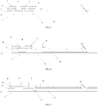
- FIG. 3 is a cross-sectional view at a third electrode of a substrate of a touch display screen pr ovided in an embodiment of the present invention
- FIG. 4 is a cross-sectional view at a second electrode of a substrate of a touch display screen provided in an embodiment of the pr esent invention
- FIG. 5 is a cross-sectional view at a first electrode of a substrate of a touch display screen provided in an embodiment of the present invention.
- a TFT substrate is provided, an ITO layer is deposited on a surface of the TFT substrate, and is patterned by using lithography technology to form second electrodes 12 (common elect rode Vcom), fourth electrodes 14 (common electrode/touch receiv ing electrode Vcom/Rx) and first electrodes 11 (common electrode/touch transmitting electrode Vcom/Tx).
- second electrodes 12 common elect rode Vcom
- fourth electrodes 14 common electrode/touch receiv ing electrode Vcom/Rx
- first electrodes 11 common electrode/touch transmitting electrode Vcom/Tx
- a metal layer is deposited thereon, and is patterned by using lithography technology to form a gate 2 (Gate), and a connecting line 9 (Tx), which is connected to the previously-formed third electrodes 11 (Vcom/Tx) and spaced apart from the second electrodes (Vcom) and th e fourth electrodes 14 (Vcom/Rx) by a certain gap.
- Gate gate 2
- Tx connecting line 9
- a gate insulation layer 3 (GI) is deposited on the formed gate 2.
- a semiconductor layer i.e., an active layer 4
- an active layer 4 which may include an amorphous silicon layer (Active) and a light ly doped amorphous silicon layer (n+)
- a second metal layer SD
- the semiconductor layer and the second metal layer are patterned by lithography technology to form a thin film transistor channel, a source 5 (S), a drain 7 (D), and a data line (D).
- a protection layer 6 is deposit ed thereon, and is patterned by using lithography technology to form a connecting hole for a pixel electrode 8, a connecting hole for the touch transmitting electrode, a connecting hole for the touch receiving electrode and a connecting hole for the common electrode.
- an ITO layer is deposited th ereon, and the pixel electrode 8 and the electrode connecting layer 13 are patterned by using lithography technology.
- An embodiment of the present invention further provides a t ouch screen, which includes any one of the substrates described above.
- electrodes are provided on the base substrate, and particularly, among the electrodes, the fourth electrodes 14 serve as the common electrode and the touch receiving electrode, the third electrodes 11 serve as the common electrode and the touch transmitting electrode , coupling capacitors are formed by means of the connecting lines 9 and the electrode connecting layer 13, and the fourth electrodes 14 and the third electrodes 11 are driven in a time division manner.
- the touch receiving electrode and the touch transmitting electrode may be provided in a same layer.
- the touch transmitting elec trode and the touch receiving electrode may be formed on the formed common electrode. In this way, the structure of the substrate is simplified, the production provics of the substrate are reduced, and fabrication costs of the substrate are lowered.
- An embodiment of the present invention further provides a display device, which includes the touch screen described above.
- electrodes are provided on the base substrate, particularly, among the electrodes, the fourth electrode s 14 serve as the common electrode and the touch receiving electrode, the third electrodes 11 serve as the common electrode and th e touch transmitting electrode , coupling capacitors are formed by means of the connecting lines 9 and the electrode connecting layer 13, and the fourth electrodes 14 a nd the third electrodes 11 are driven in a time division manner.
- the touch receiving electrode and the touch transmitting electrode may be provided in a same layer.
- the touch transmitting elec trode and the touch receiving electrode may be formed on the formed common electrode.
- the structure of the substrate is simplified, the production processes of the substrate are reduced, and fabrication costs of the substrate are lowered.
- capacitance of the coupling capacitor formed between the electrode connecting layer 13 and the touch receiving el ectrode is affected, thus the capacitance of the coupling capacitor at the touch position of the operator becomes different from that of the coupling capacitor at other position, and the touch screen determines the touch position of the operator based on the received position of the coupling capacitor with changed capacitance.
Landscapes
- Physics & Mathematics (AREA)
- Engineering & Computer Science (AREA)
- Theoretical Computer Science (AREA)
- General Engineering & Computer Science (AREA)
- General Physics & Mathematics (AREA)
- Nonlinear Science (AREA)
- Human Computer Interaction (AREA)
- Mathematical Physics (AREA)
- Optics & Photonics (AREA)
- Crystallography & Structural Chemistry (AREA)
- Chemical & Material Sciences (AREA)
- Microelectronics & Electronic Packaging (AREA)
- Geometry (AREA)
- Devices For Indicating Variable Information By Combining Individual Elements (AREA)
- Position Input By Displaying (AREA)
Applications Claiming Priority (2)
| Application Number | Priority Date | Filing Date | Title |
|---|---|---|---|
| CN201410855010.3A CN104503647B (zh) | 2014-12-31 | 2014-12-31 | 一种触摸显示屏的基板及其制造方法、触摸屏及显示装置 |
| PCT/CN2015/094752 WO2016107310A1 (fr) | 2014-12-31 | 2015-11-17 | Substrat d'écran d'affichage tactile et son procédé de fabrication, écran tactile et dispositif d'affichage |
Publications (3)
| Publication Number | Publication Date |
|---|---|
| EP3242191A1 true EP3242191A1 (fr) | 2017-11-08 |
| EP3242191A4 EP3242191A4 (fr) | 2018-08-01 |
| EP3242191B1 EP3242191B1 (fr) | 2020-05-27 |
Family
ID=52945048
Family Applications (1)
| Application Number | Title | Priority Date | Filing Date |
|---|---|---|---|
| EP15874991.1A Active EP3242191B1 (fr) | 2014-12-31 | 2015-11-17 | Substrat d'écran d'affichage tactile et son procédé de fabrication, écran tactile et dispositif d'affichage |
Country Status (4)
| Country | Link |
|---|---|
| US (1) | US9927647B2 (fr) |
| EP (1) | EP3242191B1 (fr) |
| CN (1) | CN104503647B (fr) |
| WO (1) | WO2016107310A1 (fr) |
Families Citing this family (5)
| Publication number | Priority date | Publication date | Assignee | Title |
|---|---|---|---|---|
| CN104503647B (zh) | 2014-12-31 | 2017-12-08 | 京东方科技集团股份有限公司 | 一种触摸显示屏的基板及其制造方法、触摸屏及显示装置 |
| CN104915054B (zh) | 2015-05-14 | 2019-10-15 | 京东方科技集团股份有限公司 | 阵列基板及其制作方法和显示装置 |
| US10684500B2 (en) | 2015-05-27 | 2020-06-16 | Semiconductor Energy Laboratory Co., Ltd. | Touch panel |
| CN105629545A (zh) * | 2016-01-19 | 2016-06-01 | 深圳市华星光电技术有限公司 | 触摸面板以及其制造方法 |
| CN110187787A (zh) * | 2018-02-22 | 2019-08-30 | 蓝思科技(长沙)有限公司 | 一种触控屏边框 |
Family Cites Families (23)
| Publication number | Priority date | Publication date | Assignee | Title |
|---|---|---|---|---|
| KR101284714B1 (ko) * | 2010-09-20 | 2013-07-17 | 엘지디스플레이 주식회사 | 액정 표시장치와 이의 제조방법 |
| KR101273239B1 (ko) * | 2010-09-20 | 2013-06-11 | 엘지디스플레이 주식회사 | 터치 스크린이 내장된 액정 표시장치와 이의 제조방법 |
| CN103135815B (zh) * | 2011-11-25 | 2017-02-22 | 上海天马微电子有限公司 | 内嵌触摸屏液晶显示装置及其触控驱动方法 |
| KR101353284B1 (ko) * | 2012-04-25 | 2014-01-21 | 엘지디스플레이 주식회사 | 액정 디스플레이 장치와 이의 제조방법 |
| TWI464643B (zh) * | 2012-05-25 | 2014-12-11 | J Touch Corp | 偏光片之觸控感應元件製作方法與偏光裝置 |
| CN102841717B (zh) * | 2012-08-31 | 2015-04-01 | 北京京东方光电科技有限公司 | 一种电容式触摸屏及其制造方法 |
| CN103092452B (zh) * | 2013-01-28 | 2016-03-23 | 北京京东方光电科技有限公司 | 电容触摸屏及其制作方法和触摸显示装置 |
| CN103150070B (zh) * | 2013-03-05 | 2016-07-06 | 合肥京东方光电科技有限公司 | 一种电容式触控模组、电容式内嵌触摸屏及显示装置 |
| CN203117953U (zh) * | 2013-03-05 | 2013-08-07 | 合肥京东方光电科技有限公司 | 一种电容式触控模组、电容式内嵌触摸屏及显示装置 |
| KR102078831B1 (ko) | 2013-03-12 | 2020-04-03 | 삼성디스플레이 주식회사 | 플렉서블 터치 스크린 패널을 구비한 플렉서블 표시장치 |
| CN104216578A (zh) * | 2013-05-30 | 2014-12-17 | 京东方科技集团股份有限公司 | 一种触摸面板及显示装置 |
| CN203376696U (zh) * | 2013-06-06 | 2014-01-01 | 敦泰科技有限公司 | 触控显示装置 |
| KR102092569B1 (ko) * | 2013-09-17 | 2020-03-25 | 엘지디스플레이 주식회사 | 터치 스크린 일체형 디스플레이 장치와 이의 구동 방법 |
| CN103699284B (zh) * | 2013-12-27 | 2016-09-21 | 京东方科技集团股份有限公司 | 一种电容式内嵌触摸屏及其制备方法、显示装置 |
| CN103885637B (zh) * | 2014-03-12 | 2017-05-31 | 京东方科技集团股份有限公司 | 一种内嵌式触摸屏及显示装置 |
| CN103955320B (zh) * | 2014-04-21 | 2017-02-15 | 合肥鑫晟光电科技有限公司 | 触摸基板及触摸屏 |
| CN104035640B (zh) * | 2014-05-30 | 2017-10-27 | 京东方科技集团股份有限公司 | 一种内嵌式触摸屏及显示装置 |
| CN104020891A (zh) * | 2014-05-30 | 2014-09-03 | 京东方科技集团股份有限公司 | 一种内嵌式触摸屏及显示装置 |
| CN104199580A (zh) | 2014-08-29 | 2014-12-10 | 合肥鑫晟光电科技有限公司 | 一种触摸屏、其制作方法及触摸显示装置 |
| CN104216564B (zh) * | 2014-09-01 | 2017-09-01 | 上海天马微电子有限公司 | 一种触摸屏、触摸显示面板及显示装置 |
| CN104238854B (zh) * | 2014-09-10 | 2018-01-02 | 京东方科技集团股份有限公司 | 一种阵列基板和具有该阵列基板的电容式内嵌触摸屏 |
| CN204515743U (zh) * | 2014-12-31 | 2015-07-29 | 京东方科技集团股份有限公司 | 一种触摸显示屏的基板、触摸屏及显示装置 |
| CN104503647B (zh) * | 2014-12-31 | 2017-12-08 | 京东方科技集团股份有限公司 | 一种触摸显示屏的基板及其制造方法、触摸屏及显示装置 |
-
2014
- 2014-12-31 CN CN201410855010.3A patent/CN104503647B/zh active Active
-
2015
- 2015-11-17 US US15/325,146 patent/US9927647B2/en active Active
- 2015-11-17 WO PCT/CN2015/094752 patent/WO2016107310A1/fr not_active Ceased
- 2015-11-17 EP EP15874991.1A patent/EP3242191B1/fr active Active
Also Published As
| Publication number | Publication date |
|---|---|
| EP3242191B1 (fr) | 2020-05-27 |
| CN104503647A (zh) | 2015-04-08 |
| WO2016107310A1 (fr) | 2016-07-07 |
| US20170184896A1 (en) | 2017-06-29 |
| US9927647B2 (en) | 2018-03-27 |
| EP3242191A4 (fr) | 2018-08-01 |
| CN104503647B (zh) | 2017-12-08 |
Similar Documents
| Publication | Publication Date | Title |
|---|---|---|
| US9927911B2 (en) | Touch display panel and fabrication method thereof, and touch display apparatus | |
| KR101470607B1 (ko) | 컬러 필터 기판 및 용량성 터치 스크린 | |
| CN104597670B (zh) | 一种阵列基板及其制作方法及显示装置 | |
| US10067613B2 (en) | Touch display device | |
| US9310948B2 (en) | Array substrate, touch screen panel and display device | |
| CN104536636B (zh) | 一种阵列基板、触控面板及阵列基板的制作方法 | |
| US9990090B2 (en) | Touch display device | |
| TWI492115B (zh) | 內嵌式觸控面板 | |
| US10303297B2 (en) | Touch display panel and driving method therefor, and display device | |
| US9224762B1 (en) | Array substrate and display device | |
| CN104571715A (zh) | 阵列基板及其制作方法和驱动方法、显示装置 | |
| WO2017197934A1 (fr) | Substrat de réseau et son procédé de fabrication, ainsi qu'un appareil d'affichage tactile | |
| EP3242191A1 (fr) | Substrat d'écran d'affichage tactile et son procédé de fabrication, écran tactile et dispositif d'affichage | |
| WO2015161612A1 (fr) | Substrat et écran tactiles | |
| WO2016123932A1 (fr) | Substrat de film coloré et dispositif d'affichage | |
| US20200319739A1 (en) | Touch display panel | |
| WO2014153809A1 (fr) | Écran tactile capacitif intégré et appareil d'affichage | |
| US20170269746A1 (en) | In-cell touch screen and display device | |
| WO2015180288A1 (fr) | Ecran tactile intégré et dispositif d'affichage | |
| CN107678590B (zh) | 一种触控显示面板及其驱动方法 | |
| US20160048239A1 (en) | Array substrate and manufacturing method thereof, touch display device | |
| WO2018014679A1 (fr) | Substrat tactile, appareil d'affichage à commande tactile et procédé de fabrication | |
| US20160162072A1 (en) | Touch panel, manufacturing method thereof and display device | |
| US10001853B2 (en) | Touch grating cell and touch stereoscopic display device | |
| US20160026288A1 (en) | Touch display panel, display device and method for manufacturing color filter substrate |
Legal Events
| Date | Code | Title | Description |
|---|---|---|---|
| STAA | Information on the status of an ep patent application or granted ep patent |
Free format text: STATUS: THE INTERNATIONAL PUBLICATION HAS BEEN MADE |
|
| PUAI | Public reference made under article 153(3) epc to a published international application that has entered the european phase |
Free format text: ORIGINAL CODE: 0009012 |
|
| STAA | Information on the status of an ep patent application or granted ep patent |
Free format text: STATUS: REQUEST FOR EXAMINATION WAS MADE |
|
| 17P | Request for examination filed |
Effective date: 20170111 |
|
| AK | Designated contracting states |
Kind code of ref document: A1 Designated state(s): AL AT BE BG CH CY CZ DE DK EE ES FI FR GB GR HR HU IE IS IT LI LT LU LV MC MK MT NL NO PL PT RO RS SE SI SK SM TR |
|
| AX | Request for extension of the european patent |
Extension state: BA ME |
|
| DAV | Request for validation of the european patent (deleted) | ||
| DAX | Request for extension of the european patent (deleted) | ||
| A4 | Supplementary search report drawn up and despatched |
Effective date: 20180703 |
|
| RIC1 | Information provided on ipc code assigned before grant |
Ipc: G06F 3/041 20060101ALI20180627BHEP Ipc: G06F 3/044 20060101AFI20180627BHEP |
|
| GRAP | Despatch of communication of intention to grant a patent |
Free format text: ORIGINAL CODE: EPIDOSNIGR1 |
|
| STAA | Information on the status of an ep patent application or granted ep patent |
Free format text: STATUS: GRANT OF PATENT IS INTENDED |
|
| RIC1 | Information provided on ipc code assigned before grant |
Ipc: G02F 1/1343 20060101ALI20200225BHEP Ipc: G06F 3/041 20060101ALI20200225BHEP Ipc: G02F 1/1333 20060101ALI20200225BHEP Ipc: G06F 3/044 20060101AFI20200225BHEP |
|
| INTG | Intention to grant announced |
Effective date: 20200320 |
|
| GRAS | Grant fee paid |
Free format text: ORIGINAL CODE: EPIDOSNIGR3 |
|
| GRAA | (expected) grant |
Free format text: ORIGINAL CODE: 0009210 |
|
| STAA | Information on the status of an ep patent application or granted ep patent |
Free format text: STATUS: THE PATENT HAS BEEN GRANTED |
|
| AK | Designated contracting states |
Kind code of ref document: B1 Designated state(s): AL AT BE BG CH CY CZ DE DK EE ES FI FR GB GR HR HU IE IS IT LI LT LU LV MC MK MT NL NO PL PT RO RS SE SI SK SM TR |
|
| REG | Reference to a national code |
Ref country code: GB Ref legal event code: FG4D |
|
| REG | Reference to a national code |
Ref country code: CH Ref legal event code: EP |
|
| REG | Reference to a national code |
Ref country code: DE Ref legal event code: R096 Ref document number: 602015053583 Country of ref document: DE |
|
| REG | Reference to a national code |
Ref country code: AT Ref legal event code: REF Ref document number: 1275234 Country of ref document: AT Kind code of ref document: T Effective date: 20200615 |
|
| REG | Reference to a national code |
Ref country code: LT Ref legal event code: MG4D |
|
| PG25 | Lapsed in a contracting state [announced via postgrant information from national office to epo] |
Ref country code: LT Free format text: LAPSE BECAUSE OF FAILURE TO SUBMIT A TRANSLATION OF THE DESCRIPTION OR TO PAY THE FEE WITHIN THE PRESCRIBED TIME-LIMIT Effective date: 20200527 Ref country code: NO Free format text: LAPSE BECAUSE OF FAILURE TO SUBMIT A TRANSLATION OF THE DESCRIPTION OR TO PAY THE FEE WITHIN THE PRESCRIBED TIME-LIMIT Effective date: 20200827 Ref country code: FI Free format text: LAPSE BECAUSE OF FAILURE TO SUBMIT A TRANSLATION OF THE DESCRIPTION OR TO PAY THE FEE WITHIN THE PRESCRIBED TIME-LIMIT Effective date: 20200527 Ref country code: PT Free format text: LAPSE BECAUSE OF FAILURE TO SUBMIT A TRANSLATION OF THE DESCRIPTION OR TO PAY THE FEE WITHIN THE PRESCRIBED TIME-LIMIT Effective date: 20200928 Ref country code: SE Free format text: LAPSE BECAUSE OF FAILURE TO SUBMIT A TRANSLATION OF THE DESCRIPTION OR TO PAY THE FEE WITHIN THE PRESCRIBED TIME-LIMIT Effective date: 20200527 Ref country code: IS Free format text: LAPSE BECAUSE OF FAILURE TO SUBMIT A TRANSLATION OF THE DESCRIPTION OR TO PAY THE FEE WITHIN THE PRESCRIBED TIME-LIMIT Effective date: 20200927 Ref country code: GR Free format text: LAPSE BECAUSE OF FAILURE TO SUBMIT A TRANSLATION OF THE DESCRIPTION OR TO PAY THE FEE WITHIN THE PRESCRIBED TIME-LIMIT Effective date: 20200828 |
|
| REG | Reference to a national code |
Ref country code: NL Ref legal event code: MP Effective date: 20200527 |
|
| PG25 | Lapsed in a contracting state [announced via postgrant information from national office to epo] |
Ref country code: HR Free format text: LAPSE BECAUSE OF FAILURE TO SUBMIT A TRANSLATION OF THE DESCRIPTION OR TO PAY THE FEE WITHIN THE PRESCRIBED TIME-LIMIT Effective date: 20200527 Ref country code: RS Free format text: LAPSE BECAUSE OF FAILURE TO SUBMIT A TRANSLATION OF THE DESCRIPTION OR TO PAY THE FEE WITHIN THE PRESCRIBED TIME-LIMIT Effective date: 20200527 Ref country code: BG Free format text: LAPSE BECAUSE OF FAILURE TO SUBMIT A TRANSLATION OF THE DESCRIPTION OR TO PAY THE FEE WITHIN THE PRESCRIBED TIME-LIMIT Effective date: 20200827 Ref country code: LV Free format text: LAPSE BECAUSE OF FAILURE TO SUBMIT A TRANSLATION OF THE DESCRIPTION OR TO PAY THE FEE WITHIN THE PRESCRIBED TIME-LIMIT Effective date: 20200527 |
|
| REG | Reference to a national code |
Ref country code: AT Ref legal event code: MK05 Ref document number: 1275234 Country of ref document: AT Kind code of ref document: T Effective date: 20200527 |
|
| PG25 | Lapsed in a contracting state [announced via postgrant information from national office to epo] |
Ref country code: AL Free format text: LAPSE BECAUSE OF FAILURE TO SUBMIT A TRANSLATION OF THE DESCRIPTION OR TO PAY THE FEE WITHIN THE PRESCRIBED TIME-LIMIT Effective date: 20200527 Ref country code: NL Free format text: LAPSE BECAUSE OF FAILURE TO SUBMIT A TRANSLATION OF THE DESCRIPTION OR TO PAY THE FEE WITHIN THE PRESCRIBED TIME-LIMIT Effective date: 20200527 |
|
| PG25 | Lapsed in a contracting state [announced via postgrant information from national office to epo] |
Ref country code: ES Free format text: LAPSE BECAUSE OF FAILURE TO SUBMIT A TRANSLATION OF THE DESCRIPTION OR TO PAY THE FEE WITHIN THE PRESCRIBED TIME-LIMIT Effective date: 20200527 Ref country code: CZ Free format text: LAPSE BECAUSE OF FAILURE TO SUBMIT A TRANSLATION OF THE DESCRIPTION OR TO PAY THE FEE WITHIN THE PRESCRIBED TIME-LIMIT Effective date: 20200527 Ref country code: RO Free format text: LAPSE BECAUSE OF FAILURE TO SUBMIT A TRANSLATION OF THE DESCRIPTION OR TO PAY THE FEE WITHIN THE PRESCRIBED TIME-LIMIT Effective date: 20200527 Ref country code: IT Free format text: LAPSE BECAUSE OF FAILURE TO SUBMIT A TRANSLATION OF THE DESCRIPTION OR TO PAY THE FEE WITHIN THE PRESCRIBED TIME-LIMIT Effective date: 20200527 Ref country code: DK Free format text: LAPSE BECAUSE OF FAILURE TO SUBMIT A TRANSLATION OF THE DESCRIPTION OR TO PAY THE FEE WITHIN THE PRESCRIBED TIME-LIMIT Effective date: 20200527 Ref country code: AT Free format text: LAPSE BECAUSE OF FAILURE TO SUBMIT A TRANSLATION OF THE DESCRIPTION OR TO PAY THE FEE WITHIN THE PRESCRIBED TIME-LIMIT Effective date: 20200527 Ref country code: EE Free format text: LAPSE BECAUSE OF FAILURE TO SUBMIT A TRANSLATION OF THE DESCRIPTION OR TO PAY THE FEE WITHIN THE PRESCRIBED TIME-LIMIT Effective date: 20200527 Ref country code: SM Free format text: LAPSE BECAUSE OF FAILURE TO SUBMIT A TRANSLATION OF THE DESCRIPTION OR TO PAY THE FEE WITHIN THE PRESCRIBED TIME-LIMIT Effective date: 20200527 |
|
| PG25 | Lapsed in a contracting state [announced via postgrant information from national office to epo] |
Ref country code: SK Free format text: LAPSE BECAUSE OF FAILURE TO SUBMIT A TRANSLATION OF THE DESCRIPTION OR TO PAY THE FEE WITHIN THE PRESCRIBED TIME-LIMIT Effective date: 20200527 Ref country code: PL Free format text: LAPSE BECAUSE OF FAILURE TO SUBMIT A TRANSLATION OF THE DESCRIPTION OR TO PAY THE FEE WITHIN THE PRESCRIBED TIME-LIMIT Effective date: 20200527 |
|
| REG | Reference to a national code |
Ref country code: DE Ref legal event code: R097 Ref document number: 602015053583 Country of ref document: DE |
|
| PLBE | No opposition filed within time limit |
Free format text: ORIGINAL CODE: 0009261 |
|
| STAA | Information on the status of an ep patent application or granted ep patent |
Free format text: STATUS: NO OPPOSITION FILED WITHIN TIME LIMIT |
|
| 26N | No opposition filed |
Effective date: 20210302 |
|
| PG25 | Lapsed in a contracting state [announced via postgrant information from national office to epo] |
Ref country code: SI Free format text: LAPSE BECAUSE OF FAILURE TO SUBMIT A TRANSLATION OF THE DESCRIPTION OR TO PAY THE FEE WITHIN THE PRESCRIBED TIME-LIMIT Effective date: 20200527 |
|
| PG25 | Lapsed in a contracting state [announced via postgrant information from national office to epo] |
Ref country code: MC Free format text: LAPSE BECAUSE OF FAILURE TO SUBMIT A TRANSLATION OF THE DESCRIPTION OR TO PAY THE FEE WITHIN THE PRESCRIBED TIME-LIMIT Effective date: 20200527 |
|
| REG | Reference to a national code |
Ref country code: CH Ref legal event code: PL |
|
| PG25 | Lapsed in a contracting state [announced via postgrant information from national office to epo] |
Ref country code: LU Free format text: LAPSE BECAUSE OF NON-PAYMENT OF DUE FEES Effective date: 20201117 |
|
| REG | Reference to a national code |
Ref country code: BE Ref legal event code: MM Effective date: 20201130 |
|
| PG25 | Lapsed in a contracting state [announced via postgrant information from national office to epo] |
Ref country code: CH Free format text: LAPSE BECAUSE OF NON-PAYMENT OF DUE FEES Effective date: 20201130 Ref country code: LI Free format text: LAPSE BECAUSE OF NON-PAYMENT OF DUE FEES Effective date: 20201130 |
|
| PG25 | Lapsed in a contracting state [announced via postgrant information from national office to epo] |
Ref country code: IE Free format text: LAPSE BECAUSE OF NON-PAYMENT OF DUE FEES Effective date: 20201117 Ref country code: FR Free format text: LAPSE BECAUSE OF NON-PAYMENT OF DUE FEES Effective date: 20201130 |
|
| PG25 | Lapsed in a contracting state [announced via postgrant information from national office to epo] |
Ref country code: TR Free format text: LAPSE BECAUSE OF FAILURE TO SUBMIT A TRANSLATION OF THE DESCRIPTION OR TO PAY THE FEE WITHIN THE PRESCRIBED TIME-LIMIT Effective date: 20200527 Ref country code: MT Free format text: LAPSE BECAUSE OF FAILURE TO SUBMIT A TRANSLATION OF THE DESCRIPTION OR TO PAY THE FEE WITHIN THE PRESCRIBED TIME-LIMIT Effective date: 20200527 Ref country code: CY Free format text: LAPSE BECAUSE OF FAILURE TO SUBMIT A TRANSLATION OF THE DESCRIPTION OR TO PAY THE FEE WITHIN THE PRESCRIBED TIME-LIMIT Effective date: 20200527 |
|
| PG25 | Lapsed in a contracting state [announced via postgrant information from national office to epo] |
Ref country code: MK Free format text: LAPSE BECAUSE OF FAILURE TO SUBMIT A TRANSLATION OF THE DESCRIPTION OR TO PAY THE FEE WITHIN THE PRESCRIBED TIME-LIMIT Effective date: 20200527 |
|
| PG25 | Lapsed in a contracting state [announced via postgrant information from national office to epo] |
Ref country code: BE Free format text: LAPSE BECAUSE OF NON-PAYMENT OF DUE FEES Effective date: 20201130 |
|
| PGFP | Annual fee paid to national office [announced via postgrant information from national office to epo] |
Ref country code: DE Payment date: 20251121 Year of fee payment: 11 |
|
| PGFP | Annual fee paid to national office [announced via postgrant information from national office to epo] |
Ref country code: GB Payment date: 20251121 Year of fee payment: 11 |