EP3244345B1 - Procédé de reconnaissance d'image, dispositif terminal et accélérateur de reconnaissance d'image - Google Patents
Procédé de reconnaissance d'image, dispositif terminal et accélérateur de reconnaissance d'image Download PDFInfo
- Publication number
- EP3244345B1 EP3244345B1 EP16761030.2A EP16761030A EP3244345B1 EP 3244345 B1 EP3244345 B1 EP 3244345B1 EP 16761030 A EP16761030 A EP 16761030A EP 3244345 B1 EP3244345 B1 EP 3244345B1
- Authority
- EP
- European Patent Office
- Prior art keywords
- image recognition
- dimensionality
- adjusted
- success rate
- parameter
- Prior art date
- Legal status (The legal status is an assumption and is not a legal conclusion. Google has not performed a legal analysis and makes no representation as to the accuracy of the status listed.)
- Active
Links
Images


Classifications
-
- G—PHYSICS
- G06—COMPUTING OR CALCULATING; COUNTING
- G06V—IMAGE OR VIDEO RECOGNITION OR UNDERSTANDING
- G06V10/00—Arrangements for image or video recognition or understanding
- G06V10/20—Image preprocessing
-
- G—PHYSICS
- G06—COMPUTING OR CALCULATING; COUNTING
- G06V—IMAGE OR VIDEO RECOGNITION OR UNDERSTANDING
- G06V10/00—Arrangements for image or video recognition or understanding
- G06V10/94—Hardware or software architectures specially adapted for image or video understanding
-
- G—PHYSICS
- G06—COMPUTING OR CALCULATING; COUNTING
- G06F—ELECTRIC DIGITAL DATA PROCESSING
- G06F18/00—Pattern recognition
- G06F18/20—Analysing
- G06F18/22—Matching criteria, e.g. proximity measures
-
- G—PHYSICS
- G06—COMPUTING OR CALCULATING; COUNTING
- G06T—IMAGE DATA PROCESSING OR GENERATION, IN GENERAL
- G06T1/00—General purpose image data processing
- G06T1/20—Processor architectures; Processor configuration, e.g. pipelining
Definitions
- the present invention relates to the field of computer technologies, and in particular, to an image recognition accelerator, a terminal device, and an image recognition method.
- Image recognition technologies are an important field of artificial intelligence.
- Image recognition refers to a technology that uses a computer to process and analyze an image, to recognize different targets and objects.
- image recognition refers to a technology that uses a computer to process and analyze an image, to recognize different targets and objects.
- image data analysis In recent years, with the popularity of social networks, there are increasing demands for real-time image data analysis on a mobile device. However, because a relatively large quantity of system resources are consumed for implementation of image data analysis, a limited battery lifespan of a mobile device restricts application of image data analysis to mobile devices.
- an image data processing method in the prior art reduces the system power consumption in a manner of lowering a write current that is used to write image data into a static random-access memory (Static Random-Access Memory, SRAM).
- SRAM static random-access memory
- an error rate of data stored in the SRAM increases as the write current is lowered.
- a manner such as convex optimization (convex optimization) processing is further required to recover the stored image data, so that image recognition can be performed based on the recovered image data.
- convex optimization convex optimization
- the SRAM In addition, to protect the data stored in the SRAM, the SRAM needs to stay in a power-on state. Therefore, the SRAM also has a static power consumption. In the foregoing image data processing manner, the static power consumption that is required for the SRAM to protect the data still cannot be eliminated. As a result, generally, when the existing image data processing manner is used to process image data, a system power consumption is still relatively high.
- the present invention provides an image recognition accelerator, a terminal device, and an image recognition method, which can ensure accuracy of image recognition while reducing a system power consumption of the terminal device.
- the present invention provides an image recognition accelerator applied to a terminal device for image recognition, including: a dimensionality-reduction processing module, configured to reduce a dimensionality of first image data according to a specified dimensionality-reduction parameter ⁇ , where the first image data on which dimensionality reduction has been performed includes multiple numeric values; a non-volatile memory NVM, configured to: store, in a first storage area of the NVM according to a specified first current I, ⁇ low-order bits of each numeric value of the first image data on which dimensionality reduction has been performed, and store, in a second storage area of the NVM according to a specified second current I s , (N- ⁇ ) high-order bits of each numeric value of the first image data on which dimensionality reduction has been performed, where N is a quantity of bits occupied by each numeric value, ⁇ is a specified width parameter, the first current I is lower than the second current I s , and the dimensionality-reduction parameter ⁇ , the width parameter
- the image recognition accelerator further includes a parameter adjustment module, configured to: if an absolute value of a difference between a calculated image recognition success rate and a specified second image recognition success rate is greater than a preset threshold, adjust, according to the second image recognition success rate and the system power consumption of the terminal device, at least one of the following parameters: the dimensionality-reduction parameter, the width parameter, or the first current, to obtain an adjusted dimensionality-reduction parameter ⁇ ', an adjusted width parameter ⁇ ', and an adjusted first current I', where the second image recognition success rate is different from the first image recognition success rate; the dimensionality-reduction processing module is further configured to reduce a dimensionality of second image data according to the adjusted dimensionality-reduction parameter ⁇ '; the non-volatile memory NVM is further configured to store, in the first storage area of the NVM according to the adjusted first current I', ⁇ ' low-order bits of each numeric value of the second image data on which dimensional
- the parameter adjustment module is specifically configured to:
- the present invention provides a terminal device, where the terminal device includes a CPU and an image recognition accelerator; the CPU is configured to send to-be-recognized first image data to the image recognition accelerator; and the image recognition accelerator is configured to: reduce a dimensionality of the first image data according to a specified dimensionality-reduction parameter ⁇ , where the first image data on which dimensionality reduction has been performed includes multiple numeric values; store, in a first storage area of an NVM according to a specified first current I, ⁇ low-order bits of each numeric value of the first image data on which dimensionality reduction has been performed, and store, in a second storage area of the NVM according to a specified second current I s , (N-co) high-order bits of each numeric value of the first image data on which dimensionality reduction has been performed, where N is a quantity of bits occupied by each numeric value, ⁇ is a specified width parameter, I is lower than I s , and the dimensionality-reduction parameter ⁇
- the image recognition accelerator is further configured to: if an absolute value of a difference between a calculated image recognition success rate and a specified second image recognition success rate is greater than a preset threshold, adjust, according to the second image recognition success rate and the system power consumption of the terminal device, a value of at least one of the following parameters: the dimensionality-reduction parameter, the width parameter, or the first current, to obtain an adjusted dimensionality-reduction parameter y', an adjusted width parameter ⁇ ', and an adjusted first current I', where the second image recognition success rate is different from the first image recognition success rate; the CPU is further configured to send second image data to the image recognition accelerator; and the image recognition accelerator is further configured to:
- the CPU is further configured to: collect statistics on matching results that are output by the image recognition accelerator within a preset statistic collection period, to obtain a calculated image recognition success rate; and determine that an absolute value of a difference between the calculated image recognition success rate and a specified second image recognition success rate is greater than a preset threshold; the image recognition accelerator is further configured to adjust, according to the second image recognition success rate and the system power consumption of the terminal device, at least one of the following parameters: the dimensionality-reduction parameter, the width parameter, or the first current, to obtain an adjusted dimensionality-reduction parameter ⁇ ', an adjusted width parameter ⁇ ', and an adjusted first current I', where the second image recognition success rate is different from the first image recognition success rate; the CPU is further configured to send second image data to the image recognition accelerator; and the image recognition accelerator is further configured to: reduce a dimensionality of the second image data according to the adjusted dimensionality-reduction parameter ⁇ '; store, in the first storage area of
- the CPU is further configured to:
- the image recognition accelerator is specifically configured to:
- the CPU is specifically configured to:
- the present invention provides an image recognition method applied to a terminal device, where the method is executed by an image recognition accelerator in the terminal device, and the method includes:
- the method further includes:
- the adjusting, according to the second image recognition success rate and the system power consumption of the terminal device, at least one of the following parameters: the dimensionality-reduction parameter, the width parameter, or the first current includes:
- the present invention provides a computer program product, including a computer readable storage medium that stores program code, where an instruction included in the program code is used to execute the method in the foregoing third aspect.
- the present invention provides another image recognition accelerator applied to a terminal device for image recognition.
- the image recognition accelerator includes a dimensionality-reduction processing module, a non-volatile memory NVM, and an image matching module.
- the dimensionality-reduction processing module is configured to: receive a dimensionality-reduction parameter ⁇ , and reduce a dimensionality of first image data according to the received dimensionality-reduction parameter ⁇ , where the first image data on which dimensionality reduction has been performed includes multiple numeric values, and the dimensionality-reduction parameter ⁇ is obtained according to a system power consumption of the terminal device and a specified first image recognition success rate of the terminal device.
- the non-volatile memory NVM is configured to: receive a width parameter ⁇ and a first current I, obtain a storage bit quantity S according to the received width parameter ⁇ , store, in a first storage area of the NVM according to the specified first current I, S low-order bits of each numeric value of the first image data on which dimensionality reduction has been performed, and store, in a second storage area of the NVM according to a specified second current I s , (N-S) high-order bits of each numeric value of the first image data on which dimensionality reduction has been performed, where N is a quantity of bits occupied by each numeric value, the first current I is lower than the second current I s , and the width parameter ⁇ and the first current I are obtained according to the system power consumption of the terminal device and the specified first image recognition success rate of the terminal device.
- the image matching module is configured to determine whether an image library stored in the NVM includes image data matching the first image data on which dimensionality reduction has been performed.
- the image recognition accelerator further includes a parameter adjustment module.
- the parameter adjustment module is configured to: adjust, according to the specified first image recognition success rate and the system power consumption of the terminal device, a value of at least one of the following parameters: the dimensionality-reduction parameter, the width parameter, or the first current, to obtain the dimensionality-reduction parameter ⁇ , the width parameter ⁇ , or the first current I; send the dimensionality-reduction parameter ⁇ to the dimensionality-reduction processing module; and send the width parameter ⁇ and the first current I to the NVM.
- the parameter adjustment module is specifically configured to: separately adjust the value of the dimensionality-reduction parameter, the width parameter, or the first current, and separately obtain multiple adjusted image recognition success rates and multiple adjusted system power consumptions, where each adjusted image recognition success rate is corresponding to one adjusted system power consumption; determine a difference between each adjusted image recognition success rate and the first image recognition success rate, and select a lowest system power consumption from at least one adjusted system power consumption corresponding to at least one adjusted image recognition success rate, where an absolute value of a difference between the at least one adjusted image recognition success rate and the first image recognition success rate is not greater than a preset threshold; select values of the dimensionality-reduction parameter, the width parameter, and the first current that make a highest image recognition success rate while satisfying the lowest system power consumption, as the dimensionality-reduction parameter ⁇ , the width parameter ⁇ , and the first current I, respectively; send the dimensionality-reduction parameter ⁇ to the dimensionality-reduction processing module; and send the width
- an image recognition accelerator applied to a terminal device for image recognition includes a dimensionality-reduction processing module, an NVM, and an image matching module.
- the dimensionality-reduction processing module first reduces a dimensionality of the first image data according to a specified dimensionality-reduction parameter ⁇ .
- the NVM may write, into a first storage area of the NVM according to a specified first current I, ⁇ low-order bits of each numeric value of the first image data on which dimensionality reduction has been performed, and write, into a second storage area of the NVM according to a specified second current I s , (N- ⁇ ) high-order bits of each numeric value of the first image data on which dimensionality reduction has been performed.
- the first current is lower than the second current.
- the image matching module may determine whether an image library stored in the NVM includes image data matching the first image data on which dimensionality reduction has been performed, so as to obtain an image recognition result for the first image data.
- the specified dimensionality-reduction parameter ⁇ , the width parameter ⁇ , and the first current I are all obtained according to a system power consumption of the terminal device and a specified first image recognition success rate of the terminal device; therefore, it can be ensured that an error that occurs in a storing process of low-order bits of a numeric value that are to be stored in the first storage area has relatively little impact on a recognition success rate for the first image data.
- the image recognition accelerator according to the present invention can ensure accuracy of image recognition while reducing the system power consumption of the terminal device, and can increase a speed of recognizing image data.
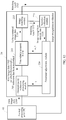
- FIG. 1 is a schematic structural diagram of a terminal device according to an embodiment of the present invention.
- a central processing unit (Central Processing Unit, CPU) 10 exchanges data directly with an image recognition accelerator 20 by using a bus 15.
- the bus 15 may be a system bus such as a PCI, a PCIE, or an accelerated graphics port AGP bus, and a type of the bus 15 is not limited in this embodiment of the present invention.
- the terminal device 100 shown in FIG. 1 may be a terminal device such as a computer, a mobile phone, or a mobile terminal, which is not limited herein provided that the terminal device is a terminal device requiring implementation of image recognition.
- the CPU 10 is a computing core (Core) and a control core (Control Unit) of the terminal device 100.
- the CPU 10 may be a very large scale integrated circuit.
- An operating system and another software program are installed on the CPU 10, which enable the CPU 10 to access storage space such as a memory and a cache.
- the CPU 10 is merely an example of a processor in this embodiment of the present invention.
- the processor may alternatively be another application-specific integrated circuit (Application Specific Integrated Circuit, ASIC), or one or more integrated circuits configured to implement this embodiment of the present invention.
- ASIC Application Specific Integrated Circuit
- the image recognition accelerator 20 is one type of hardware accelerator (hardware accelerator).
- the image recognition accelerator 20 is a hardware accelerator based on a non-volatile memory (Non-Volatile Memory, NVM).
- NVM Non-Volatile Memory
- a hardware acceleration technology uses a hardware module to substitute for a software algorithm, so as to fully utilize an inherent high-speed feature of hardware to increase a processing speed of a computer system.
- a memory is used only to store image data, while all processing and analysis of the image data is completed by a CPU; therefore, a processing speed of the CPU and transmission bandwidth of the memory have become bottlenecks for development of an image recognition technology.
- a simple logic processing circuit is added to the memory, so that a dedicated image recognition accelerator is used to implement image data processing.
- the CPU 10 only needs to send to-be-recognized image data to the image recognition accelerator 20 and receive a recognition result obtained by the image recognition accelerator 20. In this way, load of the CPU 10 is reduced, and an image recognition speed of the terminal device is increased.
- a data volume transmitted between the CPU 10 and the image recognition accelerator 20 is reduced; therefore, a problem that an image recognition speed is limited by transmission bandwidth of the memory can be resolved.
- FIG. 2 is a schematic structural diagram of another terminal device according to an embodiment of the present invention.
- the terminal device 100 shown in FIG. 2 may include a CPU 10, an image recognition accelerator 20, and an image data collector 30.
- the CPU 10 and the image data collector 30 are both connected to the image recognition accelerator 20.
- the image data collector 30 is configured to: collect image data information, and send the collected image data information to the image recognition accelerator 20 for image recognition.
- a person skilled in the art may know that the image data collector 30 may collect images of people or objects, and no specific limitation is imposed on image information herein. After collecting image information, the image data collector 30 may convert the collected image information into image data.
- the image data collector 30 may include a component that has a photo shooting or video shooting function.
- the image data collector may be a camera on a mobile phone.
- the image recognition accelerator 20 is configured to: recognize the image data information sent by the image data collector 30 and stored image data information, and send a recognition result to the CPU 10. It may be understood that, for functions and implementation manners of the CPU 10 and the image recognition accelerator 20 that are shown in FIG. 2 , reference may be made to the descriptions in the FIG. 1 . Details are not described herein again.
- the foregoing merely describes two schematic structures of the terminal device 100 provided in the embodiments of the present invention, and two application scenarios of the image recognition accelerator 20.
- the image recognition accelerator 20 may receive image data information sent by the CPU 10 and perform image recognition, and then send an image recognition result to another component or device.
- the image recognition accelerator 20 may receive image data information sent by another component (for example, the image data collector 30 in FIG. 2 ), and feed back an image recognition result to the component.
- a component that communicates with the image recognition accelerator 20 is not limited herein. The following describes in detail a specific structure and an operation process of the image recognition accelerator 20 provided in the embodiments of the present invention.
- FIG. 3 is a schematic structural diagram of an image recognition accelerator 20 according to an embodiment of the present invention.
- FIG. 3 provides a relatively detailed illustration for a structure of the image recognition accelerator 20.
- the image recognition accelerator 20 may include a dimensionality-reduction processing module 205, a non-volatile memory NVM 210, and an image matching module 215.
- both the dimensionality-reduction processing module 205 and the image matching module 215 may be in a form of a logic circuit, or may be in a form of an integrated circuit.
- the image recognition accelerator 20 may be an application-specific integrated circuit ASIC (Application Specific Integrated Circuit) or a board.
- ASIC Application Specific Integrated Circuit
- a specific form of the image recognition accelerator 20 is not limited.
- the following describes, in detail with reference to a flowchart of an image recognition method shown in FIG. 4 , structures and operating processes of the components in the image recognition accelerator 20 shown in FIG. 3 .
- an example in which the image recognition accelerator 20 processes first image data is used for description.
- the dimensionality-reduction processing module 205 is configured to reduce a dimensionality of image data according to a specified dimensionality-reduction parameter ⁇ . Specifically, as shown in FIG. 4 , in step 400, the dimensionality-reduction processing module 205 may reduce a dimensionality of the first image data according to the specified dimensionality-reduction parameter ⁇ .
- image data is a set of grayscale values, represented by numeric values, of pixels (pixel).
- image data is a discrete array that is obtained by sequentially extracting information about each pixel of an image, and the discrete array may represent a continuous image.
- the first image data may be represented as a matrix with k rows and m columns, and each numeric value in the matrix is used to represent a grayscale value of a pixel of a first image data.
- the first image data is a set of grayscale values, represented by numeric values, of pixels of the first image.
- the dimensionality-reduction processing module 205 may use a sparse-representation-based random mapping manner to reduce the dimensionality of the first image data. No limitation is imposed on a compression algorithm implemented by the dimensionality-reduction processing module 205 in this embodiment of the present invention provided that a sparse-representation-based random mapping algorithm can be implemented.
- the dimensionality-reduction processing module 205 may be implemented by using a matrix multiplier. Specifically, the dimensionality-reduction processing module 205 may use the matrix multiplier to multiply the first image data and a specified low-dimensional binary matrix, so as to achieve a purpose of reducing the dimensionality of the first image data.
- the binary matrix refers to a matrix in which all numeric values are represented by 0 or 1.
- a purpose of using a binary matrix to implement dimensionality reduction is to reduce computing complexity during a dimensionality reduction process.
- the specified low-dimensional binary matrix may be a Bernoulli matrix.
- the first image data is a matrix X with k rows and m columns
- the specified binary matrix is a Bernoulli matrix Z with m rows and n columns, where k, m, and n are all positive integers, and m is greater than n.
- the matrix multiplier may multiply the first image data and the specified Bernoulli matrix Z, to obtain a matrix Y with k rows and n columns, and the matrix Y is the first image data on which dimensionality reduction has been performed.
- reducing a dimensionality of the matrix X is actually for a purpose of reducing a quantity of columns of the matrix X.
- the dimensionality-reduction parameter ⁇ may also be referred to as a dimensionality-reduction ratio.
- a multiplier is an electronic component used to implement a function of multiplying two analog signals or two digital signals that are unrelated to each other.
- the multiplier may multiply two binary numbers.
- the matrix multiplier is a component composed of multiple multipliers and adders and used to multiply matrices. In the matrix multiplier, computation of different columns of multipliers or adders is unrelated, and parallel computing can be implemented. Therefore, a dimensionality of a matrix can be adjusted by increasing or reducing a column quantity of multipliers and adders in the matrix multiplier.
- a circuit composed of a multiplier and an adder and used to perform a multiplication operation on matrices is also referred to as a multiplier-accumulator.
- the dimensionality-reduction processing module 205 may disable some columns of multiplier-accumulators in the matrix multiplier, to achieve the purpose of reducing a dimensionality of image data. Specifically, power sources of some columns of multiplier-accumulators in the dimensionality-reduction processing module 205 may be turned off, so as to disable these columns of multiplier-accumulators.
- FIG. 5 is a schematic structural diagram of a dimensionality-reduction processing module 205 according to an embodiment of the present invention. As shown in FIG. 5 , the dimensionality-reduction processing module 205 includes m columns of multiplier-accumulators. Operations of these columns of multiplier-accumulators are mutually independent.
- a switch S1 is configured to control a 1 st -column multiplier-accumulator
- a switch S2 is configured to control a 2 nd -column multiplier-accumulator
- a switch Sm is configured to control an m th -column multiplier-accumulator.
- a switch may be implemented by using a field effect transistor or a switch circuit.
- a switch may be a junction field effect transistor (junction field effect transistor, JFET) or a metal-oxide semiconductor field-effect transistor (metal-oxide semiconductor FET, MOS-FET).
- junction field effect transistor JFET
- metal-oxide semiconductor field-effect transistor metal-oxide semiconductor FET
- the dimensionality-reduction processing module 205 may receive the first image data X sent by a CPU 10 or an image data collector 30, where X is a matrix with k rows and m columns. It is assumed that the specified Bernoulli matrix Z is a matrix with m rows and n columns. Then, m columns of multiplier-accumulators may be configured in the dimensionality-reduction processing module 205. In one cycle, a numeric value in the first image data may be transmitted to all the m columns of multiplier-accumulators in the matrix multiplier.
- Each column of multiplier-accumulator in the matrix multiplier may perform a multiplication operation on the received numeric value and one numeric value of one row of numeric values in the Bernoulli matrix Z stored in the dimensionality-reduction processing module 205, and output a computation result.
- each column of multiplier-accumulator may output a computation result on one numeric value in the matrix X and one numeric value in the matrix Z. That is, in one cycle, the m columns of multiplier-accumulators may obtain a computation result on the numeric value in the matrix X and one row of numeric values in the matrix Z.
- the dimensionality-reduction processing module 205 may obtain the value of n according to the specified dimensionality-reduction parameter ⁇ and the value of m in the first image data, and turn off, according to the obtained value of n, switches in the matrix multiplier that control multiplier-accumulators for (m-n) columns. For example, as shown in FIG.
- switches in the matrix multiplier that control the (n+1) th column to the m th column of multiplier-accumulators may be turned off, so that the (n+1) th column to the m th column of multiplier-accumulators in the matrix multiplier do not perform computation during a computing process.
- the dimensionality-reduction processing module 205 can perform a multiplication operation on the matrix X and the matrix Z, to obtain the first image data on which dimensionality reduction has been performed, where the first image data on which dimensionality reduction has been performed is represented by the matrix Y with k rows and n columns.
- a non-volatile memory (Non-Volatile Memory, NVM) 210 is configured to store to-be-recognized image data and image data preset in an image library. Specifically, as shown in FIG. 4 , in step 405, the NVM 210 may store, in a first storage area 2104 of the NVM 210 in the image recognition accelerator 20 according to a specified first current I, ⁇ low-order bits of each numeric value of the first image data on which dimensionality reduction has been performed, and store, in a second storage area 2106 of the NVM 210 according to a specified second current I s , (N- ⁇ ) high-order bits of each numeric value of the first image data on which dimensionality reduction has been performed.
- the dimensionality-reduction parameter ⁇ , a width parameter ⁇ , and the first current I are obtained according to a system power consumption of a terminal device and a specified first image recognition success rate of the terminal device.
- the NVM 210 is a new-generation non-volatile memory.
- An access speed of the NVM 210 is equivalent to an access speed of a conventional volatile memory (for example, a dynamic random access memory DRAM or a static random access memory SRAM).
- the NVM 210 has reliability of a semiconductor product and a relatively long service life, and can implement addressing by byte (Byte) and write data in units of bits (bit) into a storage medium. Therefore, the NVM 210 can be mounted on a memory bus, to be used as a memory for direct access by the CPU 10. It should be noted that, different from a conventional volatile memory, the NVM 210 is non-volatile (Non-volatile).
- the NVM 210 may include a next-generation non-volatile memory (Non-Volatile Memory, NVM) representative of a phase change memory (Phase Change Memory, PCM), a resistive random access memory (Resistive Random Access Memory, RRAM), a magnetic random access memory (Magnetic Random Access Memory, MRAM), a ferroelectric random access memory (Ferroelectric Random Access Memory, FRAM), or the like.
- NVM next-generation non-volatile memory
- PCM Phase Change Memory
- RRAM resistive Random Access Memory
- MRAM magnetic random access memory
- FRAM ferroelectric random access memory
- a spin-transfer torque magnetic random access memory (spin-transfer torque magnetic RAM, STT-MRAM) has a relatively long service life and a relatively low power consumption, and a write success rate of the STT-MRAM has a relatively close relationship with a write current. Therefore, in this embodiment of the present invention, the NVM 210 may be an STT-MRAM.
- the NVM 210 may include an NVM controller 2102, the first storage area 2104, and the second storage area 2106.
- the NVM controller 2102 is configured to access the first storage area 2104 and the second storage area 2106.
- the NVM controller 2102 may write data into the first storage area 2104 and the second storage area 2106, or read data from the first storage area 2104 and the second storage area 2106.
- the NVM controller 2102 may include a processor, an application-specific integrated circuit (Application Specific Integrated Circuit, ASIC), or one or more integrated circuits configured to implement this embodiment of the present invention.
- the NVM controller 2102 may further include a cache, a communications interface, and the like. A specific structure of the NVM controller 2102 is not limited herein.
- the first storage area 2104 and the second storage area 2106 may be storage areas composed of multiple storage units.
- a storage unit refers to a smallest storage medium unit for storing data, and each storage unit is configured to store one bit (bit) of data.
- a storage unit may include a non-volatile storage unit such as a phase storage unit, a magnetic storage unit, a resistive storage unit, or the like.
- the NVM 210 is an STT-MRAM is used as an example.
- the first storage area 2104 and the second storage area 2106 may be storage arrays composed of multiple magnetic storage units. A person skilled in the art may know that each magnetic storage unit includes two magnetic layers and one tunnel layer.
- An electromagnetic direction of one magnetic layer is fixed, and an electromagnetic direction of the other magnetic layer may be changed by using an external electromagnetic field.
- the magnetic storage unit has a low resistance, which is used to represent data "0"; when the directions of the two magnetic layers are opposite, the magnetic storage unit has a high resistance, which is used to represent data "1".
- a person skilled in the art refers to a magnetic layer whose electromagnetic direction can be changed by using an external electromagnetic field, as a free layer.
- a magnetic direction of a free layer can be changed by a spin polarization current flowing through a magnetic storage unit.
- the first storage area 2104 and the second storage area 2106 are not necessarily consecutive address spaces.
- the NVM 210 may also include storage space (not shown in the figure) used to store other data, which is not limited herein.
- a non-volatile memory basically does not have a static power consumption but higher energy overheads (which may also be referred to as a dynamic power consumption) is caused by read and write operations on the non-volatile memory.
- the static power consumption refers to energy overheads caused during a period in which no read operation or write operation is performed on the non-volatile memory.
- a purpose of reducing the system power consumption of the terminal device can be achieved by reducing the dynamic power consumption of the NVM.
- the dynamic power consumption of the NVM can be controlled by controlling a magnitude of a write current during a write process.
- the NVM 210 stores image data in a storage manner combining different write currents.
- the NVM controller 2102 may write, by controlling write currents, low-order bits and high-order bits of each numeric value of the first image data on which dimensionality reduction processing has been performed by the dimensionality-reduction processing module 205, into the first storage area 2104 and the second storage area 2106, respectively.
- a write current I of the first storage area 2104 is lower than a write current I s of the second storage area 2106.
- the write current of the first storage area 2104 may be the first current I
- the write current I s of the second storage area 2106 may be 21.
- the NVM controller 2102 may control a magnitude of a write current by controlling a write voltage.
- FIG. 6 is a schematic diagram of a hardware structure of an NVM 210 according to an embodiment of the present invention.
- the first storage area 2104 and the second storage area 2106 are storage arrays composed of multiple magnetic storage units 610.
- the NVM controller 2102 may control the first current I by controlling a first voltage V, and the NVM controller 2102 may control the second current I s by controlling a second voltage Vs.
- Magnetic storage units 610 of a same column may be connected to one multiplexer (multiplexer, MUX) 605.
- the NVM controller 2102 may use a control signal to control whether the multiplexer 605 is to output the first voltage V or output the second Vs, so as to achieve a purpose of selecting to write, into the first storage area 2104 according to the first current I, the ⁇ low-order bits of each numeric value of the first image data on which dimensionality reduction has been performed, or write, into the second storage area 2106 according to the second current I s , the (N- ⁇ ) high-order bits of each numeric value.
- N is a quantity of bits occupied by each numeric value
- ⁇ is the specified width parameter.
- ⁇ is referred to as the width parameter.
- both a value of ⁇ and a value of the first current I need to be determined according to the system power consumption of the terminal device 100 and the specified image recognition success rate of the terminal device 100. It may be understood that, for different types of to-be-recognized image data, different image recognition success rates are required, and values of the specified width parameter ⁇ and the first current I are also different, where the value of ⁇ is a positive integer.
- FIG. 6 provides a schematic illustration for merely a part of the structure of the NVM 210 for a purpose of expound how the NVM 210 in the image recognition accelerator 20 stores image data into different areas.
- the multiplexer MUX 605 may not be connected to the magnetic storage units 610 directly, but instead, the MUX 605 writes data into the magnetic storage units 610 by using a write apparatus (not shown in FIG. 6 ) in the STT-MRAM.
- a MUX 605 may be configured for multiple columns of magnetic storage units 610, or a MUX 605 may further be configured for one or more rows of magnetic storage units 610.
- a quantity of MUXs 605 and a connection relationship between a MUX 605 and a magnetic storage unit 610 are not limited herein provided that different portions of a numeric value of the image data can be respectively written into different magnetic storage units 610 according to different currents.
- An image matching module 215 is configured to determine whether the image library stored in the NVM includes image data matching the first image data on which dimensionality reduction has been performed, and output a matching result. Specifically, with reference to FIG. 4 , in step 410, the image matching module 215 may determine whether the image library stored in the NVM 210 includes image data matching the first image data on which dimensionality reduction has been performed, so as to obtain the matching result of the first image data on which dimensionality reduction has been performed and the image data in the image library stored in the NVM 210.
- the image matching module 215 may read, respectively from the first storage area 2104 and the second storage area 2106, the first image data obtained after dimensionality, and directly perform matching between the first image data on which dimensionality reduction has been performed and the image data in the image library stored in the NVM 210, to determine whether the first image data can be recognized successfully. It may be understood that, for image recognition, the NVM 210 needs to store the image library that includes at least one piece of image data in advance. In this embodiment of the present invention, the image matching module 215 may be a logic circuit or an ASIC chip.
- the image matching module 215 may perform, according to a matching pursuit (Matching Pursuit, MP) algorithm and by using a logic circuit or an ASIC chip, computation on the first image data on which dimensionality reduction has been performed and the image data in the image library, to determine whether the image library stored in the NVM includes image data matching the first image data on which dimensionality reduction has been performed, thereby obtaining the matching result.
- a matching pursuit Motion Pursuit, MP
- the image data in the image library may alternatively be image data that is stored in the NVM 210 and that has undergone the same processing as the first image data.
- a specific implementation form of the image matching module 215 is not limited in this embodiment of the present invention provided that an image data matching process can be implemented.
- a specific matching algorithm is not limited in this embodiment of the present invention either.
- an orthogonal matching pursuit (Orthogonal Matching Pursuit, OMP) algorithm may be used, or another matching algorithm may be used.
- OMP Orthogonal Matching Pursuit
- No limitation is imposed herein on a matching algorithm used by the image matching module 215.
- the image matching module 215 may return the matching result to a CPU or send the matching result to another data processing module. No limitation is imposed herein.
- the NVM 210 writes, according to different currents, different portions of each numeric value of the first image data on which dimensionality reduction has been performed, into the first storage area 2104 and the second storage area 2106, respectively, and the first current I is lower than the second current I s . Therefore, a system power consumption introduced when data is stored in the first storage area 2104 according to the first current I is lower than that introduced when data is stored in the second storage area 2106 according to the second current I s .
- a lower write current indicates a higher possibility that an error occurs on stored data.
- an image data recognition success rate decreases as a write current drops.
- the specified width parameter ⁇ and the first current I are obtained according to the system power consumption of the terminal device 100 and the specified first image recognition success rate of the terminal device 100, so that an error that occurs in a storing process of low-order bits of a numeric value that are to be stored in the first storage area 2104 has relatively little impact on the recognition success rate. Therefore, during a process of implementing image data matching by the image matching module 215, image data does not need to be recovered before the matching, but instead, matching may be performed directly between the first image data on which dimensionality reduction has been performed and stored in the NVM 210 and the image data in the image library.
- This image recognition manner provided in this embodiment of the present invention can ensure the specified image recognition success rate while reducing the system power consumption, so as to ensure accuracy of stored image data.
- FIG. 7 is a schematic structural diagram of another image recognition accelerator 20 according to an embodiment of the present invention.
- the parameter adjustment module 220 is connected to both the dimensionality-reduction processing module 205 and the NVM 210.
- the statistics collection module 225 is connected to both the image matching module 215 and the parameter adjustment module 220.
- the statistics collection module 225 is configured to collect statistics on matching results that are output by the image matching module 215 within a preset statistic collection period, to obtain a calculated image recognition success rate.
- the parameter adjustment module 220 can determine, according to the image recognition success rate calculated by the statistics collection module 225 and a specified second image recognition success rate, whether an image recognition parameter needs to be adjusted.
- the statistics collection module 225 may collect statistics on the matching results that are output by the image matching module 215 within the preset statistic collection period, to obtain the calculated image recognition success rate.
- the image recognition success rate obtained by the statistics collection module 225 is obtained according to recognition results for multiple pieces of image data.
- the statistics collection module 225 may be a component such as a counter. A specific implementation form of the statistics collection module 225 is not limited herein.
- FIG. 7 illustrates merely a structure of the statistics collection module 225.
- the statistics collection module 225 may alternatively be configured independently in the terminal device 100, or the statistics collection module 225 may be configured in the CPU 10, or the statistics collection module 225 is configured in another device connected to the image matching module 215.
- a specific location in which the statistics collection module 225 is configured is not limited in this embodiment of the present invention.
- the parameter adjustment module 220 is configured to: if an absolute value of a difference between the calculated image recognition success rate and the specified second image recognition success rate is greater than a preset threshold, adjust, according to the second image recognition success rate and the system power consumption of the terminal device, at least one of the following parameters: a dimensionality-reduction parameter ⁇ , a width parameter ⁇ , or a first current I.
- a dimensionality-reduction parameter ⁇ a width parameter ⁇
- a first current I may be referred to as image recognition parameters collectively.
- the parameter adjustment module 220 may determine, according to the absolute value of the difference between the image recognition success rate calculated by the statistics collection module 225 and the specified second image recognition success rate, whether a value of an image recognition parameter needs to be adjusted.
- the second image recognition success rate is a newly specified image recognition success rate, and the second image recognition success rate is different from the foregoing first image recognition success rate. It may be understood that, the second image recognition success rate may be obtained from the CPU 10 in advance.
- the parameter adjustment module 220 may adjust, in step 810 according to the second image recognition success rate and the system power consumption of the terminal device, at least one of the following parameters: the dimensionality-reduction parameter ⁇ , the width parameter ⁇ , or the first current I.
- FIG. 9 is a flowchart of a parameter adjustment method according to an embodiment of the present invention.
- the parameter adjustment method may include the following steps.
- the parameter adjustment module 220 separately adjusts a value of the dimensionality-reduction parameter ⁇ , the width parameter ⁇ , or the first current I gradually, to reduce the system power consumption E of the terminal device, and obtains adjusted image recognition success rates by using the statistics collection module 225. It can be learnt from the foregoing that, a smaller value of the first current I indicates a lower dynamic power consumption introduced when the terminal device 100 stores image data, and consequently a lower system power consumption of the terminal device 100. As the value of the width parameter ⁇ increases, data stored in the first storage area 2104 according to the first current I increases, and therefore, the system power consumption of the terminal device 100 is lower.
- a smaller value of the dimensionality-reduction parameter ⁇ indicates a smaller data volume of the image data on which dimensionality reduction has been performed and further a lower system power consumption of the terminal device 100.
- a value of the system power consumption E of the terminal device is proportional to a value of ⁇ ((N- ⁇ ) ⁇ I s 2 + ⁇ ⁇ I), where I s is a specified standard write current, or may be referred to as a guard current.
- the second image data is a set of grayscale values, represented by numeric values, of pixels of a second image, where the second image data may include multiple numeric values.
- the parameter adjustment module 220 may reduce the system power consumption E of the terminal device 100 in a manner of gradually increasing the value of the width parameter ⁇ , or gradually reducing the dimensionality-reduction parameter ⁇ , or gradually reducing the value of the first current I.
- the parameter adjustment module 220 may record values of the parameters, system power consumptions, and obtained image recognition success rates during the adjustment process.
- a record form may be a tabular form shown in FIG.
- FIG. 10(a) may be a graphic form shown in FIG. 10(b) , or may be another record form.
- FIG. 10(b) merely illustrates a graphic form used to record how the adjustment of ⁇ and I changes a value of the image recognition success rate. It may be learnt that, recording in a graphic form is more intuitive than that in a tabular form.
- the image recognition success rate may also be referred to as quality of service QoS. It may be understood that, the image recognition success rate may be obtained from an experiment in which definite image recognition parameters are used for recognition of multiple pieces of image data.
- the system power consumption may be obtained by means of computation according to a formula ⁇ ((N- ⁇ ) ⁇ I s 2 + ⁇ ⁇ I). It may be understood that, the value of the system power consumption may be an estimated value.
- multiple pieces of experimental data may be recognized by using the image recognition accelerator shown in FIG. 3 , so as to obtain a recognition success rate at which the multiple pieces of experimental data are recognized according to the adjusted value of the dimensionality-reduction parameter ⁇ , the width parameter ⁇ , or the first current I, and obtain, by means of calculation according to ⁇ ((N- ⁇ ) ⁇ I s 2 + ⁇ ⁇ I), a system power consumption resulting from each parameter adjustment, and finally obtain multiple groups of parameter values and values of corresponding system power consumptions and image recognition success rates that are shown in FIG. 10(a) .
- the experimental data is also image data.
- the adjusted parameters are y3, ⁇ 3, and I3 in FIG. 10(a) .
- the parameter adjustment module 220 may obtain, by means of calculation according to the formula ⁇ ((N- ⁇ ) ⁇ I s 2 + ⁇ ⁇ I), a system power consumption E5 corresponding to the first group of parameter values.
- the parameter adjustment module 220 may send the adjusted parameter value y3 to the dimensionality-reduction processing module 205, and send ⁇ 3 and I3 to the NVM 210.
- the dimensionality-reduction processing module 205, the NVM 210, and the image matching module 215 jointly recognize the experimental data according to the adjusted parameter values ⁇ 3, ⁇ 3, and I3 by using the method shown in FIG. 4 , so as to obtain the corresponding system power consumption and a corresponding image recognition success rate.
- the dimensionality-reduction processing module 205 performs dimensionality-reduction processing on the experimental data according to the received dimensionality-reduction parameter value ⁇ 3.
- the NVM 210 stores, in the first storage area 2104 according to 13, ⁇ 3 low-order bits of experimental data on which dimensionality reduction has been performed, and stores, in the second storage area 2106 according to I s , (N- ⁇ 3) high-order bits of the experimental data on which dimensionality reduction has been performed.
- the image matching module 215 may read the experimental data on which dimensionality reduction has been performed, from the first storage area 2104 and the second storage area 2106 respectively, and directly perform matching between the experimental data on which dimensionality reduction has been performed and the image data in the image library stored in the NVM 210, to determine whether the experimental data can be successfully recognized.
- the image recognition success rate QoS 5 corresponding to the group of parameter values may be obtained. If QoS 5 does not meet a requirement of the second image recognition success rate, the value of the dimensionality-reduction parameter ⁇ , the width parameter ⁇ , or the first current I may continue to be adjusted, and then the experimental data is recognized according to an adjusted parameter value by using the method shown in FIG. 4 . In this way, during the parameter adjustment process, an image recognition success rate and a system power consumption resulting from each parameter value adjustment can be obtained in this manner. For example, the multiple groups of parameter values and the corresponding system power consumptions and image recognition success rates, shown in FIG. 10(a) , may be obtained in this manner.
- the value of the width parameter ⁇ is a positive integer. Therefore, during the adjustment process, for ease of adjustment, the value of the width parameter ⁇ may be adjusted first, and then a value of at least one of ⁇ or I is adjusted based on an adjusted value of the width parameter ⁇ , so that after the experimental data is recognized according to the adjusted parameter values, a requirement of a specified image recognition success rate (for example, the second image recognition success rate) can be met.
- a specific sequence of adjusting the parameter values is not limited. It may be understood that, during the parameter adjustment process, after a parameter value is adjusted, the adjusted parameter value may be used for recognizing a preset quantity of experimental data, so as to obtain an image recognition success rate.
- a recognition success rate at which the multiple pieces of experimental data are recognized during the parameter adjustment process may be referred to as an adjusted recognition success rate.
- an experimental library may be preset, where the experimental library stores image data for experiment purposes, which is used as the experimental data during the parameter adjustment process.
- ⁇ , ⁇ , I, E, and QoS in a header part of a table shown in FIG. 10(a) (the first row in FIG.
- both ⁇ and ⁇ ' are used to represent values of the width parameter
- both ⁇ and ⁇ ' are used to represent values of the dimensionality-reduction parameter
- both I and I' are used to represent values of the first current.
- the parameter adjustment module 220 determines a lowest power consumption E' of the terminal device, obtainable when an absolute value of a difference between the adjusted image recognition success rate and the specified second image recognition success rate is not greater than the preset threshold. It may be understood that, during the parameter adjustment process shown in step 900, multiple image recognition success rates and multiple system power consumptions, corresponding to the adjusted parameters, may be obtained. A person skilled in the art may understand that, a smaller value of the dimensionality-reduction parameter ⁇ indicates a smaller data volume of the image data on which dimensionality reduction has been performed and a lower error possibility. However, a larger amount of information is included in each numeric value of the image data on which dimensionality reduction has been performed.
- all image recognition success rates are used as image recognition success rates that meet the requirement of the second image recognition success rate. For example, if the second image recognition success rate is 90% and the preset threshold is 2%, all image recognition success rates from 88% to 92% may be considered as image recognition success rates that meet the requirement of the second image recognition success rate.
- at least one image recognition success rate that meets the requirement of the second image recognition success rate may be determined from the recorded multiple image recognition success rates, and the lowest system power consumption E' may be determined from at least one system power consumption corresponding to the at least one image recognition success rate.
- the parameter adjustment module 220 selects values of the dimensionality-reduction parameter, the width parameter, and the first current that make a highest image recognition success rate while satisfying the lowest system power consumption E', as the adjusted dimensionality-reduction parameter y', the adjusted width parameter ⁇ ', and the adjusted first current I', respectively. It may be understood that, there may be multiple image recognition success rates that meet the requirement of the second image recognition success rate and that are corresponding to the lowest system power consumption E' determined in step 905.
- the parameter adjustment module 220 may select values of the dimensionality-reduction parameter, the width parameter, and the first current that make the highest image recognition success rate while satisfying the lowest system power consumption E', as the adjusted dimensionality-reduction parameter ⁇ ', the adjusted width parameter ⁇ ', and the adjusted first current I'.
- the width parameter ⁇ increases by 1 bit
- an obtained image recognition success rate is 88%
- the system power consumption E' is 10 W.
- the dimensionality-reduction parameter ⁇ decreases by 0.5
- an obtained image recognition success rate is 90%
- the system power consumption E' is also 10 W.
- the current I decreases by 500 ⁇ A
- an obtained image recognition success rate is 92%
- the system power consumption E' is also 10 W. Therefore, values of the dimensionality-reduction parameter, the width parameter, and the first current in the third case may be used as the adjusted dimensionality-reduction parameter ⁇ ', the adjusted width parameter ⁇ ', and the adjusted first current I'.
- the parameter adjustment module 220 may determine the adjusted dimensionality-reduction parameter y', the adjusted width parameter ⁇ ', and the adjusted first current I' according to a greedy algorithm.
- the statistics collection module 225 may alternatively be located in the CPU 10 of the terminal device 100.
- the parameter adjustment module 220 may adjust the image recognition parameter according to an instruction of the CPU 10.
- FIG. 11 is a schematic structural diagram of still another terminal device according to an embodiment of the present invention.
- the statistics collection module 225 (not shown in FIG. 11 ) may be located in the CPU 10, and the CPU 10 may calculate, according to matching results sent by the image matching module 215 within a preset statistic collection period, an image recognition success rate of the image recognition accelerator 20.
- the CPU 10 may send a parameter adjustment instruction to the parameter adjustment module 220, to instruct the parameter adjustment module 220 to adjust the image recognition parameter.
- the parameter adjustment instruction includes the second image recognition success rate.
- the CPU 10 and the parameter adjustment module 220 jointly implement a function of adjusting the image recognition parameter. Specifically, the CPU 10 may execute actions in steps 800 to 805 shown in FIG. 8 , and instruct the parameter adjustment module 220 to execute an action in step 810.
- FIG. 12 is a schematic structural diagram of yet another terminal device according to an embodiment of the present invention. Based on FIG. 11 , there is no parameter adjustment module 220 in FIG. 12 , and a function of the parameter adjustment module 220 in FIG. 11 is implemented by the CPU 10 instead. Specifically, in the schematic structural diagram of the terminal device 100 shown in FIG. 12 , an image matching module 215 may feed back a matching result to the CPU 10, and the CPU 10 may calculate, according to matching results, an image recognition success rate at which an image recognition accelerator 20 recognizes image data within the preset statistic collection period.
- the CPU 10 may determine, according to the calculated image recognition success rate and a second image recognition success rate that is set again, whether the image recognition success rate needs to be adjusted.
- the CPU 10 may adjust, according to the second image recognition success rate and the system power consumption of the terminal device, a value of at least one of the following parameters: a dimensionality-reduction parameter, a width parameter, or a first current, send an adjusted dimensionality-reduction parameter ⁇ ' to a dimensionality-reduction processing module 205, and send an adjusted width parameter ⁇ ' and an adjusted first current I' to an NVM 210.
- the CPU 10 may execute the method of steps 800 to 810 shown in FIG. 8 .
- the CPU 10 may use an instruction form to send the adjusted dimensionality-reduction parameter ⁇ ' to the dimensionality-reduction processing module 205 in the image recognition accelerator 20, and send the adjusted width parameter ⁇ ' and the adjusted first current I' to the NVM 210 in the image recognition accelerator 20, so as to control the dimensionality-reduction processing module 205 and the NVM 210 to recognize the image data according to the adjusted image recognition parameters.
- the example in which an image recognition success rate is adjusted from the first image recognition success rate to the second image recognition success rate is used for describing the process in which the image recognition accelerator implements parameter adjustment according to this embodiment of the present invention.
- the foregoing example is merely an example of a parameter adjustment function that can be implemented by the image recognition accelerator to obtain satisfactory values of the image recognition parameters (including the dimensionality-reduction parameter, the width parameter, and the first current).
- the dimensionality-reduction parameter ⁇ , the width parameter ⁇ , and the first current I that are used to recognize the first image data are also obtained by means of adjustment according to the foregoing parameter adjustment manner.
- the foregoing parameter adjustment method is a description of a method how parameter values are adjusted to obtain image recognition parameter values that meet requirements for a system power consumption and an image recognition success rate.
- parameter values that meet the requirements can be obtained in the foregoing parameter adjustment method.
- the image recognition accelerator 20 may perform, according to the adjusted dimensionality-reduction parameter ⁇ ', the adjusted width parameter ⁇ ', and the adjusted first current I', image recognition on the second image data that needs to be recognized subsequently. Specifically, as shown in FIG. 8 , in step 815, the dimensionality-reduction processing module 205 may reduce a dimensionality of the second image data according to the adjusted dimensionality-reduction parameter ⁇ '.
- the NVM 210 may store, in the first storage area of the NVM 210 according to the adjusted first current I', ⁇ ' low-order bits of each numeric value of the second image data on which dimensionality reduction has been performed, and store, in the second storage area of the NVM 210 according to the second current I s , (N- ⁇ ') high-order bits of each numeric value of the second image data on which dimensionality reduction has been performed, where I' is lower than I s .
- the image matching module 215 may determine whether the image library stored in the NVM includes image data matching the second image data on which dimensionality reduction has been performed.
- the image matching module 215 may compare the second image data on which dimensionality reduction has been performed with the image data in the image library stored in the NVM 210, to obtain a matching result of the second image data on which dimensionality reduction has been performed and the image data in the image library stored in the NVM 210. It may be understood that, a process in which the image recognition accelerator performs image recognition on the second image data according to the adjusted dimensionality-reduction parameter ⁇ ', the adjusted width parameter ⁇ ', and the adjusted first current I' is similar to the foregoing process in which image recognition is performed on the first image data according to the dimensionality-reduction parameter ⁇ , the width parameter ⁇ , and the first current I. For a detailed description, reference may be made to the forgoing description. Details are not described herein again.
- parameter adjustment is triggered only when a parameter needs to be adjusted.
- the image recognition accelerator may trigger stopping of reception of to-be-recognized image data (which may also be referred to as service data), and obtain, in the manner shown in FIG. 9 , image recognition parameter values that meet the requirement, by adjusting the parameter value and recognizing the experimental data.
- the parameter values that meet the requirement are sent to the dimensionality-reduction processing module 205 and the NVM 210, so that the dimensionality-reduction processing module 205, the NVM 210, and the image matching module 215 can perform image recognition on the to-be-recognized image data (for example, the first image data and the second image data) according to the image recognition parameter values that are obtained by means of adjustment.
- the image recognition accelerator 20 provided in the embodiments of the present invention recognizes image data
- the following provides, with reference to a signaling diagram of an image recognition method, shown in FIG. 13 , a simple description for an operating process of the image recognition accelerator 20 shown in FIG. 7 .
- an example in which first image data is recognized is still used for description.
- the dimensionality-reduction processing module 205 may reduce a dimensionality of the first image data 1300 according to a dimensionality-reduction parameter ⁇ specified by a parameter adjustment module 220.
- the dimensionality-reduction processing module 205 may reduce the dimensionality of the first image data 1300 by using a Bernoulli matrix, so as to reduce the dimensionality of the first image data 1300 in a sparse-representation-based random mapping manner.
- an NVM 210 may store, in a first storage area 2104 according to the first current I, ⁇ low-order bits of each numeric value of the first image data on which dimensionality reduction has been performed, and store, in a second storage area 2106 according to the second current I s , (N- ⁇ ) high-order bits of each numeric value of the first image data on which dimensionality reduction has been performed.
- An image matching module 215 may recognize, based on image data in an image library stored in the NVM 210, the first image data 1305 on which dimensionality reduction has been performed, determine whether the image library stored in the NVM includes image data matching the first image data on which dimensionality reduction has been performed, and output a matching result.
- the image data in the image library and the first image data 1305 on which dimensionality reduction has been performed are referred to as to-be-compared image data 1310 collectively.
- the image matching module 215 may output a recognition result for the first image data 1305 to the CPU 10.
- a statistics collection module 225 may collect statistics on image matching results of the image matching module 215, to obtain an image recognition success rate 1320 within a statistic period.
- the parameter adjustment module 220 may determine, according to the image recognition success rate 1320 obtained by the statistics collection module 225 and the specified second image recognition success rate, whether an image recognition parameter needs to be adjusted.
- the parameter adjustment module 220 may adjust the image recognition parameter by using the method shown in FIG. 9 , output an adjusted dimensionality-reduction parameter ⁇ ' to the dimensionality-reduction processing module 205, and output an adjusted width parameter ⁇ ' and an adjusted first current I' to the NVM 210. Therefore, the dimensionality-reduction processing module 205, the NVM 210 and the image matching module 215 may recognize subsequent second image data according to the adjusted dimensionality-reduction parameter y', the adjusted width parameter ⁇ ', and the adjusted first current I'.
- FIG. 13 is merely a signaling diagram of a terminal device 100 provided in this embodiment of the present invention.
- the image recognition accelerator 20 or the terminal device 100 provided in other embodiments reference may be made to the descriptions in FIG. 13 and the foregoing embodiments. Details are not described herein again.
- an image recognition accelerator performs image recognition, which reduces a data processing amount of a CPU, and reduces data exchanged between the CPU and a memory. In this way, CPU load can be reduced, limitation by memory bandwidth on application of image data recognition can be relieved, and a speed of recognizing image data can be increased.
- the image recognition accelerator may reduce a dimensionality of to-be-recognized image data in a sparse-representation-based random mapping manner, and write image data on which dimensionality reduction has been performed, into different storage areas of an NVM in the image recognition accelerator according to different currents.
- a specified dimensionality-reduction parameter ⁇ , a specified width parameter ⁇ , and a specified first current I are all obtained according to a system power consumption of the terminal device and a specified image recognition success rate of the terminal device; therefore, accuracy of image recognition can be ensured while the system power consumption of the terminal device is reduced.
- An embodiment of the present invention further provides a computer program product for data processing, including a computer readable storage medium that stores program code, where an instruction included in the program code is used to execute the method procedure in any one of the foregoing method embodiments.
- a person of ordinary skill in the art may understand that the foregoing storage medium may include any non-transitory (non-transitory) machine-readable medium capable of storing program code, such as a USB flash drive, a removable hard disk, a magnetic disk, an optical disc, a random-access memory (Random-Access Memory, RAM), a solid state disk (Solid State Disk, SSD), or a non-volatile memory (non-volatile memory).
Landscapes
- Engineering & Computer Science (AREA)
- Theoretical Computer Science (AREA)
- Physics & Mathematics (AREA)
- General Physics & Mathematics (AREA)
- Data Mining & Analysis (AREA)
- Multimedia (AREA)
- Software Systems (AREA)
- Bioinformatics & Cheminformatics (AREA)
- Evolutionary Computation (AREA)
- Evolutionary Biology (AREA)
- General Engineering & Computer Science (AREA)
- Computer Vision & Pattern Recognition (AREA)
- Bioinformatics & Computational Biology (AREA)
- Artificial Intelligence (AREA)
- Life Sciences & Earth Sciences (AREA)
- Image Analysis (AREA)
- Image Processing (AREA)
- Picture Signal Circuits (AREA)
- Controls And Circuits For Display Device (AREA)
Claims (26)
- Accélérateur de reconnaissance d'image appliqué à un dispositif terminal pour une reconnaissance d'image, comprenant :un module de traitement de réduction de dimensionnalité (205), configuré pour : recevoir un paramètre de réduction de dimensionnalité γ, et réduire une dimensionnalité de premières données d'image selon le paramètre de réduction de dimensionnalité γ reçu, les premières données d'image sur lesquelles la réduction de dimensionnalité a été exécutée comprenant de multiples valeurs numériques, et le paramètre de réduction de dimensionnalité γ étant obtenu selon une consommation électrique de système du dispositif terminal et un premier taux de réussite de reconnaissance d'image du dispositif terminal ;une mémoire non volatile (NVM) (210), configurée pour : recevoir un paramètre de largeur ω et un premier courant I, stocker, dans une première zone de stockage (2104) de la NVM selon le premier courant I spécifié, des bits de poids faible ω de chaque valeur numérique des premières données d'image sur lesquelles la réduction de dimensionnalité a été exécutée, et stocker, dans une seconde zone de stockage (2106) de la NVM selon un second courant Is spécifié, des bits de poids fort (N-ω) de chaque valeur numérique des premières données d'image sur lesquelles la réduction de dimensionnalité a été exécutée, N étant un nombre de bits occupés par chaque valeur numérique, le premier courant I étant inférieur au second courant Is, et le paramètre de largeur ω et le premier courant I étant obtenus selon la consommation électrique de système du dispositif terminal et le premier taux de réussite de reconnaissance d'image spécifié du dispositif terminal ; etun module de correspondance d'image (215), configuré pour déterminer si une bibliothèque d'images stockée dans la NVM comprend des données d'image correspondant aux premières données d'image sur lesquelles la réduction de dimensionnalité a été exécutée.
- Accélérateur de reconnaissance d'image selon la revendication 1, comprenant en outre :
un module de réglage de paramètre (220), configuré pour : régler, selon le premier taux de réussite de reconnaissance d'image spécifié et la consommation électrique de système du dispositif terminal, une valeur d'au moins un des paramètres suivants : le paramètre de réduction de dimensionnalité, le paramètre de largeur ou le premier courant, afin d'obtenir le paramètre de réduction de dimensionnalité γ, le paramètre de largeur ω et le premier courant I ; envoyer le paramètre de réduction de dimensionnalité γ au module de traitement de réduction de dimensionnalité (205) ; et envoyer le paramètre de largeur ω et le premier courant I à la NVM (210). - Accélérateur de reconnaissance d'image selon la revendication 2, dans lequel le module de réglage de paramètre (220) est spécifiquement configuré pour :régler séparément la valeur du paramètre de réduction de dimensionnalité, du paramètre de largeur ou du premier courant, et obtenir séparément de multiples taux de réussite de reconnaissance d'image réglés et de multiples consommations électriques de système réglées, chaque taux de réussite de reconnaissance d'image réglé correspondant à une consommation électrique de système réglée ;déterminer une différence entre chaque taux de réussite de reconnaissance d'image réglé et le premier taux de réussite de reconnaissance d'image, et sélectionner une consommation électrique de système minimale parmi au moins une consommation électrique de système réglée correspondant à au moins un taux de réussite de reconnaissance d'image réglé, une valeur absolue d'une différence entre l'au moins un taux de réussite de reconnaissance d'image réglé et le premier taux de réussite de reconnaissance d'image n'étant pas supérieure à un seuil prédéfini ; etsélectionner des valeurs du paramètre de réduction de dimensionnalité, du paramètre de largeur et du premier courant qui produisent un taux de réussite de reconnaissance d'image maximum tout en satisfaisant à la consommation électrique de système minimale, respectivement en tant que paramètre de réduction de dimensionnalité y, paramètre de largeur ω et premier courant I ; envoyer le paramètre de réduction de dimensionnalité γ au module de traitement de réduction de dimensionnalité (205) ; et envoyer le paramètre de largeur ω et le premier courant I à la NVM (210).
- Accélérateur de reconnaissance d'image selon la revendication 1, dans lequel :le module de réglage de paramètre (220) est en outre configuré pour : si une valeur absolue d'une différence entre un taux de réussite de reconnaissance d'image calculé et un second taux de réussite de reconnaissance d'image spécifié est supérieure à un seuil prédéfini, régler, selon le second taux de réussite de reconnaissance d'image et la consommation électrique de système du dispositif terminal, au moins un des paramètres suivants : le paramètre de réduction de dimensionnalité, le paramètre de largeur ou le premier courant, afin d'obtenir un paramètre de réduction de dimensionnalité γ' réglé, un paramètre de largeur ω' réglé et un premier courant I' réglé, le second taux de réussite de reconnaissance d'image étant différent du premier taux de réussite de reconnaissance d'image ;le module de traitement de réduction de dimensionnalité (205) est en outre configuré pour réduire une dimensionnalité de secondes données d'image selon le paramètre de réduction de dimensionnalité réglé γ' ;la NVM (210) est en outre configurée pour : stocker, dans la première zone de stockage de la NVM selon le premier courant réglé I', des bis de poids faible ω' de chaque valeur numérique des secondes données d'image sur lesquelles la réduction de dimensionnalité a été exécutée, et stocker, dans la seconde zone de stockage de la NVM selon le second courant Is, des bits de poids fort (N-ω') de chaque valeur numérique des secondes données d'image sur lesquelles la réduction de dimensionnalité a été exécutée, I' étant inférieur à Is ; etle module de correspondance d'image (215) est en outre configuré pour déterminer si la bibliothèque d'images stockée dans la NVM comprend des données d'image correspondant aux secondes données d'image sur lesquelles la réduction de dimensionnalité a été exécutée.
- Accélérateur de reconnaissance d'image selon l'une quelconque des revendications 1 à 4, comprenant en outre : un module de collecte de statistiques (225), configuré pour collecter des statistiques sur des résultats de correspondance qui sont émis par le module de correspondance d'image pendant une période prédéfinie de collecte de statistiques, afin d'obtenir un taux de réussite de reconnaissance d'image calculé.
- Accélérateur de reconnaissance d'image selon l'une quelconque des revendications 1 à 5, dans lequel le module de traitement de réduction de dimensionnalité (205) est spécifiquement configuré pour :
obtenir, selon un produit des premières données d'image et d'une matrice binaire spécifiée, les premières données d'image sur lesquelles la réduction de dimensionnalité a été exécutée, les premières données d'image étant une matrice de k rangées et m colonnes, la matrice binaire étant une matrice de m rangées et n colonnes, et les premières données d'image sur lesquelles la réduction la réduction de dimensionnalité a été exécutée étant une matrice de k rangées et n colonnes, k, m et n étant des entiers positifs, une valeur de m étant supérieure à une valeur de n, la valeur de n étant déterminée selon le paramètre de réduction de dimensionnalité γ, et γ=n/m. - Accélérateur de reconnaissance d'image selon la revendication 4 ou 5, dans lequel le module de réglage de paramètre (220) est spécifiquement configuré pour :si une valeur absolue d'une différence entre un taux de réussite de reconnaissance d'image calculé et le second taux de réussite de reconnaissance d'image est supérieure au seuil prédéfini, régler séparément la valeur du paramètre de réduction de dimensionnalité, du paramètre de largeur ou du premier courant, et obtenir séparément de multiples taux de réussite de reconnaissance d'image réglés et de multiples consommations électriques de système réglées E, une valeur d'E étant proportionnelle à une valeur de γ((N-ω)* Is 2+ω*I), et chaque taux de réussite de reconnaissance d'image réglé correspondant à une consommation électrique de système réglée ;déterminer une différence entre chaque taux de réussite de reconnaissance d'image réglé et le second taux de réussite de reconnaissance d'image, et sélectionner une consommation électrique de système minimale E' parmi au moins une consommation électrique de système réglée correspondant à au moins un taux de réussite de reconnaissance d'image réglé, une valeur absolue d'une différence entre l'au moins un taux de réussite de reconnaissance d'image réglé et le second taux de réussite de reconnaissance d'image n'étant pas supérieure au seuil prédéfini ; etsélectionner des valeurs du paramètre de réduction de dimensionnalité, du paramètre de largeur et du premier courant qui produisent un taux de réussite de reconnaissance d'image maximum tout en satisfaisant à la consommation électrique minimale E', respectivement en tant que paramètre de réduction de dimensionnalité réglé y', paramètre de largeur réglé ω' et premier courant réglé I' ; envoyer le paramètre de réduction de dimensionnalité réglé γ' au module de traitement de réduction de dimensionnalité (205) ; et envoyer le paramètre de largeur réglé ω' et le premier courant réglé I' à la NVM (210).
- Accélérateur de reconnaissance d'image selon la revendication 6, dans lequel la matrice binaire comprend une matrice de correspondance de Bernoulli.
- Dispositif terminal, comprenant une unité centrale de traitement (CPU) (10) et un accélérateur de reconnaissance d'image (20) selon la revendication 1, et dans lequel : la CPU (10) est configurée pour envoyer des premières données d'image à reconnaître à l'accélérateur de reconnaissance d'image.
- Terminal selon la revendication 9, dans lequel l'accélérateur de reconnaissance d'image (20) est en outre configuré pour :
régler, selon le premier taux de réussite de reconnaissance d'image spécifié et la consommation électrique de système du dispositif terminal, une valeur d'au moins un des paramètres suivants : le paramètre de réduction de dimensionnalité, le paramètre de largeur ou le premier courant, afin d'obtenir le paramètre de réduction de dimensionnalité γ, le paramètre de largeur ω et le premier courant I. - Terminal selon la revendication 10, dans lequel l'accélérateur de reconnaissance d'image (20) est spécifiquement configuré pour :régler séparément la valeur du paramètre de réduction de dimensionnalité, du paramètre de largeur ou du premier courant, et obtenir séparément de multiples taux de réussite de reconnaissance d'image réglés et de multiples consommations électriques de système réglées, chaque taux de réussite de reconnaissance d'image réglé correspondant à une consommation électrique de système réglée ;déterminer une différence entre chaque taux de réussite de reconnaissance d'image réglé et le premier taux de réussite de reconnaissance d'image, et sélectionner une consommation électrique de système minimale parmi au moins une consommation électrique de système réglée correspondant à au moins un taux de réussite de reconnaissance d'image réglé, une valeur absolue d'une différence entre l'au moins un taux de réussite de reconnaissance d'image réglé et le premier taux de réussite de reconnaissance d'image n'étant pas supérieure à un seuil prédéfini ; etsélectionner des valeurs du paramètre de réduction de dimensionnalité, du paramètre de largeur et du premier courant qui produisent un taux de réussite de reconnaissance d'image maximum tout en satisfaisant à la consommation électrique de système minimale, respectivement en tant que paramètre de réduction de dimensionnalité y, paramètre de largeur ω et premier courant I.
- Dispositif terminal selon la revendication 9, dans lequel :l'accélérateur de reconnaissance d'image (20) est en outre configuré pour : si une valeur absolue d'une différence entre un taux de réussite de reconnaissance d'image calculé et un second taux de réussite de reconnaissance d'image spécifié est supérieure à un seuil prédéfini, régler, selon le second taux de réussite de reconnaissance d'image et la consommation électrique de système du dispositif terminal, au moins un des paramètres suivants : le paramètre de réduction de dimensionnalité, le paramètre de largeur ou le premier courant, afin d'obtenir un paramètre de réduction de dimensionnalité γ' réglé, un paramètre de largeur ω' réglé et un premier courant I' réglé, le second taux de réussite de reconnaissance d'image étant différent du premier taux de réussite de reconnaissance d'image ;la CPU (10) est en outre configurée pour envoyer des secondes données d'image à l'accélérateur de reconnaissance d'image ; etl'accélérateur de reconnaissance d'image (20) est en outre configuré pour :réduire une dimensionnalité des secondes données d'image selon le paramètre de réduction de dimensionnalité réglé γ' ;stocker, dans la première zone de stockage de la NVM selon le premier courant réglé I', des bis de poids faible ω' de chaque valeur numérique des secondes données d'image sur lesquelles la réduction de dimensionnalité a été exécutée, et stocker, dans la seconde zone de stockage de la NVM selon le second courant Is, des bits de poids fort (N-ω') de chaque valeur numérique des secondes données d'image sur lesquelles la réduction de dimensionnalité a été exécutée, I' étant inférieur à Is ; etdéterminer si la bibliothèque d'images stockée dans la NVM comprend des données d'image correspondant aux secondes données d'image sur lesquelles la réduction de dimensionnalité a été exécutée.
- Dispositif terminal selon la revendication 9, dans lequel :la CPU (10) est en outre configurée pour : collecter des statistiques sur des résultats de correspondance qui sont émis par l'accélérateur de reconnaissance d'image pendant une période prédéfinie de collecte de statistiques, afin d'obtenir un taux de réussite de reconnaissance d'image calculé ; etdéterminer qu'une valeur absolue d'une différence entre le taux de réussite de reconnaissance d'image calculé et un second taux de réussite de reconnaissance d'image spécifié est supérieure à un seuil prédéfini ; l'accélérateur de reconnaissance d'image est en outre configuré pour régler, selon le second taux de réussite de reconnaissance d'image et la consommation électrique système du dispositif terminal, une valeur d'au moins un des paramètres suivants : le paramètre de réduction de dimensionnalité, le paramètre de largeur ou le premier courant, afin d'obtenir un paramètre de réduction de dimensionnalité réglé γ', un paramètre de largeur réglé ω' et un premier courant réglé I', le second taux de réussite de reconnaissance d'image étant différent du premier taux de réussite de reconnaissance d'image ;la CPU (10) est en outre configurée pour envoyer des secondes données d'image à l'accélérateur de reconnaissance d'image ; etl'accélérateur de reconnaissance d'image (20) est en outre configuré pour : réduire une dimensionnalité des secondes données d'image selon le paramètre de réduction de dimensionnalité réglé γ' ;stocker, dans la première zone de stockage de la NVM selon le premier courant réglé I', des bis de poids faible ω' de chaque valeur numérique des secondes données d'image sur lesquelles la réduction de dimensionnalité a été exécutée, et stocker, dans la seconde zone de stockage de la NVM selon le second courant Is, des bits de poids fort (N-ω') de chaque valeur numérique des secondes données d'image sur lesquelles la réduction de dimensionnalité a été exécutée, I' étant inférieur à Is ; etdéterminer si la bibliothèque d'images stockée dans la NVM comprend des données d'image correspondant aux secondes données d'image sur lesquelles la réduction de dimensionnalité a été exécutée.
- Dispositif terminal selon la revendication 9, dans lequel la CPU (10) est en outre configurée pour :collecter des statistiques sur des résultats de correspondance qui sont émis par l'accélérateur de reconnaissance d'image pendant une période prédéfinie de collecte de statistiques, afin d'obtenir un taux de réussite de reconnaissance d'image calculé ;si une valeur absolue d'une différence entre le taux de réussite de reconnaissance d'image calculé et un second taux de réussite de reconnaissance d'image spécifié est supérieure à un seuil prédéfini, régler, selon le second taux de réussite de reconnaissance d'image et la consommation électrique de système du dispositif terminal, la valeur d'au moins un des paramètres suivants : le paramètre de réduction de dimensionnalité, le paramètre de largeur ou le premier courant, afin d'obtenir un paramètre de réduction de dimensionnalité γ' réglé, un paramètre de largeur ω' réglé ou un premier courant I' réglé, le second taux de réussite de reconnaissance d'image étant différent du premier taux de réussite de reconnaissance d'image ; etenvoyer les secondes données d'image à l'accélérateur de reconnaissance d'image ; et l'accélérateur de reconnaissance d'image (20) est en outre configuré pour :réduire une dimensionnalité des secondes données d'image selon le paramètre de réduction de dimensionnalité réglé γ' ;stocker, dans la première zone de stockage de la NVM selon le premier courant réglé I', des bis de poids faible ω' de chaque valeur numérique des secondes données d'image sur lesquelles la réduction de dimensionnalité a été exécutée, et stocker, dans la seconde zone de stockage de la NVM selon le second courant Is, des bits de poids fort (N-ω') de chaque valeur numérique des secondes données d'image sur lesquelles la réduction de dimensionnalité a été exécutée, I' étant inférieur à Is ; etdéterminer si la bibliothèque d'images stockée dans la NVM comprend des données d'image correspondant aux secondes données d'image sur lesquelles la réduction de dimensionnalité a été exécutée.
- Dispositif terminal selon l'une quelconque des revendications 9 à 14, dans lequel l'accélérateur de reconnaissance d'image (20) est spécifiquement configuré pour :obtenir, selon un produit des premières données d'image et d'une matrice binaire spécifiée, les premières données d'image sur lesquelles la réduction de dimensionnalité a été exécutée, les premières données d'image étant une matrice de k rangées et m colonnes, la matrice binaire étant une matrice de m rangées et n colonnes, etles premières données d'image sur lesquelles la réduction la réduction de dimensionnalité a été exécutée étant une matrice de k rangées et n colonnes, k, m et n étant des entiers positifs, une valeur de m étant supérieure à une valeur de n, la valeur de n étant déterminée selon le paramètre de réduction de dimensionnalité γ, et γ=n/m.
- Terminal selon la revendication 12 ou 13, dans lequel l'accélérateur de reconnaissance d'image (20) est spécifiquement configuré pour :régler séparément la valeur du paramètre de réduction de dimensionnalité, du paramètre de largeur ou du premier courant, et obtenir séparément de multiples taux de réussite de reconnaissance d'image réglés et de multiples consommations électriques de système réglées E, une valeur d'E étant proportionnelle à une valeur de γ((N-ω)* Is 2+ω*I), et chaque taux de réussite de reconnaissance d'image réglé correspondant à une consommation électrique de système réglée ;déterminer une différence entre chaque taux de réussite de reconnaissance d'image réglé et le second taux de réussite de reconnaissance d'image, et sélectionner une consommation électrique de système minimale E' parmi au moins une consommation électrique de système réglée correspondant à au moins un taux de réussite de reconnaissance d'image réglé, une valeur absolue d'une différence entre l'au moins un taux de réussite de reconnaissance d'image réglé et le second taux de réussite de reconnaissance d'image n'étant pas supérieure au seuil prédéfini ; etsélectionner des valeurs du paramètre de réduction de dimensionnalité, du paramètre de largeur et du premier courant qui produisent un taux de réussite de reconnaissance d'image maximum tout en satisfaisant à la consommation électrique minimale E', respectivement en tant que paramètre de réduction de dimensionnalité réglé y', paramètre de largeur réglé ω' et premier courant réglé I'.
- Dispositif terminal selon la revendication 14, dans lequel la CPU (10) est spécifiquement configurée pour :régler séparément une valeur du paramètre de réduction de dimensionnalité, du paramètre de largeur ou du premier courant, et obtenir séparément de multiples taux de réussite de reconnaissance d'image réglés et de multiples consommations électriques de système réglées E, une valeur d'E étant proportionnelle à une valeur de γ((N-ω)* Is 2+ω*I), et chaque taux de réussite de reconnaissance d'image réglé correspondant à une consommation électrique de système réglée ;déterminer une différence entre un taux de réussite de reconnaissance d'image réglé et le second taux de réussite de reconnaissance d'image, et sélectionner une consommation électrique de système minimale E' parmi au moins une consommation électrique de système réglée correspondant à au moins un taux de réussite de reconnaissance d'image réglé, une valeur absolue d'une différence entre l'au moins un taux de réussite de reconnaissance d'image réglé et le second taux de réussite de reconnaissance d'image n'étant pas supérieure au seuil prédéfini ; etsélectionner des valeurs du paramètre de réduction de dimensionnalité, du paramètre de largeur et du premier courant qui produisent un taux de réussite de reconnaissance d'image maximum tout en satisfaisant à la consommation électrique minimale E', respectivement en tant que paramètre de réduction de dimensionnalité réglé y', paramètre de largeur réglé ω' et premier courant réglé I'.
- Dispositif terminal selon la revendication 15, dans lequel la matrice binaire comprend une matrice de correspondance de Bernoulli.
- Procédé de reconnaissance d'image appliqué à un dispositif terminal (100), le procédé étant exécuté par un accélérateur de reconnaissance d'image (20) dans le dispositif terminal, et le procédé consistant à :réduire (400) une dimensionnalité de premières données d'image selon un paramètre de réduction de dimensionnalité γ, les premières données d'image sur lesquelles la réduction de dimensionnalité a été exécutée comprenant de multiples valeurs numériques, et le paramètre de réduction de dimensionnalité γ étant obtenu selon une consommation électrique de système du dispositif terminal et un premier taux de réussite de reconnaissance d'image du dispositif terminal ;stocker (405), dans une première zone de stockage d'une mémoire non volatile (NVM), dans l'accélérateur de reconnaissance d'image selon un premier courant I spécifié, des bits de poids faible ω de chaque valeur numérique des premières données d'image sur lesquelles la réduction de dimensionnalité a été exécutée, et stocker, dans une seconde zone de stockage de la NVM selon un second courant Is spécifié, des bits de poids fort (N-ω) de chaque valeur numérique des premières données d'image sur lesquelles la réduction de dimensionnalité a été exécutée, N étant un nombre de bits occupés par chaque valeur numérique, ω étant un paramètre de largeur, I étant inférieur à Is, et le paramètre de largeur ω et le premier courant I étant obtenus selon la consommation électrique de système du dispositif terminal et le premier taux de réussite de reconnaissance d'image spécifié du dispositif terminal ; etdéterminer (410) si une bibliothèque d'images stockée dans la NVM comprend des données d'image correspondant aux premières données d'image sur lesquelles la réduction de dimensionnalité a été exécutée.
- Procédé de reconnaissance d'image selon la revendication 19, consistant en outre à :
régler, selon le premier taux de réussite de reconnaissance d'image spécifié et la consommation électrique de système du dispositif terminal, une valeur d'au moins un des paramètres suivants : le paramètre de réduction de dimensionnalité, le paramètre de largeur ou le premier courant, afin d'obtenir le paramètre de réduction de dimensionnalité γ, le paramètre de largeur ω et le premier courant I. - Procédé de reconnaissance d'image selon la revendication 20, dans lequel le réglage, selon le premier taux de réussite de reconnaissance d'image spécifié et la consommation électrique de système du dispositif terminal, d'une valeur d'au moins un des paramètres suivants : le paramètre de réduction de dimensionnalité, le paramètre de largeur ou le premier courant, afin d'obtenir le paramètre de réduction de dimensionnalité γ, le paramètre de largeur ω et le premier courant I, consiste spécifiquement à :régler séparément la valeur du paramètre de réduction de dimensionnalité, du paramètre de largeur ou du premier courant, et obtenir séparément de multiples taux de réussite de reconnaissance d'image réglés et de multiples consommations électriques de système réglées, chaque taux de réussite de reconnaissance d'image réglé correspondant à une consommation électrique de système réglée ;déterminer une différence entre chaque taux de réussite de reconnaissance d'image réglé et le premier taux de réussite de reconnaissance d'image, et sélectionner une consommation électrique de système minimale parmi au moins une consommation électrique de système réglée correspondant à au moins un taux de réussite de reconnaissance d'image réglé, une valeur absolue d'une différence entre l'au moins un taux de réussite de reconnaissance d'image réglé et le premier taux de réussite de reconnaissance d'image n'étant pas supérieure à un seuil prédéfini ; etsélectionner des valeurs du paramètre de réduction de dimensionnalité, du paramètre de largeur et du premier courant qui produisent un taux de réussite de reconnaissance d'image maximum tout en satisfaisant à la consommation électrique de système minimale, respectivement en tant que paramètre de réduction de dimensionnalité γ, paramètre de largeur ω et premier courant I.
- Procédé de reconnaissance d'image selon la revendication 19, consistant en outre à :déterminer (805) qu'une valeur absolue d'une différence entre un taux de réussite de reconnaissance d'image calculé et un second taux de réussite de reconnaissance d'image spécifié est supérieure à un seuil prédéfini ;régler (810), selon le second taux de réussite de reconnaissance d'image et la consommation électrique de système du dispositif terminal, une valeur d'au moins un des paramètres suivants : le paramètre de réduction de dimensionnalité, le paramètre de largeur ou le premier courant, afin d'obtenir un paramètre de réduction de dimensionnalité réglé γ', un paramètre de largeur réglé ω' et un premier courant I' réglé, le second taux de réussite de reconnaissance d'image étant différent du premier taux de réussite de reconnaissance d'image ;réduire (815) une dimensionnalité de secondes données d'image selon le paramètre de réduction de dimensionnalité réglé γ' ;stocker (820), dans la première zone de stockage de la NVM selon le premier courant réglé I', des bis de poids faible ω' de chaque valeur numérique des secondes données d'image sur lesquelles la réduction de dimensionnalité a été exécutée, et stocker, dans la seconde zone de stockage de la NVM selon le second courant Is, des bits de poids fort (N-ω') de chaque valeur numérique des secondes données d'image sur lesquelles la réduction de dimensionnalité a été exécutée, I' étant inférieur à Is ; etdéterminer (825) si la bibliothèque d'images stockée dans la NVM comprend des données d'image correspondant aux secondes données d'image sur lesquelles la réduction de dimensionnalité a été exécutée.
- Procédé de reconnaissance d'image selon l'une quelconque des revendications 19 à 22, consistant en outre à :
collecter (800) des statistiques sur des résultats de correspondance qui sont émis par l'accélérateur de reconnaissance d'image (20) pendant une période prédéfinie de collecte de statistiques, afin d'obtenir un taux de réussite de reconnaissance d'image calculé. - Procédé de reconnaissance d'image selon l'une quelconque des revendications 19 à 23, dans lequel la réduction d'une dimensionnalité de premières données d'image selon un paramètre de réduction de dimensionnalité γ consiste à :
obtenir, selon un produit des premières données d'image et d'une matrice binaire spécifiée, les premières données d'image sur lesquelles la réduction de dimensionnalité a été exécutée, les premières données d'image étant une matrice de k rangées et m colonnes, la matrice binaire étant une matrice de m rangées et n colonnes, et les premières données d'image sur lesquelles la réduction la réduction de dimensionnalité a été exécutée étant une matrice de k rangées et n colonnes, k, m et n étant des entiers positifs, une valeur de m étant supérieure à une valeur de n, la valeur de n étant déterminée selon le paramètre de réduction de dimensionnalité γ, et γ=n/m. - Procédé de reconnaissance d'image selon l'une quelconque des revendications 20 à 24, dans lequel le réglage (810), selon le second taux de réussite de reconnaissance d'image et la consommation électrique de système du dispositif terminal, d'au moins un des paramètres suivants : le paramètre de réduction de dimensionnalité, le paramètre de largeur ou le premier courant, consiste spécifiquement à :régler séparément (900) la valeur du paramètre de réduction de dimensionnalité, du paramètre de largeur ou du premier courant, et obtenir séparément (900) de multiples taux de réussite de reconnaissance d'image réglés et de multiples consommations électriques de système réglées E, une valeur d'E étant proportionnelle à une valeur de γ((N-ω)* Is2+ω*I) ;déterminer une différence entre chaque taux de réussite de reconnaissance d'image réglé et le second taux de réussite de reconnaissance d'image, et sélectionner une consommation électrique de système minimale E' parmi au moins une consommation électrique de système réglée correspondant à au moins un taux de réussite de reconnaissance d'image réglé, une valeur absolue d'une différence entre l'au moins un taux de réussite de reconnaissance d'image réglé et le second taux de réussite de reconnaissance d'image n'étant pas supérieure au seuil prédéfini ; etsélectionner des valeurs du paramètre de réduction de dimensionnalité, du paramètre de largeur et du premier courant qui produisent un taux de réussite de reconnaissance d'image maximum tout en satisfaisant à la consommation électrique minimale E', respectivement en tant que paramètre de réduction de dimensionnalité réglé γ', paramètre de largeur réglé ω' et premier courant réglé I'.
- Procédé de reconnaissance d'image selon la revendication 24, dans lequel la matrice binaire comprend une matrice de correspondance de Bernoulli.
Applications Claiming Priority (2)
| Application Number | Priority Date | Filing Date | Title |
|---|---|---|---|
| CN201510101155.9A CN105989352B (zh) | 2015-03-06 | 2015-03-06 | 图像识别加速器、终端设备及图像识别方法 |
| PCT/CN2016/074240 WO2016141803A1 (fr) | 2015-03-06 | 2016-02-22 | Procédé de reconnaissance d'image, dispositif terminal et accélérateur de reconnaissance d'image |
Publications (3)
| Publication Number | Publication Date |
|---|---|
| EP3244345A1 EP3244345A1 (fr) | 2017-11-15 |
| EP3244345A4 EP3244345A4 (fr) | 2017-12-13 |
| EP3244345B1 true EP3244345B1 (fr) | 2019-06-19 |
Family
ID=56879170
Family Applications (1)
| Application Number | Title | Priority Date | Filing Date |
|---|---|---|---|
| EP16761030.2A Active EP3244345B1 (fr) | 2015-03-06 | 2016-02-22 | Procédé de reconnaissance d'image, dispositif terminal et accélérateur de reconnaissance d'image |
Country Status (7)
| Country | Link |
|---|---|
| US (1) | US10346701B2 (fr) |
| EP (1) | EP3244345B1 (fr) |
| JP (1) | JP6399534B2 (fr) |
| KR (1) | KR102057471B1 (fr) |
| CN (2) | CN105989352B (fr) |
| SG (1) | SG11201706525RA (fr) |
| WO (1) | WO2016141803A1 (fr) |
Families Citing this family (5)
| Publication number | Priority date | Publication date | Assignee | Title |
|---|---|---|---|---|
| CN108230296B (zh) | 2017-11-30 | 2023-04-07 | 腾讯科技(深圳)有限公司 | 图像特征的识别方法和装置、存储介质、电子装置 |
| CN108256492A (zh) * | 2018-01-26 | 2018-07-06 | 郑州云海信息技术有限公司 | 一种图像识别方法、装置及系统 |
| CN110147792B (zh) * | 2019-05-22 | 2021-05-28 | 齐鲁工业大学 | 基于内存优化的药品包装字符高速检测系统及方法 |
| CN114359532A (zh) * | 2021-12-31 | 2022-04-15 | 陕西科技大学 | 一种图像数据识别加速系统 |
| US20260111484A1 (en) * | 2024-10-18 | 2026-04-23 | Charter Communications Operating, Llc | System And Method For Semantic Video Metadata Search System at the Edge |
Family Cites Families (22)
| Publication number | Priority date | Publication date | Assignee | Title |
|---|---|---|---|---|
| US3440617A (en) * | 1967-03-31 | 1969-04-22 | Andromeda Inc | Signal responsive systems |
| US5339108A (en) * | 1992-04-09 | 1994-08-16 | Ampex Corporation | Ordering and formatting coded image data and reconstructing partial images from the data |
| US6084600A (en) * | 1996-03-15 | 2000-07-04 | Micron Technology, Inc. | Method and apparatus for high-speed block transfer of compressed and word-aligned bitmaps |
| JP3915855B2 (ja) * | 1997-12-19 | 2007-05-16 | ソニー株式会社 | 画像符号化装置および画像符号化方法、並びに学習装置および学習方法 |
| JP4373154B2 (ja) * | 2003-07-18 | 2009-11-25 | 株式会社半導体エネルギー研究所 | メモリ回路およびそのメモリ回路を有する表示装置、電子機器 |
| CN100416600C (zh) * | 2005-07-27 | 2008-09-03 | 上海明波通信技术有限公司 | 一种高速图像匹配检测系统及方法 |
| JP4825644B2 (ja) * | 2006-11-14 | 2011-11-30 | ルネサスエレクトロニクス株式会社 | 画像復号装置、画像符号化装置、およびシステムlsi |
| CN101236601B (zh) * | 2008-03-11 | 2010-10-06 | 马磊 | 图像识别加速装置及具有图像识别加速装置的微处理器芯片 |
| JP5303325B2 (ja) | 2009-03-18 | 2013-10-02 | ルネサスエレクトロニクス株式会社 | データ処理装置 |
| US8427875B2 (en) * | 2010-12-07 | 2013-04-23 | Silicon Motion Inc. | Method and memory controller for reading data stored in flash memory by referring to binary digit distribution characteristics of bit sequences read from flash memory |
| KR101180471B1 (ko) | 2011-09-27 | 2012-09-07 | (주)올라웍스 | 한정된 메모리 환경 하에서 얼굴 인식 성능 향상을 위한 참조 얼굴 데이터베이스 관리 방법, 장치 및 컴퓨터 판독 가능한 기록 매체 |
| TWI455041B (zh) | 2011-11-07 | 2014-10-01 | Pixart Imaging Inc | 人臉影像辨識方法及裝置 |
| CN103106388B (zh) | 2011-11-15 | 2017-02-08 | 中国科学院深圳先进技术研究院 | 图像识别方法和系统 |
| KR20130057086A (ko) * | 2011-11-23 | 2013-05-31 | 삼성전자주식회사 | 비휘발성 메모리 장치의 프로그램 방법 |
| KR20140099295A (ko) * | 2011-12-28 | 2014-08-11 | 인텔 코포레이션 | 파이프라인 이미지 프로세싱 시퀀서 |
| US9645177B2 (en) * | 2012-05-04 | 2017-05-09 | Seagate Technology Llc | Retention-drift-history-based non-volatile memory read threshold optimization |
| CN103514432B (zh) | 2012-06-25 | 2017-09-01 | 诺基亚技术有限公司 | 人脸特征提取方法、设备和计算机程序产品 |
| US8861270B2 (en) | 2013-03-11 | 2014-10-14 | Microsoft Corporation | Approximate multi-level cell memory operations |
| US9118346B2 (en) * | 2013-12-19 | 2015-08-25 | Analog Devices, Inc. | Complementary switches in current switching digital to analog converters |
| CN103824075A (zh) * | 2014-02-18 | 2014-05-28 | 深圳天源迪科信息技术股份有限公司 | 图像识别系统及方法 |
| CN103810119B (zh) * | 2014-02-28 | 2017-01-04 | 北京航空航天大学 | 利用片上温差降低stt-mram功耗的缓存设计方法 |
| US9213602B1 (en) * | 2014-06-23 | 2015-12-15 | Seagate Technology Llc | Write mapping to mitigate hard errors via soft-decision decoding |
-
2015
- 2015-03-06 CN CN201510101155.9A patent/CN105989352B/zh active Active
-
2016
- 2016-02-22 SG SG11201706525RA patent/SG11201706525RA/en unknown
- 2016-02-22 EP EP16761030.2A patent/EP3244345B1/fr active Active
- 2016-02-22 KR KR1020177024724A patent/KR102057471B1/ko active Active
- 2016-02-22 JP JP2017546832A patent/JP6399534B2/ja active Active
- 2016-02-22 CN CN201680012483.4A patent/CN107851175B/zh active Active
- 2016-02-22 WO PCT/CN2016/074240 patent/WO2016141803A1/fr not_active Ceased
-
2017
- 2017-09-05 US US15/695,681 patent/US10346701B2/en active Active
Non-Patent Citations (1)
| Title |
|---|
| None * |
Also Published As
| Publication number | Publication date |
|---|---|
| CN105989352B (zh) | 2019-08-20 |
| KR102057471B1 (ko) | 2020-01-14 |
| WO2016141803A1 (fr) | 2016-09-15 |
| US10346701B2 (en) | 2019-07-09 |
| KR20170140162A (ko) | 2017-12-20 |
| JP2018508904A (ja) | 2018-03-29 |
| EP3244345A4 (fr) | 2017-12-13 |
| BR112017018752A2 (pt) | 2018-07-24 |
| SG11201706525RA (en) | 2017-09-28 |
| EP3244345A1 (fr) | 2017-11-15 |
| CN107851175A (zh) | 2018-03-27 |
| CN105989352A (zh) | 2016-10-05 |
| US20180012095A1 (en) | 2018-01-11 |
| CN107851175B (zh) | 2020-07-14 |
| JP6399534B2 (ja) | 2018-10-03 |
Similar Documents
| Publication | Publication Date | Title |
|---|---|---|
| US10346701B2 (en) | Image recognition accelerator, terminal device, and image recognition method | |
| US10497434B2 (en) | Cross-point memory single-selection write technique | |
| Im et al. | 7.2 A 128Gb 3b/cell V-NAND flash memory with 1Gb/s I/O rate | |
| US11137914B2 (en) | Non-volatile storage system with hybrid command | |
| TWI672631B (zh) | 記憶體內處理方法以及記憶體模組 | |
| CN112862061A (zh) | 能量高效的近存储器计算二值神经网络电路 | |
| KR20200068654A (ko) | 이벤트 카메라 데이터 프로세싱을 위한 시스템 및 방법 | |
| US11003582B2 (en) | Cache utilization of backing storage for aggregate bandwidth | |
| US11119556B2 (en) | Apparatuses and methods for indicating an operation type associated with a power management event | |
| US20170243641A1 (en) | Resistive memory apparatus and voltage generating circuit therefor | |
| US20250217082A1 (en) | Media type selection for image data | |
| US20130275634A1 (en) | Data processing method and data processing unit using the same | |
| CN105428515B (zh) | 热电元件和包括热电元件的半导体装置 | |
| CN113900813B (zh) | 一种基于双口ram的盲元填充方法、系统及装置 | |
| BR112017018752B1 (pt) | Acelerador e método de reconhecimento de imagem, dispositivo terminal e mídia legível por computador | |
| CN116382560A (zh) | 用于存储器的管理方法和控制系统 | |
| CN120785351A (zh) | Mimo无线通信信道矩阵压缩方法及装置 | |
| CN117270814A (zh) | 一种数字化的存内运算单元电路 | |
| CN109994137A (zh) | 一种单管单阻随机存储器阵列的快速写入方法 |
Legal Events
| Date | Code | Title | Description |
|---|---|---|---|
| STAA | Information on the status of an ep patent application or granted ep patent |
Free format text: STATUS: THE INTERNATIONAL PUBLICATION HAS BEEN MADE |
|
| PUAI | Public reference made under article 153(3) epc to a published international application that has entered the european phase |
Free format text: ORIGINAL CODE: 0009012 |
|
| STAA | Information on the status of an ep patent application or granted ep patent |
Free format text: STATUS: REQUEST FOR EXAMINATION WAS MADE |
|
| 17P | Request for examination filed |
Effective date: 20170811 |
|
| AK | Designated contracting states |
Kind code of ref document: A1 Designated state(s): AL AT BE BG CH CY CZ DE DK EE ES FI FR GB GR HR HU IE IS IT LI LT LU LV MC MK MT NL NO PL PT RO RS SE SI SK SM TR |
|
| AX | Request for extension of the european patent |
Extension state: BA ME |
|
| A4 | Supplementary search report drawn up and despatched |
Effective date: 20171109 |
|
| RIC1 | Information provided on ipc code assigned before grant |
Ipc: G06K 9/00 20060101AFI20171103BHEP |
|
| DAV | Request for validation of the european patent (deleted) | ||
| DAX | Request for extension of the european patent (deleted) | ||
| REG | Reference to a national code |
Ref country code: DE Ref legal event code: R079 Ref document number: 602016015657 Country of ref document: DE Free format text: PREVIOUS MAIN CLASS: G06K0009000000 Ipc: G06K0009620000 |
|
| RIC1 | Information provided on ipc code assigned before grant |
Ipc: G06K 9/00 20060101ALI20181105BHEP Ipc: G06K 9/62 20060101AFI20181105BHEP |
|
| GRAP | Despatch of communication of intention to grant a patent |
Free format text: ORIGINAL CODE: EPIDOSNIGR1 |
|
| STAA | Information on the status of an ep patent application or granted ep patent |
Free format text: STATUS: GRANT OF PATENT IS INTENDED |
|
| INTG | Intention to grant announced |
Effective date: 20190102 |
|
| GRAS | Grant fee paid |
Free format text: ORIGINAL CODE: EPIDOSNIGR3 |
|
| GRAA | (expected) grant |
Free format text: ORIGINAL CODE: 0009210 |
|
| STAA | Information on the status of an ep patent application or granted ep patent |
Free format text: STATUS: THE PATENT HAS BEEN GRANTED |
|
| AK | Designated contracting states |
Kind code of ref document: B1 Designated state(s): AL AT BE BG CH CY CZ DE DK EE ES FI FR GB GR HR HU IE IS IT LI LT LU LV MC MK MT NL NO PL PT RO RS SE SI SK SM TR |
|
| REG | Reference to a national code |
Ref country code: GB Ref legal event code: FG4D |
|
| REG | Reference to a national code |
Ref country code: CH Ref legal event code: EP |
|
| REG | Reference to a national code |
Ref country code: IE Ref legal event code: FG4D |
|
| REG | Reference to a national code |
Ref country code: DE Ref legal event code: R096 Ref document number: 602016015657 Country of ref document: DE |
|
| REG | Reference to a national code |
Ref country code: AT Ref legal event code: REF Ref document number: 1146439 Country of ref document: AT Kind code of ref document: T Effective date: 20190715 |
|
| REG | Reference to a national code |
Ref country code: NL Ref legal event code: MP Effective date: 20190619 |
|
| PG25 | Lapsed in a contracting state [announced via postgrant information from national office to epo] |
Ref country code: FI Free format text: LAPSE BECAUSE OF FAILURE TO SUBMIT A TRANSLATION OF THE DESCRIPTION OR TO PAY THE FEE WITHIN THE PRESCRIBED TIME-LIMIT Effective date: 20190619 Ref country code: NO Free format text: LAPSE BECAUSE OF FAILURE TO SUBMIT A TRANSLATION OF THE DESCRIPTION OR TO PAY THE FEE WITHIN THE PRESCRIBED TIME-LIMIT Effective date: 20190919 Ref country code: AL Free format text: LAPSE BECAUSE OF FAILURE TO SUBMIT A TRANSLATION OF THE DESCRIPTION OR TO PAY THE FEE WITHIN THE PRESCRIBED TIME-LIMIT Effective date: 20190619 Ref country code: SE Free format text: LAPSE BECAUSE OF FAILURE TO SUBMIT A TRANSLATION OF THE DESCRIPTION OR TO PAY THE FEE WITHIN THE PRESCRIBED TIME-LIMIT Effective date: 20190619 Ref country code: LT Free format text: LAPSE BECAUSE OF FAILURE TO SUBMIT A TRANSLATION OF THE DESCRIPTION OR TO PAY THE FEE WITHIN THE PRESCRIBED TIME-LIMIT Effective date: 20190619 Ref country code: HR Free format text: LAPSE BECAUSE OF FAILURE TO SUBMIT A TRANSLATION OF THE DESCRIPTION OR TO PAY THE FEE WITHIN THE PRESCRIBED TIME-LIMIT Effective date: 20190619 |
|
| REG | Reference to a national code |
Ref country code: LT Ref legal event code: MG4D |
|
| PG25 | Lapsed in a contracting state [announced via postgrant information from national office to epo] |
Ref country code: GR Free format text: LAPSE BECAUSE OF FAILURE TO SUBMIT A TRANSLATION OF THE DESCRIPTION OR TO PAY THE FEE WITHIN THE PRESCRIBED TIME-LIMIT Effective date: 20190920 Ref country code: BG Free format text: LAPSE BECAUSE OF FAILURE TO SUBMIT A TRANSLATION OF THE DESCRIPTION OR TO PAY THE FEE WITHIN THE PRESCRIBED TIME-LIMIT Effective date: 20190919 Ref country code: LV Free format text: LAPSE BECAUSE OF FAILURE TO SUBMIT A TRANSLATION OF THE DESCRIPTION OR TO PAY THE FEE WITHIN THE PRESCRIBED TIME-LIMIT Effective date: 20190619 Ref country code: RS Free format text: LAPSE BECAUSE OF FAILURE TO SUBMIT A TRANSLATION OF THE DESCRIPTION OR TO PAY THE FEE WITHIN THE PRESCRIBED TIME-LIMIT Effective date: 20190619 |
|
| REG | Reference to a national code |
Ref country code: AT Ref legal event code: MK05 Ref document number: 1146439 Country of ref document: AT Kind code of ref document: T Effective date: 20190619 |
|
| PG25 | Lapsed in a contracting state [announced via postgrant information from national office to epo] |
Ref country code: CZ Free format text: LAPSE BECAUSE OF FAILURE TO SUBMIT A TRANSLATION OF THE DESCRIPTION OR TO PAY THE FEE WITHIN THE PRESCRIBED TIME-LIMIT Effective date: 20190619 Ref country code: RO Free format text: LAPSE BECAUSE OF FAILURE TO SUBMIT A TRANSLATION OF THE DESCRIPTION OR TO PAY THE FEE WITHIN THE PRESCRIBED TIME-LIMIT Effective date: 20190619 Ref country code: EE Free format text: LAPSE BECAUSE OF FAILURE TO SUBMIT A TRANSLATION OF THE DESCRIPTION OR TO PAY THE FEE WITHIN THE PRESCRIBED TIME-LIMIT Effective date: 20190619 Ref country code: AT Free format text: LAPSE BECAUSE OF FAILURE TO SUBMIT A TRANSLATION OF THE DESCRIPTION OR TO PAY THE FEE WITHIN THE PRESCRIBED TIME-LIMIT Effective date: 20190619 Ref country code: NL Free format text: LAPSE BECAUSE OF FAILURE TO SUBMIT A TRANSLATION OF THE DESCRIPTION OR TO PAY THE FEE WITHIN THE PRESCRIBED TIME-LIMIT Effective date: 20190619 Ref country code: PT Free format text: LAPSE BECAUSE OF FAILURE TO SUBMIT A TRANSLATION OF THE DESCRIPTION OR TO PAY THE FEE WITHIN THE PRESCRIBED TIME-LIMIT Effective date: 20191021 Ref country code: SK Free format text: LAPSE BECAUSE OF FAILURE TO SUBMIT A TRANSLATION OF THE DESCRIPTION OR TO PAY THE FEE WITHIN THE PRESCRIBED TIME-LIMIT Effective date: 20190619 |
|
| PG25 | Lapsed in a contracting state [announced via postgrant information from national office to epo] |
Ref country code: IT Free format text: LAPSE BECAUSE OF FAILURE TO SUBMIT A TRANSLATION OF THE DESCRIPTION OR TO PAY THE FEE WITHIN THE PRESCRIBED TIME-LIMIT Effective date: 20190619 Ref country code: SM Free format text: LAPSE BECAUSE OF FAILURE TO SUBMIT A TRANSLATION OF THE DESCRIPTION OR TO PAY THE FEE WITHIN THE PRESCRIBED TIME-LIMIT Effective date: 20190619 Ref country code: IS Free format text: LAPSE BECAUSE OF FAILURE TO SUBMIT A TRANSLATION OF THE DESCRIPTION OR TO PAY THE FEE WITHIN THE PRESCRIBED TIME-LIMIT Effective date: 20191019 Ref country code: ES Free format text: LAPSE BECAUSE OF FAILURE TO SUBMIT A TRANSLATION OF THE DESCRIPTION OR TO PAY THE FEE WITHIN THE PRESCRIBED TIME-LIMIT Effective date: 20190619 |
|
| PG25 | Lapsed in a contracting state [announced via postgrant information from national office to epo] |
Ref country code: TR Free format text: LAPSE BECAUSE OF FAILURE TO SUBMIT A TRANSLATION OF THE DESCRIPTION OR TO PAY THE FEE WITHIN THE PRESCRIBED TIME-LIMIT Effective date: 20190619 |
|
| PG25 | Lapsed in a contracting state [announced via postgrant information from national office to epo] |
Ref country code: DK Free format text: LAPSE BECAUSE OF FAILURE TO SUBMIT A TRANSLATION OF THE DESCRIPTION OR TO PAY THE FEE WITHIN THE PRESCRIBED TIME-LIMIT Effective date: 20190619 Ref country code: PL Free format text: LAPSE BECAUSE OF FAILURE TO SUBMIT A TRANSLATION OF THE DESCRIPTION OR TO PAY THE FEE WITHIN THE PRESCRIBED TIME-LIMIT Effective date: 20190619 |
|
| PG25 | Lapsed in a contracting state [announced via postgrant information from national office to epo] |
Ref country code: IS Free format text: LAPSE BECAUSE OF FAILURE TO SUBMIT A TRANSLATION OF THE DESCRIPTION OR TO PAY THE FEE WITHIN THE PRESCRIBED TIME-LIMIT Effective date: 20200224 |
|
| REG | Reference to a national code |
Ref country code: DE Ref legal event code: R097 Ref document number: 602016015657 Country of ref document: DE |
|
| PLBE | No opposition filed within time limit |
Free format text: ORIGINAL CODE: 0009261 |
|
| STAA | Information on the status of an ep patent application or granted ep patent |
Free format text: STATUS: NO OPPOSITION FILED WITHIN TIME LIMIT |
|
| PG2D | Information on lapse in contracting state deleted |
Ref country code: IS |
|
| 26N | No opposition filed |
Effective date: 20200603 |
|
| PG25 | Lapsed in a contracting state [announced via postgrant information from national office to epo] |
Ref country code: SI Free format text: LAPSE BECAUSE OF FAILURE TO SUBMIT A TRANSLATION OF THE DESCRIPTION OR TO PAY THE FEE WITHIN THE PRESCRIBED TIME-LIMIT Effective date: 20190619 |
|
| REG | Reference to a national code |
Ref country code: CH Ref legal event code: PL |
|
| REG | Reference to a national code |
Ref country code: BE Ref legal event code: MM Effective date: 20200229 |
|
| PG25 | Lapsed in a contracting state [announced via postgrant information from national office to epo] |
Ref country code: MC Free format text: LAPSE BECAUSE OF FAILURE TO SUBMIT A TRANSLATION OF THE DESCRIPTION OR TO PAY THE FEE WITHIN THE PRESCRIBED TIME-LIMIT Effective date: 20190619 Ref country code: LU Free format text: LAPSE BECAUSE OF NON-PAYMENT OF DUE FEES Effective date: 20200222 |
|
| PG25 | Lapsed in a contracting state [announced via postgrant information from national office to epo] |
Ref country code: CH Free format text: LAPSE BECAUSE OF NON-PAYMENT OF DUE FEES Effective date: 20200229 Ref country code: LI Free format text: LAPSE BECAUSE OF NON-PAYMENT OF DUE FEES Effective date: 20200229 |
|
| PG25 | Lapsed in a contracting state [announced via postgrant information from national office to epo] |
Ref country code: IE Free format text: LAPSE BECAUSE OF NON-PAYMENT OF DUE FEES Effective date: 20200222 |
|
| PG25 | Lapsed in a contracting state [announced via postgrant information from national office to epo] |
Ref country code: BE Free format text: LAPSE BECAUSE OF NON-PAYMENT OF DUE FEES Effective date: 20200229 |
|
| REG | Reference to a national code |
Ref country code: DE Ref legal event code: R079 Ref document number: 602016015657 Country of ref document: DE Free format text: PREVIOUS MAIN CLASS: G06K0009620000 Ipc: G06V0030190000 |
|
| PG25 | Lapsed in a contracting state [announced via postgrant information from national office to epo] |
Ref country code: MT Free format text: LAPSE BECAUSE OF FAILURE TO SUBMIT A TRANSLATION OF THE DESCRIPTION OR TO PAY THE FEE WITHIN THE PRESCRIBED TIME-LIMIT Effective date: 20190619 Ref country code: CY Free format text: LAPSE BECAUSE OF FAILURE TO SUBMIT A TRANSLATION OF THE DESCRIPTION OR TO PAY THE FEE WITHIN THE PRESCRIBED TIME-LIMIT Effective date: 20190619 |
|
| PG25 | Lapsed in a contracting state [announced via postgrant information from national office to epo] |
Ref country code: MK Free format text: LAPSE BECAUSE OF FAILURE TO SUBMIT A TRANSLATION OF THE DESCRIPTION OR TO PAY THE FEE WITHIN THE PRESCRIBED TIME-LIMIT Effective date: 20190619 |
|
| PGFP | Annual fee paid to national office [announced via postgrant information from national office to epo] |
Ref country code: FR Payment date: 20251231 Year of fee payment: 11 |
|
| PGFP | Annual fee paid to national office [announced via postgrant information from national office to epo] |
Ref country code: GB Payment date: 20260106 Year of fee payment: 11 |
|
| PGFP | Annual fee paid to national office [announced via postgrant information from national office to epo] |
Ref country code: DE Payment date: 20251230 Year of fee payment: 11 |