EP3244419A2 - Mehrachsige magnetische linse - Google Patents
Mehrachsige magnetische linse Download PDFInfo
- Publication number
- EP3244419A2 EP3244419A2 EP17168514.2A EP17168514A EP3244419A2 EP 3244419 A2 EP3244419 A2 EP 3244419A2 EP 17168514 A EP17168514 A EP 17168514A EP 3244419 A2 EP3244419 A2 EP 3244419A2
- Authority
- EP
- European Patent Office
- Prior art keywords
- magnetic
- lens
- sub
- conductor plate
- hole
- Prior art date
- Legal status (The legal status is an assumption and is not a legal conclusion. Google has not performed a legal analysis and makes no representation as to the accuracy of the status listed.)
- Granted
Links
Images








Classifications
-
- G—PHYSICS
- G21—NUCLEAR PHYSICS; NUCLEAR ENGINEERING
- G21K—HANDLING OF PARTICLES OR IONISING RADIATION NOT OTHERWISE PROVIDED FOR; IRRADIATION DEVICES; GAMMA RAY OR X-RAY MICROSCOPES
- G21K1/00—Arrangements for handling particles or ionising radiation, e.g. focusing or moderating
- G21K1/08—Deviation, concentration or focusing of the beam by electric or magnetic means
-
- H—ELECTRICITY
- H01—ELECTRIC ELEMENTS
- H01J—ELECTRIC DISCHARGE TUBES OR DISCHARGE LAMPS
- H01J37/00—Discharge tubes with provision for introducing objects or material to be exposed to the discharge, e.g. for the purpose of examination or processing thereof
- H01J37/02—Details
- H01J37/04—Arrangements of electrodes and associated parts for generating or controlling the discharge, e.g. electron-optical arrangement or ion-optical arrangement
- H01J37/10—Lenses
- H01J37/14—Lenses magnetic
- H01J37/141—Electromagnetic lenses
-
- H—ELECTRICITY
- H01—ELECTRIC ELEMENTS
- H01J—ELECTRIC DISCHARGE TUBES OR DISCHARGE LAMPS
- H01J2237/00—Discharge tubes exposing object to beam, e.g. for analysis treatment, etching, imaging
- H01J2237/10—Lenses
- H01J2237/14—Lenses magnetic
- H01J2237/1405—Constructional details
Definitions
- the present invention relates to a multi-axis magnetic lens for a charged particle beam system. More specifically, it relates to a charged particle optics apparatus with a non-magnetic material gap between a magnetic insert ring and a magnetic conductor plate for eliminating non-axisymmetric transverse magnetic field due to asymmetric structure of a plurality of charged particle beams.
- Defect inspection of semiconductor wafers and masks for IC manufacturing is an accepted production process for yield enhancement.
- the information obtained from a wafer defect inspection tool can be used to flag defective dies for repair, or improve wafer processing parameters.
- the systems used for inspection were typically optical system in nature and such systems were limited in resolution due to the wavelength of measuring light. Electron beam systems can have much higher resolution than optical systems because the wavelength of the electron can be in the angstrom regime. However, the electron beam systems are limited in speed at which they can inspect wafers. Depending on the scanning frequency, the present systems with throughput varying from 20 to 40 square cm per hour have been achieved. Thus to inspect an entire 300 mm diameter silicon wafer, at least 18 hours will be required. In order to achieve a throughput of several wafers per hour, (which is suitable for in-line use in a semiconductor fabrication facility), the idea of multi-axis magnetic lens system for charged particle beam was introduced.
- the first multi electron beam patent was granted to Maekawa et al. in 1973 for throughput improvement exposure system.
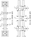
- the apparatus consists of one common exciting coil and two magnetic conductor plates with a plurality of through holes for the corresponding particle beam passing, which was proposed in US 3,715,580 and was illustrated in Fig. 1 A .
- a sub-lens such as 10 is formed between a pair of holes in the upper magnetic conductor plate 40 and the corresponding hole in the lower magnetic conductor plate 41 such as hole 4 and hole 5, a sub-lens such as 10 is formed.
- the two magnetic conductor plates 40 and 41 are the pole pieces of these sub-lenses.
- the magnetic field of the sub-lens is fundamentally different from each other in magnetic field distribution and magnetic field strength ( Fig. 1 B) .
- the field distribution of the sub-lens degenerates from axial symmetry to rotation symmetry and/or n-fold symmetry ( Fig. 1 B , Fig. 1 C) .
- the non-axisymmetric transverse field components called as high order harmonics such as dipole field (11, 12, 31, 32 in Fig. 1 B) and quadrupole field 42 ( Fig. 1 C) appear.
- the dipole field deflects the particle beams, makes the beam land on the imaging plane with an additional transverse shift, an additional tilt angle and additional aberrations.
- the quadrupole field adds astigmatism to the beam.
- the appearance of the harmonics requires the optics includes at least one additional element generating the same type field to compensate its influence.
- the magnetic flux passing through the center sub-lens 20 and peripheral sub-lens 10, 30 are not same because they are located in the area of the two magnetic conductor plates 40 and 41 with different magnetic flux. This difference makes the axisymmetric field called as round lens field of the center sub-lens 20 a little different from that of the peripheral sub-lens 10, 30. As a result, the center beam 2 passing through the center sub-lens 20 and the peripheral beams 1 and 3 passing through the peripheral sub-lenses 10 and 30 respectively are not focused at the same imaging plane ( Figure 1A ).
- US 6703624 of Haraguchi et al. nulls the round lens field difference among all the sub-lenses by changing the pole piece diameter or the pole piece gap size of the sub-lens to control the magnetic flux leakage in the individual sub-lens.
- the present invention will provide a better solution that eliminates high order harmonics along the charged particle beam path. Thereafter it provides a high throughput inspection tool for semiconductor yield enhancement.
- the present invention relates to a multi-axis magnetic lens for a charged particle beam system.
- the apparatus eliminates the undesired non-axisymmetric transverse magnetic field components called as high order harmonics from the magnetic field generated by a common excitation coil and leaves the desired axisymmetric field called as round lens field for focusing each particle beam employed within the system.
- the invention has a much broader range of applicability.
- the present invention provides several embodiments that eliminates the high order harmonics of the magnetic field on charged particle beam path.
- the high order harmonics of the magnetic field are generated by geometric symmetry variation when lens structure is altered from single axis to multi-axis.
- the first embodiment utilizes a higher permeability magnetic insert ring in each hole of each sub-lens to create permeability discontinuity.
- the magnetic insert rings inserted in the upper and lower magnetic conductor plates function as a pair of pole pieces of the sub-lens. This design weakens the non-axisymmetric distribution of magnetic scalar potential inside each magnetic ring and as a result reduces the high order harmonics of the magnetic fields.
- the second embodiment further separates the magnetic insert ring in the first embodiment from the inner sidewall of the hole by a non-magnetic material gap to form magnetic permeability discontinuity.
- the magnetic insert ring is aligned with the hole.
- the magnetic insert rings inserted in the upper and lower magnetic conductor plates function as a pair of pole pieces of the sub-lens. This design makes an efficient shield of the high order harmonics of the magnetic field within the sub-lens.
- a multilayer gap including alternately placed non-magnetic material gap and magnetic material gap makes the shielding more efficient.
- the third embodiment introduces magnetic shielding tubes that sit on/under a vacuum gap or a non-magnetic material lining outside above the upper magnetic conductor and below the lower magnetic conductor plate.
- Each magnetic shielding tube is aligned with each hole in each sub-lens to surround each charged particle beam path. This design makes an efficient shielding along the beam path of each beam from the charged particle source through the sub-lens to the imaging plane.
- a multilayer shielding can further improve the shielding effect.
- the forth embodiment of the present invention extends the magnetic insert ring on the upper magnetic conductor plate upward to the upper magnetic shielding tube and the magnetic insert ring on the lower magnetic conductor plate downward to the lower magnetic shielding tube to cover the distance between the magnetic insert ring and the magnetic shielding tube.
- the fifth embodiment of the present invention extends the magnetic insert ring on the upper magnetic conductor plate into the magnetic insert ring on the lower magnetic conductor plate as a pair of lens pole pieces. This design is for eliminating the small residual high order harmonics of the magnetic field between the upper and lower magnetic conductor plates.
- the sixth embodiment introduces two magnetic shielding houses to cap the path of all the charged particle beams respectively above the upper magnetic conductor plate and below the lower magnetic conductor plate, instead of magnetically shielding each individual charged particle beam.
- the magnetic shielding house has a top lid and a bottom plate with polarity holes that match with the corresponding incident beams and is separated by a vacuum gap or a non-magnetic material lining from the magnetic conductor plate. This design shields out most of the undesired magnetic fields inside the house, however, there still is some magnetic field leak near the opening position close to the magnetic conductor plate.
- the seventh embodiment replaces the magnetic shielding tubes or the magnetic shielding house that locates below the lower magnetic conductor plate to a magnetic shielding plate to gain a small working distance between the apparatus and the specimen.
- the eighth embodiment utilizes the thickness of the non-magnetic material gap or the multilayer gap to adjust the magnetic flux leakage in each sub-lenses, and finally makes all the sub-lenses have same round lens field.
- the present invention provides a nearly high order harmonics free environment for each charged particle beam in a multi-column charged particle beam system.
- the system could be used as condenser lens or objective lens in a multi-column apparatus.
- a charged particle optics system which comprises a pair of parallel magnetic conductor plates, a common excitation coil, a plurality of magnetic insert rings, and a plurality of gaps.
- the pair of parallel magnetic conductor plates includes a plurality of charged particle beam passing through holes, wherein each hole in the upper plate of the pair of parallel magnetic conductor plates is aligned with the corresponding hole in a lower plate of the pair of parallel magnetic conductor plates.
- Each of the plurality of magnetic insert rings is inserted in and aligned with each hole in each magnetic conductor plate.
- Each gap is inserted between the outer sidewall of each magnetic insert ring and the inner sidewall of each hole in each magnetic conductor plate.
- each sub-lens module consists of a pair of holes, the corresponding pair of magnetic insert rings functioned as a pair of pole pieces and the corresponding pair of gaps in the upper and lower magnetic conductor plates.
- the common excitation coil provides magnetic flux to the plurality of sub-lens modules, wherein each sub-lens module focuses a charged particle beam.
- Each gap has at least one vacuum layer or is filled with one non-magnetic material layer, and all the gaps may have the same or different thicknesses.
- Each gap may include a multilayer, wherein the multilayer comprises at least one magnetic layer sandwiched between two non-magnetic layers.
- the charged particle optics system can further comprise a plurality of magnetic shielding tubes, wherein each shielding tube matches each hole in each sub-lens module from outside and is separated from each magnetic conductor plate by a vacuum gap or a non-magnetic lining.
- Each magnetic insert ring in the upper plate is extended upward to cover the distance between it and the corresponding magnetic shielding tube above the upper magnetic conductor; and each magnetic insert ring in the lower plate is extended downward to cover the distance between it and the corresponding magnetic shielding tube below the lower magnetic conductor. All of the magnetic shielding tubes on the sample side of the pair of the magnetic conductor plates may be replaced by a magnetic shielding plate or a magnetic shielding house.
- the upper magnetic insert ring in the upper magnetic conductor plate is extended downward into the lower magnetic insert ring in the lower magnetic conductor plate.
- the present invention relates to a multi-axis magnetic lens for a charged particle beam system.
- the apparatus eliminates the undesired non-axisymmetric transverse magnetic field components from the magnetic field generated by a common excitation coil and leaves the desired axisymmetric field for focusing each particle beam employed within the system.
- the conventional multi electron beam lens structure or called as multi-axis lens that designed by Maekawa is illustrated in Figure 2A . It is also a basic structure, Model 1, of the present invention.
- the structure has a common excitation coil 220 covered by a coil york 230 and two magnetic conductor plates 40 and 41, wherein the magnetic conductor plate 40 is an upper plate and the magnetic conductor plate 41 is a lower plate.
- Three holes 4, 6, 8 in the upper magnetic conductor plate 40 and the corresponding holes 5, 7, 9 in the lower magnetic conductor plate 41 form three sub-lenses or sub-lens modules 10, 20 and 30, wherein each sub-lens module focuses a charged particle beam.
- the common excitation coil 220 provides magnetic flux to the sub-lens modules 10, 20 and 30.
- the coil york 230 is made of a material that has a lower permeability for example 1000.
- the magnetic conductor plates 40 and 41 are made of a material with a higher permeability for example 5000 or higher.
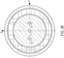
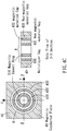
- the top view of A-A section of this system is illustrated in Figure 2B .
- the round shape structure is chosen as an example, however, the shape of the charged particle optics apparatus for a multi-column charged particle beam system in the present invention can be in any shape.
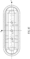
- a rectangular shaped apparatus is illustrated in Figure 2C .
- the peripheral sub-lenses 10 and 30 have a dipole field and a quadrupole field.
- Figure 2D and Figure 2E show the dipole field and quadrupole field distribution of sub-lens 30 along its optical axis 35, wherein permeability of plates 40, 41 is 5000 and coil york 230 is 1000.
- the sub-lens 20 has no dipole field because of its 2-fold symmetry.
- the present invention chooses the peripheral sub-lens 30 as an example to discuss the variation of the high order harmonics of the magnetic field in each embodiment. In this embodiment, although a dipole field and a quadrupole field in sub-lens 30 are solved, other peripheral sub-lens, such as 10 can also be applied.
- the dipole field makes the beam land on the imaging plane with an additional transverse shift, an additional tilt angle and the additional aberrations; the quadrupole field adds astigmatism to the beam; and the round lens field difference makes the center beam 2 and the peripheral beams 1 and 3 not focus at the same imaging plane.
- the first embodiment of the present invention inserts a much higher permeability magnetic insert ring into each hole of each sub-lenses to weaken the non-axisymmetric distribution of magnetic scalar potential in the sub-lens, and as a result reduces high order harmonics of the transverse magnetic field.
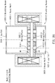
- the structure of this embodiment is illustrated in Figure 3A and called as Model 2.
- a magnetic conductor ring 310 is inserted in hole 8, in the upper plate 40 and its permeability is much higher than that of the magnetic conductor plates 40.
- the permeability of the magnetic insert ring is 100,000 versus the permeability of the magnetic conductor plate of 5,000.
- the magnetic insert rings 310 inserted in the upper and lower magnetic conductor plates function as a pair of pole pieces of the sub-lens.
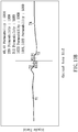
- FIG. 3B A simulation result of the dipole field distribution on the optical axis 35 of the sub-lens 30 is illustrated in Figure 3B , wherein permeability of plates 40, 41 is 5000, coil york 230 is 1000, and magnetic insert ring 310 is 100000. Inserting a magnetic conductor ring with a much higher permeability lowers the peak height of the dipole field distribution between R1 and R4.
- the magnetic insert ring can be made of Permalloy or Supermalloy.
- Permalloy is the term for a nickel iron magnetic alloy. Permalloy has a high magnetic permeability, low coercivity, near zero magnetostriction, and significant anisotropic magnetoresistance. Supermalloy is also a nickel iron based alloy with even higher magnetic permeability.
- the second embodiment of the present invention inserts a much higher permeability magnetic insert ring and a non-magnetic material gap into each hole of each sub-lens.
- the magnetic insert ring is aligned with the hole.
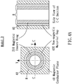
- the structure of this embodiment is illustrated in Figure 4A and called as Model 3.
- a non-magnetic material gap 420 is introduced between the inner sidewall of hole 8 and the outer sidewall of the magnetic insert ring 310.
- the non-magnetic gap 420 is a gap of vacuum, or filled with a ring of non-magnetic material such as aluminum, copper, and ceramics.
- FIG. 4B A simulation result of the dipole field distribution on the optical axis 35 of the sub-lens 30 is illustrated in Figure 4B , wherein permeability of plates 40, 41 is 5000, coil york 230 is 1000, and magnetic insert ring 310 is lowered to 5000.
- Introducing a non-magnetic material gap 420 effectively reduces the dipole field between R1 and R4.
- the permeability of the magnetic insert ring 310 needs not be very high, for example 5000 instead of 100000.
- the non-magnetic material gap 420 can efficiently help to weaken the non-axisymmetric distribution of magnetic scalar potential in the sub-lens and as a result reduce high order harmonics of the transverse magnetic field.
- Thickness of each gaps 420 in the holes 10, 20, and 30 can be the same or different.
- the magnetic insert rings 310 inserted in the upper and lower magnetic conductor plates function as a pair of pole pieces of the sub-lens.
- the thickness of the non-magnetic material gap 420 is adjusted to keep sufficiently magnetical coupling between the magnetic insert ring and the respective magnetic conductor plate 40 or 41 and at the same time provide more azimuthally isotropic distribution of magnetic scalar potential on the inner sidewall of the magnetic insert ring.
- non-magnetic material gap in the second embodiment is replaced by a multilayer gap which includes alternately placed non-magnetic material gap and magnetic material gap, the non-axisymmetric distribution of magnetic scalar potential in the sub-lens is weakened much more.
- An example of a multilayer gap model is illustrated in Figure 4C .
- two non-magnetic gaps 421, 422 and a magnetic layer 315 are interleaved between the magnetic insert ring 310 and the plates 40 or 41.
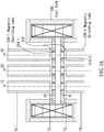
- FIG. 5A The third embodiment of the present invention is illustrated in Figure 5A .
- Two stack magnetic shielding tubes 530 respectively called as 530-1 and 530-2, are introduced to the system. This design is for removing the magnetic field in the area above the upper magnetic conductor plate 40 and below the lower magnetic conductor plate 41.
- Each magnetic shielding tube 530 with an inner diameter equal or larger than the non-magnetic material gap 420 is separated from the magnetic conductor plate 40, 41 by a non-magnetic lining 520 and aligned with the corresponding magnetic insert ring 310.
- T1 and T2 respectively correspond to the position inside and at the bottom end of the magnetic shielding tube 530-1 located above the upper magnetic conductor plates 40.
- T3 and T4 respectively correspond to the positions at the top end of and inside the magnetic shielding tube 530-2 located below the lower magnetic conductor plate 41.
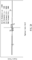
- a simulation result of the dipole field distribution on the optical axis 35 of the sub-lens 30 is illustrated in Figure 5B , wherein permeability of plates 40, 41 is 5000, coil york 230 is 1000, magnetic insert ring 310 is 5000, and magnetic shielding tubes 530 is 1000.
- the magnetic shielding tube 530 with the non-magnetic lining 520 together effectively eliminates the dipole field within the magnetic shielding tube 530 along the charged particle beam path.
- the non-magnetic lining 520 is a gap of vacuum, or made of non-magnetic material such as aluminum, copper, and ceramics.
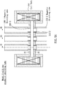
- the forth embodiment of the present invention is illustrated in Figure 6A .
- the magnetic insert ring 310-1 on the upper magnetic conductor plate 40 is extended upward to the magnetic shielding tube 530-1 and the magnetic insert ring 310-2 on the lower magnetic conductor plate 41 is extended downward to the lower magnetic shielding tube 530-2 to cover the gap created by the non-magnetic lining 520.
- the extended magnetic insert ring 310-1 and 310-2 can cover the gap either from inside or outside the magnetic shielding tube 530-1 or 530-2.
- FIG. 6B A simulation result of the dipole field distribution on the optical axis 35 of the sub-lens 30 is illustrated in Figure 6B , wherein permeability of plates 40, 41 is 5000, coil york 230 is 1000, magnetic insert ring 310 is 5000, and magnetic shielding tubes 530 is 1000.
- Figure 7 illustrates the dipole field comparison between the original structure Model 1 in Figure 2A and the present embodiment in Figure 6A . The dipole field along the beam path is effectively reduced except the bump between the two magnetic conductor plates 40 and 41.
- the fifth embodiment of the present invention is illustrated in Figure 8A .
- This design is for eliminating the small residual high order harmonics of the transverse magnetic field between the magnetic conductor plates 40 and 41.
- the magnetic insert ring 310-1 inside the upper magnetic conductor plate 40 is extended into the magnetic insert ring 310-2 inside the lower magnetic conductor plate 41.
- the magnetic insert rings inserted in the upper and lower magnetic conductor plates are functioned as a pair of pole pieces of the sub-lens.
- FIG. 8B A simulation result of the dipole field distribution on the optical axis 35 of the sub-lens 30 is illustrated in Figure 8B , wherein permeability of plates 40, 41 is 5000, coil york 230 is 1000, magnetic insert ring 310 is 5000, and magnetic shielding tubes 530 is 1000. The small residual dipole field between the magnetic conductor plates 40 and 41 is effectively removed.
- Figure 9 compares the dipole field distribution of the original structure Model 1 in Figure 2A and the current structure Model 4 in Figure 8A .
- FIG. 10A The sixth embodiment of the present invention is illustrated in Figure 10A .
- Two magnetic shielding houses 1020-1 and 1020-2 are built to cap all the sub-lenses respectively on the area above the upper magnetic conductor plate 40 and the area below the lower magnetic conductor plate 41.
- the idea is to build a common magnetic shielding for all the beams instead of building a magnetic shield tube for each individual beam.
- the simulation result of the dipole field distribution on the optical axis 35 of the sub-lens 30 is illustrated in Figure 10B , wherein permeability of plates 40, 41 is 5000, coil york 230 is 1000, magnetic insert ring 310 is 5000, house wall 1023 is 1000, and top lid1021 as well as bottom plate1022 is 5000.
- the seventh embodiment of the present invention is illustrated in Figure 11 .
- the multi-column charged particle beam optical apparatus of the present invention can be used in any charged particle system as condenser lens or objective lens.
- the excitation coil 220 and coil york 230 of the apparatus can be formed in any shape.
- the magnetic shielding tube 530-2 or the magnetic shielding house 1020-2 under the lower magnetic conductor plate 41 can be replaced by a magnetic shielding plate 1130 with plurality of holes. Each hole on the magnetic shielding plate 1130 is aligned with the corresponding hole in the lower magnetic conductor plate 41 and let the charged particle beam pass. The purpose of this replacement is to gain a small working distance between the apparatus and the specimen.
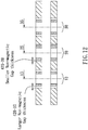
- the last embodiment of the present invention is illustrated in Figure 12 .
- the magnetic flux passing through the center sub-lens 20 is different from that of the peripheral sub-lens 30 and 10.
- This difference makes the axisymmetric field or called as round lens field of center sub-lens 20 is different from that of the peripheral sub-lens 30 and 10.
- the present invention adjusts the non-magnetic material gap 420 thickness or the multilayer gap thickness in each hole to eliminate this round lens field difference among all the sub-lenses.
- the peripheral sub-lens has a thicker non-magnetic material gap thickness in the case the peripheral sub-lens is stronger than the center sub-lens when they have the same non-magnetic material gap.
- the magnetic conductor plates and the magnetic insert rings can be made with conventional, low-cost magnetic material with moderate high permeability.
- Structural enhancements and design tunings with the non-magnetic material gap, magnetic shielding tube, house, or plate, structure relationship between the non-magnetic material gap and other magnetic shielding structures, and multilayer structure for the non-magnetic material gap can further enhance removal of dipole field and even quadrupole field.
Landscapes
- Physics & Mathematics (AREA)
- Electromagnetism (AREA)
- Chemical & Material Sciences (AREA)
- Analytical Chemistry (AREA)
- Spectroscopy & Molecular Physics (AREA)
- Engineering & Computer Science (AREA)
- General Engineering & Computer Science (AREA)
- High Energy & Nuclear Physics (AREA)
- Electron Beam Exposure (AREA)
- Testing Or Measuring Of Semiconductors Or The Like (AREA)
Applications Claiming Priority (3)
| Application Number | Priority Date | Filing Date | Title |
|---|---|---|---|
| US12/636,007 US8003953B2 (en) | 2009-12-11 | 2009-12-11 | Multi-axis magnetic lens |
| PCT/US2010/021722 WO2011071549A1 (en) | 2009-12-11 | 2010-01-22 | A multi-axis magnetic lens |
| EP10744493.7A EP2510523B1 (de) | 2009-12-11 | 2010-01-22 | Mehrachsige magnetische linse |
Related Parent Applications (1)
| Application Number | Title | Priority Date | Filing Date |
|---|---|---|---|
| EP10744493.7A Division EP2510523B1 (de) | 2009-12-11 | 2010-01-22 | Mehrachsige magnetische linse |
Publications (3)
| Publication Number | Publication Date |
|---|---|
| EP3244419A2 true EP3244419A2 (de) | 2017-11-15 |
| EP3244419A3 EP3244419A3 (de) | 2018-01-17 |
| EP3244419B1 EP3244419B1 (de) | 2023-05-31 |
Family
ID=44141870
Family Applications (2)
| Application Number | Title | Priority Date | Filing Date |
|---|---|---|---|
| EP17168514.2A Active EP3244419B1 (de) | 2009-12-11 | 2010-01-22 | Mehrachsige magnetische linse |
| EP10744493.7A Active EP2510523B1 (de) | 2009-12-11 | 2010-01-22 | Mehrachsige magnetische linse |
Family Applications After (1)
| Application Number | Title | Priority Date | Filing Date |
|---|---|---|---|
| EP10744493.7A Active EP2510523B1 (de) | 2009-12-11 | 2010-01-22 | Mehrachsige magnetische linse |
Country Status (7)
| Country | Link |
|---|---|
| US (1) | US8003953B2 (de) |
| EP (2) | EP3244419B1 (de) |
| JP (1) | JP5226132B2 (de) |
| KR (1) | KR101220837B1 (de) |
| IL (1) | IL211542A (de) |
| TW (1) | TWI389160B (de) |
| WO (1) | WO2011071549A1 (de) |
Families Citing this family (12)
| Publication number | Priority date | Publication date | Assignee | Title |
|---|---|---|---|---|
| US20100302520A1 (en) * | 2007-10-26 | 2010-12-02 | Hermes-Microvision, Inc. | Cluster e-beam lithography system |
| WO2011055520A1 (ja) * | 2009-11-06 | 2011-05-12 | 株式会社日立ハイテクノロジーズ | 電子顕微鏡 |
| US8294095B2 (en) | 2010-12-14 | 2012-10-23 | Hermes Microvision, Inc. | Apparatus of plural charged particle beams with multi-axis magnetic lens |
| US8445862B2 (en) * | 2010-12-14 | 2013-05-21 | Hermes Microvision, Inc. | Apparatus of plural charged particle beams with multi-axis magnetic lens |
| US9000394B2 (en) * | 2011-12-20 | 2015-04-07 | Hermes Microvision, Inc. | Multi-axis magnetic lens for focusing a plurality of charged particle beams |
| US8835867B2 (en) * | 2012-01-17 | 2014-09-16 | Hermes-Microvision, Inc. | Multi-axis magnetic lens for focusing a plurality of charged particle beams |
| JP6002428B2 (ja) * | 2012-04-24 | 2016-10-05 | 株式会社日立ハイテクノロジーズ | 荷電粒子線装置 |
| US9105440B2 (en) | 2013-08-30 | 2015-08-11 | Hermes Microvision, Inc. | Apparatus of plural charged particle beams with multi-axis magnetic lens |
| US9202658B2 (en) * | 2013-12-20 | 2015-12-01 | Hermes Microvision, Inc. | Multi-axis magnetic lens for focusing a plurality of charged particle beams |
| US9431209B2 (en) | 2014-08-26 | 2016-08-30 | Hermes-Microvision, Inc. | Apparatus of plural charged particle beams with multi-axis magnetic lenses |
| US10347460B2 (en) | 2017-03-01 | 2019-07-09 | Dongfang Jingyuan Electron Limited | Patterned substrate imaging using multiple electron beams |
| TWI886395B (zh) * | 2021-06-14 | 2025-06-11 | 日商紐富來科技股份有限公司 | 多帶電粒子束描繪裝置 |
Citations (5)
| Publication number | Priority date | Publication date | Assignee | Title |
|---|---|---|---|---|
| US3715580A (en) | 1970-03-04 | 1973-02-06 | Hitachi Ltd | Multi electron beam apparatus |
| US6703624B2 (en) | 2000-04-04 | 2004-03-09 | Advantest Corporation | Multi-beam exposure apparatus using a multi-axis electron lens, electron lens convergencing a plurality of electron beam and fabrication method of a semiconductor device |
| US6750455B2 (en) | 2001-07-02 | 2004-06-15 | Applied Materials, Inc. | Method and apparatus for multiple charged particle beams |
| US6777694B2 (en) | 2000-12-06 | 2004-08-17 | Advantest Corporation | Electron beam exposure system and electron lens |
| US7253417B2 (en) | 2002-12-17 | 2007-08-07 | Ict Integrated Circuit Testing Gesellschaft | Multi-axis compound lens, beam system making use of the compound lens, and method using the compound lens |
Family Cites Families (11)
| Publication number | Priority date | Publication date | Assignee | Title |
|---|---|---|---|---|
| US4209698A (en) * | 1971-12-28 | 1980-06-24 | Max-Planck-Gesellschaft Zur Forderung Der Wissenschaften E.V. | Transmission-type charged particle beam apparatus |
| DE3010814A1 (de) * | 1980-03-20 | 1981-09-24 | Siemens AG, 1000 Berlin und 8000 München | Vielstrahllinse zur erzeugung mehrerer korpuskularstrahlsonden |
| JPS61263034A (ja) * | 1985-05-16 | 1986-11-21 | Toshiba Corp | 電子顕微鏡 |
| US6787780B2 (en) * | 2000-04-04 | 2004-09-07 | Advantest Corporation | Multi-beam exposure apparatus using a multi-axis electron lens, fabrication method of a semiconductor device |
| JP2001319811A (ja) * | 2000-05-02 | 2001-11-16 | Nikon Corp | フェライトスタック用リングコア、フェライトスタック、荷電粒子線露光装置及び半導体デバイスの製造方法 |
| JP4535602B2 (ja) * | 2000-11-13 | 2010-09-01 | 株式会社アドバンテスト | 電子ビーム露光装置及び電子レンズ |
| JP2002175971A (ja) * | 2000-12-08 | 2002-06-21 | Nikon Corp | 磁気レンズ、磁気シールド体の製造方法、荷電粒子線露光装置及び半導体デバイスの製造方法 |
| JP2003077796A (ja) * | 2001-08-31 | 2003-03-14 | Nikon Corp | 荷電粒子線露光装置及び露光方法 |
| DE60235636D1 (de) * | 2002-12-17 | 2010-04-22 | Integrated Circuit Testing | it dieser Linse, und Herstellungsverfahren für diese Linse |
| JP2006079911A (ja) * | 2004-09-09 | 2006-03-23 | Hitachi High-Technologies Corp | 電子ビーム電流計測方法、電子ビーム描画装置および電子ビーム検出器 |
| US7705298B2 (en) * | 2007-10-26 | 2010-04-27 | Hermes Microvision, Inc. (Taiwan) | System and method to determine focus parameters during an electron beam inspection |
-
2009
- 2009-12-11 US US12/636,007 patent/US8003953B2/en active Active - Reinstated
- 2009-12-30 TW TW098145747A patent/TWI389160B/zh active
-
2010
- 2010-01-22 EP EP17168514.2A patent/EP3244419B1/de active Active
- 2010-01-22 KR KR1020117014889A patent/KR101220837B1/ko active Active
- 2010-01-22 WO PCT/US2010/021722 patent/WO2011071549A1/en not_active Ceased
- 2010-01-22 JP JP2011545551A patent/JP5226132B2/ja active Active
- 2010-01-22 EP EP10744493.7A patent/EP2510523B1/de active Active
-
2011
- 2011-03-03 IL IL211542A patent/IL211542A/en active IP Right Grant
Patent Citations (5)
| Publication number | Priority date | Publication date | Assignee | Title |
|---|---|---|---|---|
| US3715580A (en) | 1970-03-04 | 1973-02-06 | Hitachi Ltd | Multi electron beam apparatus |
| US6703624B2 (en) | 2000-04-04 | 2004-03-09 | Advantest Corporation | Multi-beam exposure apparatus using a multi-axis electron lens, electron lens convergencing a plurality of electron beam and fabrication method of a semiconductor device |
| US6777694B2 (en) | 2000-12-06 | 2004-08-17 | Advantest Corporation | Electron beam exposure system and electron lens |
| US6750455B2 (en) | 2001-07-02 | 2004-06-15 | Applied Materials, Inc. | Method and apparatus for multiple charged particle beams |
| US7253417B2 (en) | 2002-12-17 | 2007-08-07 | Ict Integrated Circuit Testing Gesellschaft | Multi-axis compound lens, beam system making use of the compound lens, and method using the compound lens |
Also Published As
| Publication number | Publication date |
|---|---|
| TWI389160B (zh) | 2013-03-11 |
| EP2510523A4 (de) | 2014-10-01 |
| WO2011071549A1 (en) | 2011-06-16 |
| JP5226132B2 (ja) | 2013-07-03 |
| IL211542A0 (en) | 2011-07-31 |
| JP2012507839A (ja) | 2012-03-29 |
| EP2510523B1 (de) | 2017-05-17 |
| EP3244419A3 (de) | 2018-01-17 |
| TW201120936A (en) | 2011-06-16 |
| KR101220837B1 (ko) | 2013-01-10 |
| IL211542A (en) | 2014-01-30 |
| EP2510523A1 (de) | 2012-10-17 |
| KR20110094096A (ko) | 2011-08-19 |
| US20110139996A1 (en) | 2011-06-16 |
| EP3244419B1 (de) | 2023-05-31 |
| US8003953B2 (en) | 2011-08-23 |
Similar Documents
| Publication | Publication Date | Title |
|---|---|---|
| US8003953B2 (en) | Multi-axis magnetic lens | |
| US8294095B2 (en) | Apparatus of plural charged particle beams with multi-axis magnetic lens | |
| EP3232444B1 (de) | Mehrachsige magnetische immersionsobjektivlinse | |
| US8791425B2 (en) | Multi-axis magnetic lens for focusing a plurality of charged particle beams | |
| TWI469177B (zh) | 用於帶電粒子束的鏡片系統、裝置及方法 | |
| US8158954B2 (en) | Multi-axis lens, beam system making use of the compound lens, and method of manufacturing the compound lens | |
| US9431209B2 (en) | Apparatus of plural charged particle beams with multi-axis magnetic lenses | |
| TW201442052A (zh) | 具有低軸漏洩場的永久磁鐵基高效能多軸浸沒電子透鏡陣列 | |
| US8835867B2 (en) | Multi-axis magnetic lens for focusing a plurality of charged particle beams | |
| JP5666227B2 (ja) | 色収差補正ビーム偏向器、色収差補正ビーム分離器、荷電粒子デバイス、色収差補正ビーム偏向器を動作させる方法、及び色収差補正ビーム分離器を動作させる方法 |
Legal Events
| Date | Code | Title | Description |
|---|---|---|---|
| PUAI | Public reference made under article 153(3) epc to a published international application that has entered the european phase |
Free format text: ORIGINAL CODE: 0009012 |
|
| STAA | Information on the status of an ep patent application or granted ep patent |
Free format text: STATUS: THE APPLICATION HAS BEEN PUBLISHED |
|
| AC | Divisional application: reference to earlier application |
Ref document number: 2510523 Country of ref document: EP Kind code of ref document: P |
|
| AK | Designated contracting states |
Kind code of ref document: A2 Designated state(s): AT BE BG CH CY CZ DE DK EE ES FI FR GB GR HR HU IE IS IT LI LT LU LV MC MK MT NL NO PL PT RO SE SI SK SM TR |
|
| PUAL | Search report despatched |
Free format text: ORIGINAL CODE: 0009013 |
|
| AK | Designated contracting states |
Kind code of ref document: A3 Designated state(s): AT BE BG CH CY CZ DE DK EE ES FI FR GB GR HR HU IE IS IT LI LT LU LV MC MK MT NL NO PL PT RO SE SI SK SM TR |
|
| RIC1 | Information provided on ipc code assigned before grant |
Ipc: G21K 1/08 20060101AFI20171214BHEP Ipc: H01J 37/141 20060101ALI20171214BHEP |
|
| STAA | Information on the status of an ep patent application or granted ep patent |
Free format text: STATUS: REQUEST FOR EXAMINATION WAS MADE |
|
| 17P | Request for examination filed |
Effective date: 20180608 |
|
| RBV | Designated contracting states (corrected) |
Designated state(s): AT BE BG CH CY CZ DE DK EE ES FI FR GB GR HR HU IE IS IT LI LT LU LV MC MK MT NL NO PL PT RO SE SI SK SM TR |
|
| RAP1 | Party data changed (applicant data changed or rights of an application transferred) |
Owner name: ASML NETHERLANDS B.V. |
|
| STAA | Information on the status of an ep patent application or granted ep patent |
Free format text: STATUS: EXAMINATION IS IN PROGRESS |
|
| 17Q | First examination report despatched |
Effective date: 20210628 |
|
| GRAP | Despatch of communication of intention to grant a patent |
Free format text: ORIGINAL CODE: EPIDOSNIGR1 |
|
| STAA | Information on the status of an ep patent application or granted ep patent |
Free format text: STATUS: GRANT OF PATENT IS INTENDED |
|
| INTG | Intention to grant announced |
Effective date: 20220801 |
|
| GRAJ | Information related to disapproval of communication of intention to grant by the applicant or resumption of examination proceedings by the epo deleted |
Free format text: ORIGINAL CODE: EPIDOSDIGR1 |
|
| STAA | Information on the status of an ep patent application or granted ep patent |
Free format text: STATUS: EXAMINATION IS IN PROGRESS |
|
| GRAP | Despatch of communication of intention to grant a patent |
Free format text: ORIGINAL CODE: EPIDOSNIGR1 |
|
| STAA | Information on the status of an ep patent application or granted ep patent |
Free format text: STATUS: GRANT OF PATENT IS INTENDED |
|
| INTC | Intention to grant announced (deleted) | ||
| INTG | Intention to grant announced |
Effective date: 20221219 |
|
| GRAS | Grant fee paid |
Free format text: ORIGINAL CODE: EPIDOSNIGR3 |
|
| GRAA | (expected) grant |
Free format text: ORIGINAL CODE: 0009210 |
|
| STAA | Information on the status of an ep patent application or granted ep patent |
Free format text: STATUS: THE PATENT HAS BEEN GRANTED |
|
| AC | Divisional application: reference to earlier application |
Ref document number: 2510523 Country of ref document: EP Kind code of ref document: P |
|
| AK | Designated contracting states |
Kind code of ref document: B1 Designated state(s): AT BE BG CH CY CZ DE DK EE ES FI FR GB GR HR HU IE IS IT LI LT LU LV MC MK MT NL NO PL PT RO SE SI SK SM TR |
|
| REG | Reference to a national code |
Ref country code: GB Ref legal event code: FG4D Ref country code: CH Ref legal event code: EP |
|
| REG | Reference to a national code |
Ref country code: DE Ref legal event code: R096 Ref document number: 602010068824 Country of ref document: DE |
|
| P01 | Opt-out of the competence of the unified patent court (upc) registered |
Effective date: 20230414 |
|
| REG | Reference to a national code |
Ref country code: AT Ref legal event code: REF Ref document number: 1571446 Country of ref document: AT Kind code of ref document: T Effective date: 20230615 |
|
| REG | Reference to a national code |
Ref country code: IE Ref legal event code: FG4D |
|
| REG | Reference to a national code |
Ref country code: LT Ref legal event code: MG9D |
|
| REG | Reference to a national code |
Ref country code: NL Ref legal event code: MP Effective date: 20230531 |
|
| REG | Reference to a national code |
Ref country code: AT Ref legal event code: MK05 Ref document number: 1571446 Country of ref document: AT Kind code of ref document: T Effective date: 20230531 |
|
| PG25 | Lapsed in a contracting state [announced via postgrant information from national office to epo] |
Ref country code: SE Free format text: LAPSE BECAUSE OF FAILURE TO SUBMIT A TRANSLATION OF THE DESCRIPTION OR TO PAY THE FEE WITHIN THE PRESCRIBED TIME-LIMIT Effective date: 20230531 Ref country code: NO Free format text: LAPSE BECAUSE OF FAILURE TO SUBMIT A TRANSLATION OF THE DESCRIPTION OR TO PAY THE FEE WITHIN THE PRESCRIBED TIME-LIMIT Effective date: 20230831 Ref country code: ES Free format text: LAPSE BECAUSE OF FAILURE TO SUBMIT A TRANSLATION OF THE DESCRIPTION OR TO PAY THE FEE WITHIN THE PRESCRIBED TIME-LIMIT Effective date: 20230531 Ref country code: AT Free format text: LAPSE BECAUSE OF FAILURE TO SUBMIT A TRANSLATION OF THE DESCRIPTION OR TO PAY THE FEE WITHIN THE PRESCRIBED TIME-LIMIT Effective date: 20230531 |
|
| PG25 | Lapsed in a contracting state [announced via postgrant information from national office to epo] |
Ref country code: PL Free format text: LAPSE BECAUSE OF FAILURE TO SUBMIT A TRANSLATION OF THE DESCRIPTION OR TO PAY THE FEE WITHIN THE PRESCRIBED TIME-LIMIT Effective date: 20230531 Ref country code: NL Free format text: LAPSE BECAUSE OF FAILURE TO SUBMIT A TRANSLATION OF THE DESCRIPTION OR TO PAY THE FEE WITHIN THE PRESCRIBED TIME-LIMIT Effective date: 20230531 Ref country code: LV Free format text: LAPSE BECAUSE OF FAILURE TO SUBMIT A TRANSLATION OF THE DESCRIPTION OR TO PAY THE FEE WITHIN THE PRESCRIBED TIME-LIMIT Effective date: 20230531 Ref country code: LT Free format text: LAPSE BECAUSE OF FAILURE TO SUBMIT A TRANSLATION OF THE DESCRIPTION OR TO PAY THE FEE WITHIN THE PRESCRIBED TIME-LIMIT Effective date: 20230531 Ref country code: IS Free format text: LAPSE BECAUSE OF FAILURE TO SUBMIT A TRANSLATION OF THE DESCRIPTION OR TO PAY THE FEE WITHIN THE PRESCRIBED TIME-LIMIT Effective date: 20230930 Ref country code: HR Free format text: LAPSE BECAUSE OF FAILURE TO SUBMIT A TRANSLATION OF THE DESCRIPTION OR TO PAY THE FEE WITHIN THE PRESCRIBED TIME-LIMIT Effective date: 20230531 Ref country code: GR Free format text: LAPSE BECAUSE OF FAILURE TO SUBMIT A TRANSLATION OF THE DESCRIPTION OR TO PAY THE FEE WITHIN THE PRESCRIBED TIME-LIMIT Effective date: 20230901 |
|
| PG25 | Lapsed in a contracting state [announced via postgrant information from national office to epo] |
Ref country code: FI Free format text: LAPSE BECAUSE OF FAILURE TO SUBMIT A TRANSLATION OF THE DESCRIPTION OR TO PAY THE FEE WITHIN THE PRESCRIBED TIME-LIMIT Effective date: 20230531 |
|
| PG25 | Lapsed in a contracting state [announced via postgrant information from national office to epo] |
Ref country code: SK Free format text: LAPSE BECAUSE OF FAILURE TO SUBMIT A TRANSLATION OF THE DESCRIPTION OR TO PAY THE FEE WITHIN THE PRESCRIBED TIME-LIMIT Effective date: 20230531 |
|
| PG25 | Lapsed in a contracting state [announced via postgrant information from national office to epo] |
Ref country code: SM Free format text: LAPSE BECAUSE OF FAILURE TO SUBMIT A TRANSLATION OF THE DESCRIPTION OR TO PAY THE FEE WITHIN THE PRESCRIBED TIME-LIMIT Effective date: 20230531 Ref country code: SK Free format text: LAPSE BECAUSE OF FAILURE TO SUBMIT A TRANSLATION OF THE DESCRIPTION OR TO PAY THE FEE WITHIN THE PRESCRIBED TIME-LIMIT Effective date: 20230531 Ref country code: RO Free format text: LAPSE BECAUSE OF FAILURE TO SUBMIT A TRANSLATION OF THE DESCRIPTION OR TO PAY THE FEE WITHIN THE PRESCRIBED TIME-LIMIT Effective date: 20230531 Ref country code: PT Free format text: LAPSE BECAUSE OF FAILURE TO SUBMIT A TRANSLATION OF THE DESCRIPTION OR TO PAY THE FEE WITHIN THE PRESCRIBED TIME-LIMIT Effective date: 20231002 Ref country code: EE Free format text: LAPSE BECAUSE OF FAILURE TO SUBMIT A TRANSLATION OF THE DESCRIPTION OR TO PAY THE FEE WITHIN THE PRESCRIBED TIME-LIMIT Effective date: 20230531 Ref country code: DK Free format text: LAPSE BECAUSE OF FAILURE TO SUBMIT A TRANSLATION OF THE DESCRIPTION OR TO PAY THE FEE WITHIN THE PRESCRIBED TIME-LIMIT Effective date: 20230531 Ref country code: CZ Free format text: LAPSE BECAUSE OF FAILURE TO SUBMIT A TRANSLATION OF THE DESCRIPTION OR TO PAY THE FEE WITHIN THE PRESCRIBED TIME-LIMIT Effective date: 20230531 |
|
| REG | Reference to a national code |
Ref country code: DE Ref legal event code: R097 Ref document number: 602010068824 Country of ref document: DE |
|
| PLBE | No opposition filed within time limit |
Free format text: ORIGINAL CODE: 0009261 |
|
| STAA | Information on the status of an ep patent application or granted ep patent |
Free format text: STATUS: NO OPPOSITION FILED WITHIN TIME LIMIT |
|
| PG25 | Lapsed in a contracting state [announced via postgrant information from national office to epo] |
Ref country code: SI Free format text: LAPSE BECAUSE OF FAILURE TO SUBMIT A TRANSLATION OF THE DESCRIPTION OR TO PAY THE FEE WITHIN THE PRESCRIBED TIME-LIMIT Effective date: 20230531 |
|
| 26N | No opposition filed |
Effective date: 20240301 |
|
| PG25 | Lapsed in a contracting state [announced via postgrant information from national office to epo] |
Ref country code: SI Free format text: LAPSE BECAUSE OF FAILURE TO SUBMIT A TRANSLATION OF THE DESCRIPTION OR TO PAY THE FEE WITHIN THE PRESCRIBED TIME-LIMIT Effective date: 20230531 Ref country code: IT Free format text: LAPSE BECAUSE OF FAILURE TO SUBMIT A TRANSLATION OF THE DESCRIPTION OR TO PAY THE FEE WITHIN THE PRESCRIBED TIME-LIMIT Effective date: 20230531 |
|
| PG25 | Lapsed in a contracting state [announced via postgrant information from national office to epo] |
Ref country code: MC Free format text: LAPSE BECAUSE OF FAILURE TO SUBMIT A TRANSLATION OF THE DESCRIPTION OR TO PAY THE FEE WITHIN THE PRESCRIBED TIME-LIMIT Effective date: 20230531 |
|
| PG25 | Lapsed in a contracting state [announced via postgrant information from national office to epo] |
Ref country code: MC Free format text: LAPSE BECAUSE OF FAILURE TO SUBMIT A TRANSLATION OF THE DESCRIPTION OR TO PAY THE FEE WITHIN THE PRESCRIBED TIME-LIMIT Effective date: 20230531 |
|
| REG | Reference to a national code |
Ref country code: CH Ref legal event code: PL |
|
| PG25 | Lapsed in a contracting state [announced via postgrant information from national office to epo] |
Ref country code: LU Free format text: LAPSE BECAUSE OF NON-PAYMENT OF DUE FEES Effective date: 20240122 |
|
| GBPC | Gb: european patent ceased through non-payment of renewal fee |
Effective date: 20240122 |
|
| PG25 | Lapsed in a contracting state [announced via postgrant information from national office to epo] |
Ref country code: LU Free format text: LAPSE BECAUSE OF NON-PAYMENT OF DUE FEES Effective date: 20240122 |
|
| PG25 | Lapsed in a contracting state [announced via postgrant information from national office to epo] |
Ref country code: GB Free format text: LAPSE BECAUSE OF NON-PAYMENT OF DUE FEES Effective date: 20240122 |
|
| PG25 | Lapsed in a contracting state [announced via postgrant information from national office to epo] |
Ref country code: BE Free format text: LAPSE BECAUSE OF NON-PAYMENT OF DUE FEES Effective date: 20240131 |
|
| PG25 | Lapsed in a contracting state [announced via postgrant information from national office to epo] |
Ref country code: FR Free format text: LAPSE BECAUSE OF NON-PAYMENT OF DUE FEES Effective date: 20240131 |
|
| PG25 | Lapsed in a contracting state [announced via postgrant information from national office to epo] |
Ref country code: CH Free format text: LAPSE BECAUSE OF NON-PAYMENT OF DUE FEES Effective date: 20240131 |
|
| PG25 | Lapsed in a contracting state [announced via postgrant information from national office to epo] |
Ref country code: GB Free format text: LAPSE BECAUSE OF NON-PAYMENT OF DUE FEES Effective date: 20240122 Ref country code: FR Free format text: LAPSE BECAUSE OF NON-PAYMENT OF DUE FEES Effective date: 20240131 Ref country code: CH Free format text: LAPSE BECAUSE OF NON-PAYMENT OF DUE FEES Effective date: 20240131 Ref country code: BE Free format text: LAPSE BECAUSE OF NON-PAYMENT OF DUE FEES Effective date: 20240131 |
|
| REG | Reference to a national code |
Ref country code: BE Ref legal event code: MM Effective date: 20240131 |
|
| PG25 | Lapsed in a contracting state [announced via postgrant information from national office to epo] |
Ref country code: BG Free format text: LAPSE BECAUSE OF FAILURE TO SUBMIT A TRANSLATION OF THE DESCRIPTION OR TO PAY THE FEE WITHIN THE PRESCRIBED TIME-LIMIT Effective date: 20230531 |
|
| PG25 | Lapsed in a contracting state [announced via postgrant information from national office to epo] |
Ref country code: BG Free format text: LAPSE BECAUSE OF FAILURE TO SUBMIT A TRANSLATION OF THE DESCRIPTION OR TO PAY THE FEE WITHIN THE PRESCRIBED TIME-LIMIT Effective date: 20230531 |
|
| PG25 | Lapsed in a contracting state [announced via postgrant information from national office to epo] |
Ref country code: IE Free format text: LAPSE BECAUSE OF NON-PAYMENT OF DUE FEES Effective date: 20240122 |
|
| PG25 | Lapsed in a contracting state [announced via postgrant information from national office to epo] |
Ref country code: IE Free format text: LAPSE BECAUSE OF NON-PAYMENT OF DUE FEES Effective date: 20240122 |
|
| PG25 | Lapsed in a contracting state [announced via postgrant information from national office to epo] |
Ref country code: CY Free format text: LAPSE BECAUSE OF FAILURE TO SUBMIT A TRANSLATION OF THE DESCRIPTION OR TO PAY THE FEE WITHIN THE PRESCRIBED TIME-LIMIT; INVALID AB INITIO Effective date: 20100122 |
|
| PG25 | Lapsed in a contracting state [announced via postgrant information from national office to epo] |
Ref country code: HU Free format text: LAPSE BECAUSE OF FAILURE TO SUBMIT A TRANSLATION OF THE DESCRIPTION OR TO PAY THE FEE WITHIN THE PRESCRIBED TIME-LIMIT; INVALID AB INITIO Effective date: 20100122 |
|
| PG25 | Lapsed in a contracting state [announced via postgrant information from national office to epo] |
Ref country code: TR Free format text: LAPSE BECAUSE OF FAILURE TO SUBMIT A TRANSLATION OF THE DESCRIPTION OR TO PAY THE FEE WITHIN THE PRESCRIBED TIME-LIMIT Effective date: 20230531 |
|
| PGFP | Annual fee paid to national office [announced via postgrant information from national office to epo] |
Ref country code: DE Payment date: 20260127 Year of fee payment: 17 |