EP3244539A1 - Amplitudendetektion mit kompensation - Google Patents
Amplitudendetektion mit kompensation Download PDFInfo
- Publication number
- EP3244539A1 EP3244539A1 EP17169981.2A EP17169981A EP3244539A1 EP 3244539 A1 EP3244539 A1 EP 3244539A1 EP 17169981 A EP17169981 A EP 17169981A EP 3244539 A1 EP3244539 A1 EP 3244539A1
- Authority
- EP
- European Patent Office
- Prior art keywords
- transistors
- pair
- circuit
- voltage
- coupled
- Prior art date
- Legal status (The legal status is an assumption and is not a legal conclusion. Google has not performed a legal analysis and makes no representation as to the accuracy of the status listed.)
- Withdrawn
Links
- 238000001514 detection method Methods 0.000 title description 21
- 239000003990 capacitor Substances 0.000 description 12
- 238000010586 diagram Methods 0.000 description 8
- 238000000034 method Methods 0.000 description 4
- 230000000694 effects Effects 0.000 description 2
- 238000012986 modification Methods 0.000 description 2
- 230000004048 modification Effects 0.000 description 2
- 239000000919 ceramic Substances 0.000 description 1
- 238000006243 chemical reaction Methods 0.000 description 1
- 239000013078 crystal Substances 0.000 description 1
- 230000003247 decreasing effect Effects 0.000 description 1
- 238000001914 filtration Methods 0.000 description 1
- 239000000463 material Substances 0.000 description 1
- 230000010363 phase shift Effects 0.000 description 1
Images


Classifications
-
- H—ELECTRICITY
- H03—ELECTRONIC CIRCUITRY
- H03B—GENERATION OF OSCILLATIONS, DIRECTLY OR BY FREQUENCY-CHANGING, BY CIRCUITS EMPLOYING ACTIVE ELEMENTS WHICH OPERATE IN A NON-SWITCHING MANNER; GENERATION OF NOISE BY SUCH CIRCUITS
- H03B5/00—Generation of oscillations using amplifier with regenerative feedback from output to input
- H03B5/08—Generation of oscillations using amplifier with regenerative feedback from output to input with frequency-determining element comprising lumped inductance and capacitance
- H03B5/12—Generation of oscillations using amplifier with regenerative feedback from output to input with frequency-determining element comprising lumped inductance and capacitance active element in amplifier being semiconductor device
- H03B5/1206—Generation of oscillations using amplifier with regenerative feedback from output to input with frequency-determining element comprising lumped inductance and capacitance active element in amplifier being semiconductor device using multiple transistors for amplification
-
- H—ELECTRICITY
- H03—ELECTRONIC CIRCUITRY
- H03K—PULSE TECHNIQUE
- H03K5/00—Manipulating of pulses not covered by one of the other main groups of this subclass
- H03K5/22—Circuits having more than one input and one output for comparing pulses or pulse trains with each other according to input signal characteristics, e.g. slope, integral
-
- H—ELECTRICITY
- H03—ELECTRONIC CIRCUITRY
- H03B—GENERATION OF OSCILLATIONS, DIRECTLY OR BY FREQUENCY-CHANGING, BY CIRCUITS EMPLOYING ACTIVE ELEMENTS WHICH OPERATE IN A NON-SWITCHING MANNER; GENERATION OF NOISE BY SUCH CIRCUITS
- H03B5/00—Generation of oscillations using amplifier with regenerative feedback from output to input
- H03B5/08—Generation of oscillations using amplifier with regenerative feedback from output to input with frequency-determining element comprising lumped inductance and capacitance
- H03B5/12—Generation of oscillations using amplifier with regenerative feedback from output to input with frequency-determining element comprising lumped inductance and capacitance active element in amplifier being semiconductor device
- H03B5/1228—Generation of oscillations using amplifier with regenerative feedback from output to input with frequency-determining element comprising lumped inductance and capacitance active element in amplifier being semiconductor device the amplifier comprising one or more field effect transistors
-
- H—ELECTRICITY
- H03—ELECTRONIC CIRCUITRY
- H03K—PULSE TECHNIQUE
- H03K5/00—Manipulating of pulses not covered by one of the other main groups of this subclass
- H03K5/22—Circuits having more than one input and one output for comparing pulses or pulse trains with each other according to input signal characteristics, e.g. slope, integral
- H03K5/24—Circuits having more than one input and one output for comparing pulses or pulse trains with each other according to input signal characteristics, e.g. slope, integral the characteristic being amplitude
- H03K5/2472—Circuits having more than one input and one output for comparing pulses or pulse trains with each other according to input signal characteristics, e.g. slope, integral the characteristic being amplitude using field effect transistors
- H03K5/2481—Circuits having more than one input and one output for comparing pulses or pulse trains with each other according to input signal characteristics, e.g. slope, integral the characteristic being amplitude using field effect transistors with at least one differential stage
-
- H—ELECTRICITY
- H03—ELECTRONIC CIRCUITRY
- H03L—AUTOMATIC CONTROL, STARTING, SYNCHRONISATION OR STABILISATION OF GENERATORS OF ELECTRONIC OSCILLATIONS OR PULSES
- H03L5/00—Automatic control of voltage, current, or power
Definitions
- This invention relates to amplitude detection circuits and systems that utilize amplitude detection circuits.
- Amplitude detection circuits can be used to detect the amplitude voltage of a signal.
- an amplitude detection circuit can be used to detect the amplitude of an oscillator output signal.
- the amplitude detected by an amplitude detector can be compared with a reference value to adjust the amplitude of the oscillator circuit.
- a circuit comprising: an amplitude detector comprising: an input to receive a signal having an amplitude voltage; a first pair of transistors configured in parallel, the input is coupled to a control terminal of at least one transistor of the first pair; a first node providing a voltage indicative of the amplitude voltage, wherein the first node is in series with each of the first pair of transistors; a compensation circuit comprising: a second pair of transistors configured in parallel; a second node, the second node is coupled in series with each transistor of the second pair; an amplifier including a first amplifier input coupled to the first node and a second amplifier input coupled to the second node.
- a voltage differential across control terminals of the second pair of transistors may be proportional to the amplitude voltage of the signal.
- An output of the amplifier may be configured to adjust a voltage of the second amplifier input to match a voltage of the first amplifier input.
- An output of the amplifier may be configured to adjust a voltage of the first amplifier input to match a voltage of the second amplifier input.
- the circuit of may further comprise an amplitude setting circuit, where each control terminal of the second pair of transistors is biased at a voltage set by the amplitude setting circuit.
- the amplitude setting circuit may produce a current through a set of devices coupled in series in a current path, wherein the current is indicative of a desired amplitude voltage, wherein a control terminal of one transistor of the second pair of transistors is biased at one node of the current path and a control terminal of a second transistor of the second pair of transistors is biased at another node of the current path.
- the first pair of transistors and the second pair of transistors are characterized as MOSFETs.
- the first pair of transistors may be matched with the second pair of transistors.
- the first pair of transistors may be coupled in series with a first current path, the first node may be a node of the first current path, the first current path may include a first current source coupled in series with the first pair of transistors and the first node;
- the second pair of transistors may be coupled in series with a second current path, the second node may be a node of the second current path, the second current path may include a second current source coupled in series with the second pair of transistors and the second node.
- the first current source and the second current source may be equivalent.
- the first current path may include a first resistive element in the first current path coupled between the first pair of transistors and the first node;
- the second current path may include a second resistive element in the second current path coupled between the second pair of transistors and the second node.
- the second current source may produce X times the current as the first current source and the second resistive element may be 1/X times the resistance of the first resistive element.
- the circuit may further comprise: a filter circuit having an input coupled to the first node and an output coupled to the first amplifier input, the first node is coupled to the first amplifier input through the filter circuit, the filter circuit configured to filter out higher frequency components of the voltage indicative of the amplitude voltage.
- the signal may be a differential signal, wherein the input includes a first input terminal coupled to a control terminal of a first transistor of the first pair of transistors, the input includes a second input terminal coupled to a control terminal of a second transistor of the first pair of transistors.
- a control terminal of a first transistor of the first pair of transistors may be coupled to a bias voltage source through a first resistive element, a control terminal of a second transistor of the first pair of transistors may be coupled to the bias voltage source, a control terminal of a transistor of the second pair of transistors may be coupled to the bias voltage source, wherein a current terminal of each transistor of the first pair of transistors and the second pair of transistors is coupled to a high voltage supply terminal, wherein a supply voltage of the high voltage supply terminal is higher than a bias voltage of the bias voltage source.
- the compensation circuit may include a second amplifier having a first input coupled to the bias voltage source and an output coupled to a control terminal of a transistor of the second pair of transistors to control a conductivity of the transistor of the second pair of transistors.
- the circuit may further comprise: a transistor having a control terminal, wherein tan output of the amplifier is coupled to the control terminal to control a conductivity of the transistor, wherein the circuit includes an output providing an indication of the amplitude voltage of the signal, wherein the output is coupled to a current terminal of the transistor.
- the signal may be a single ended signal, wherein the input includes an input terminal coupled to a control input of a first transistor of the first pair of transistors, wherein a control terminal of a second transistor of the first pair of transistors is coupled to a voltage reference source, wherein a control terminal of a transistor of the second pair of transistors is coupled to the voltage reference source.
- the input of the amplitude detector may be coupled to an output of an oscillator circuit to receive an oscillator signal, wherein the signal is the oscillator signal, and an output of the amplifier controls an amplitude voltage of the oscillator signal.
- an oscillator circuit comprising: an oscillator having an output to produce an oscillator signal and a control input to control an amplitude of the oscillator signal; an amplitude detector comprising: a first current path, the first current path including a first node to provide a voltage indicative of an amplitude of the oscillator signal; a first pair of transistors, each transistor of the first pair of transistors is coupled in series with the first current path, the first pair of transistors is coupled in parallel; an input to receive the oscillator signal, the input includes a first input terminal coupled to a control terminal of a transistor of the first pair of transistors; a compensation circuit comprising: a second current path; a second pair of transistors, each transistor of the second pair of transistors is coupled in series with the second current path, the second pair of transistors is coupled in parallel, the second pair of transistors includes a first transistor having a control terminal and a second transistor having a control terminal; a circuit for setting a voltage differential between the
- an amplitude detection circuit can include a compensation circuit to compensate for inefficiencies, non ideal characteristics, temperature variation, and/or process variation of the devices of the amplitude detection circuit.
- Amplitude detectors are utilized for detecting the amplitude of a signal. They can be used in oscillator systems (e.g. clocks) to control the amplitude voltage of the oscillator signal. Based on the signal type and configuration, some amplitude detectors can detect the peak voltage of a signal (e.g. a peak detector). However, with other types of amplitude detection circuits, the actual amplitude detected by the detection circuit for some signals (e.g. a sinusoidal signal) is less than the peak voltage (e.g. the RMS voltage of the signal).
- an amplitude detector should accurately measure the amplitude voltage of a signal even at relatively low voltages or high frequencies.
- non ideal characteristics of the devices of the amplitude detector can cause the circuit to deviate from ideal performance.
- amplitude detectors that are implemented with MOSFETS can suffer from issues due to the relatively lower transconductance of a MOSFET.
- transistors coupled in parallel for receiving differential input signals may undesirably conduct simultaneously during a portion of an oscillator signal cycle.
- the effects of simultaneous transistor conduction is worse in a detector circuit implemented with MOSFETS due to their lower transconductance.
- These non-ideal characteristics of a MOSFET can affect an amplitude detector in the detection of an amplitude of a low voltage signal (e.g. 300 mV and lower).
- an amplitude detection circuit includes a compensation circuit that includes devices equivalent to devices of the amplitude detector to compensate for the non ideal characteristics of the devices.
- both the amplitude detector and the compensation circuit include transistor pairs coupled in parallel that each produce a voltage that is used to provide a signal indicative of the amplitude voltage.
- that signal is used to adjust one of the voltages of the amplitude detector or compensation circuit to equal the other voltage in order to compensate for the output of the system.
- the amplitude voltage of the oscillator is proportional to the voltage differential across the control terminals of the transistor pair of the compensation circuit during a steady state condition.
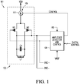
- FIG. 1 is a circuit diagram of an oscillator circuit 101 according to one embodiment of the present invention.
- Oscillator circuit 101 includes an oscillator 103 that provides at its output, a differential oscillating signal (OSC+, OSC-) at a frequency determined by the size of capacitor C1 and inductor L.
- the amplitude of the oscillator output is controlled by a control signal (CONTROL) provided to a current source 111 of oscillator circuit 103 to control the amount of current flowing to the oscillator.
- CONTROL control signal
- the oscillator signal may be used as a clocking signal by other circuitry (not shown) of a system that implements oscillator circuit 101.
- oscillator 103 provides a sinusoidal wave differential oscillator signal, but in other embodiments, may provide another type of oscillator signal such as a square wave signal. Also in other embodiments, oscillator circuit 103 may provide a single ended signal. In the embodiment shown, oscillator 103 is an LC type oscillator, but in other embodiments, may be another type of oscillator such as e.g. a crystal oscillator, a ceramic resonator oscillator, a phase-shift oscillator, or a negative resistance oscillator.
- the control signal is provided from an amplitude detector and control circuit 109.
- Circuit 109 receives the oscillator output from oscillator circuit 103, a voltage reference (VREF), a voltage reference (VB), and a digital control signal (DIGITAL CONTROL).
- VREF and VB are each provided from a voltage reference source such as a band gap circuit (not shown), but may be provided from another types of voltage reference sources (e.g. a power supply) in other embodiments.
- the tolerances for VREF are more stringent than for VB.
- the digital control signal is indicative of a desired amplitude of the oscillator signal.
- the digital control signal is provided by a microcontroller (not shown), but may be provided from other sources (e.g.
- circuit 109 does not receive a digital control signal, wherein the desired amplitude is based on Vref.
- oscillator signal has a frequency of 2GHz but may have other frequencies in other embodiments.
- Circuit 109 detects the amplitude of the oscillator signal and compares it to a compared voltage value that is based on the VREF signal and a digital control signal to produce the control signal for adjusting the amplitude of the oscillator signal to match the desired amplitude as indicated by the digital control signal.
- the compared voltage value is compensated to account for non-ideal characteristics and process variations of the devices of amplitude detection and control circuit 109.
- FIG. 2 is a circuit diagram of an amplitude detector and control circuit 109 according to one embodiment of the present invention.
- Circuit 109 includes an amplitude setting circuit 201, and an amplitude detection circuit 203, and a compensation circuit 205 that produces the control signal that is provided to oscillator 103.
- Amplitude setting circuit 201 receives the VREF voltage and the digital control signal and produces a current through resistors 245 and 247 that produces voltages (VC1 and VC2), which are indicative of a desired amplitude of the oscillator signal.
- the amplitude of the oscillator circuit is proportional to the voltage differential between VC1 and VC2 in a steady state operation of circuit 101.
- the VREF voltage is converted to a current (I REF ) by V/I converter circuit 209 which includes amplifier 204, resister 208, and NMOS transistor 206.
- Circuit 201 includes a controlled current mirror 211 that receives the digital control signal and multiples I REF by the number of enabled current paths as per the digital control value that is received by circuit 201.
- each current path of current mirror 211 includes a PMOS transistor that is controlled by a signal line of the digital control signal. The greater the number of enabled current paths, the higher the resultant multiplied current (I DC ), and the greater the desired oscillator amplitude that will be produced.
- Circuit 201 also includes a current mirror of transistors 213, 217, 219, and 221 that mirror current I DC to produce current I F .
- Transistor 219 serves as source for the current mirror and transistor 221 serves as a sink for the current mirror.
- Current IF is indicative of the desired oscillator amplitude.
- the voltage differential between VC1 and VC2 may be generated by other types of circuits including circuits utilizing differential amplifiers.
- circuit 109 includes an amplitude detector circuit 203.
- Amplitude detector circuit 203 includes capacitors 225 and 223, resistors 227 and 220, transistors 231 and 233 (which are coupled in parallel) resistor 229, current source 235, and filter 237.
- Capacitors 225 and 223 act to block DC bias signals thereby only allowing the oscillating signal to pass to transistors 231 and 233.
- transistor 231 or 233 will be made more conductive to pull the voltage at node VT high. The higher the amplitude of the oscillator signal, the more conductive transistors 231 and 233 will be to pull up the voltage of node VT.
- the gates of transistors 231 and 233 are biased at voltage VB through resistors 277 and 220, respectively.
- VB is provided from a reference voltage source (not shown).
- VB is 1.0 volts which is less than VDD (e.g. 1.2 volts).
- VB is set at a level such that MOSFET transistors 231 and 233 will operate in their saturation regions at the possible amplitude ranges of the oscillator circuit.
- VB may be set at other voltages in other embodiments.
- Node VT is located in series with resistor 229 and current source 235 to provide a VM signal whose voltage is indicative of the measured amplitude of the oscillator signal.
- the VM signal is filtered by filter 237 to remove the higher frequency components to provide for a more stable voltage signal (VMF).
- Filter 237 includes capacitor 239, resistor 241 and capacitor 243.
- filter 237 filters out all components from the VM signal above 10 MHz hertz.
- the cutoff frequency is 100 times lower than the frequency of the oscillator signal.
- Resistor 229 and filter 237 also act to reduce the effect of high frequency components of the voltage at node VT on current source 235.
- Circuit 109 includes a comparison circuit 205.
- Comparison circuit 205 includes resistors 245, 247, and 253, NMOS transistors 249 and 251, current source 259, and amplifier 257.
- comparison circuit 205 produces a voltage at node 260 from current I F that is indicative of the desired amplitude and compares it with the VMF signal produced by the amplitude detector circuit 203 (and filtered by filter 237) to adjust the control signal so that the measured amplitude of the oscillator signal (as measured by circuit 203) matches the desired amplitude (as indicated by circuit 201).
- Circuit 205 converts the current I F to a voltage at node 260 with the use of two NMOS transistors 249 and 251.
- the greater the current I F (indicating a higher desired amplitude), the higher the voltage at node V C1 .
- the higher the voltage V C1 the more conductive transistor 251 is to pull node 260 higher towards VDD.
- the lower the current I F the lower voltage V C1 is to voltage VB. Accordingly, the voltage at node 260 is decreased in that transistor 251 is not as conductive and provides a greater resistance to reduce the voltage at node 260.
- transistors 231, 233, 249 and 251 are "equivalent.” Equivalent means that the transistors are the same size or substantially the same size. Also, current sources 235 and 259 are equivalent (they are implemented with the same type of devices and produce the same current or substantially the same current). In one embodiment, current sources are designed to produce 10 uA of current. Also, resistors 253 and 229 are equivalent in that they are the same resistance or substantially the same resistance and are the same type of device (e.g. a poly resistor or a MOSFET configured as a resistor). Resistors 245 and 247 are also equivalent. Furthermore, resistor 208 is made out of the same material as resistors 245 and 247.
- transistor 231 and 233 are "matched" with transistors 249 and 251.
- Matched means that the effective size of one transistor is a multiple integer size of the other transistor.
- Two transistors that are equivalent are also considered matched.
- the matched feature can be obtained by either making the channel of the larger transistor physically wider or by implementing a multiple number of transistor devices in parallel where each transistor device is equivalent to the smaller transistor.
- One advantage that may occur with using multiple equivalent transistor devices in a compensation circuit is that the variance among the multiple transistor devices can be averaged out. This would result in a more accurate compensation by the transistors of the compensation circuit.
- current source 259 is sized to produce X times more current than current source 235 and resistor 253 is 1/X the size of resistor 229.
- the amplitude conversion circuit 205 uses the same matched devices (e.g. NMOS transistor 249 and 251, resistor 253, current source 259) to convert current I F to a voltage at node 260 as the devices (NMOS transistors 231 and 233, resistor 229, and current source 235) used by circuit 203 to detect the amplitude of the oscillator signal, the non ideal aspects of each device (e.g. the transconductance of a MOSFET, process and temperature variations of the transistors, resistors, and current sources) can be factored out when the two voltages (VMF and the voltage at node 260) are compared by amplifier 257.
- matched devices e.g. NMOS transistor 249 and 251, resistor 253, current source 259
- the non ideal aspects of each device e.g. the transconductance of a MOSFET, process and temperature variations of the transistors, resistors, and current sources
- circuit 109 may provide for a more accurate amplitude control of the oscillator signal, especially at lower amplitude voltages (e.g. 300mV and less).
- the control signal will be driven such that the amplitude of the oscillator signal (as measured by signal VMF) will be proportional to the voltage drop across the gates of transistors 249 and 251 when oscillator circuit 101 is operating in a steady state.
- circuit 201 may be modified such that V/I converter circuit 209 is omitted.
- a current from a band gap circuit (not shown) would be mirrored by controlled current mirror 211 to produce current I DC .
- resistors 245 and 247 would be the same resistor device type as the resistors used to produce the band gap current being mirrored.
- FIG. 3 is a circuit diagram of an amplitude detection circuit 301 according to one embodiment of the present invention.
- Detection circuit 301 includes an amplitude detector circuit 303 and a compensation circuit 305.
- Amplitude detection circuit 301 can be used to detect the amplitude of a signal supplied to the IN+ and IN- input terminals and provide an output signal (OUT) indicative of the measured amplitude.
- Circuit 301 can be used in, for example, testing circuits where an indication of the amplitude of a signal (e.g. a clocking signal) is desired.
- Amplitude detector circuit 303 is similar to amplitude detector circuit 203 of Figure 2 , with capacitors 325 and 323, transistors 331 and 333, resistors 327, 320 and 329, current source 335, and filter 337 serving the same function as capacitors 225 and 223, transistors 231 and 233, resistors 217, 220, and 229, current source 235, and filter 237, respectively.
- the output of filter 337 produces an signal (VMF) that has a voltage that is indicative of the measured amplitude of the differential signal provided to the input terminals (IN+, IN-).
- Compensation circuit 305 receives the signal VMF from detector circuit 303 and adjusts the signal to compensate for the non ideal characteristics of the devices of detector circuit 303.
- Compensation circuit 305 includes transistors 344 and 351 that are equivalent to transistors 331 and 333.
- Circuit 305 also includes resistor 353 and current source 359 which are equivalent to resistor 329 and current source 335, respectively.
- resistors 313, 315, and 309 are of the same device type.
- Compensation circuit 305 includes resistors 313 and 315 that are connected together at node 314 that is biased at voltage VB by the operation of amplifier 311.
- Circuit 305 includes amplifiers 311 and 357. The non inverting input of amplifier 357 is coupled to the output of filter 337 and the inverting input is coupled to node 360.
- Amplifier 357 controls the conductivity of transistor 317, whose drain is connected to resistor 309 and the output node.
- the output node of circuit 305 produces a compensated output signal (OUT) whose voltage is indicative of the amplitude of the input signal as determined by detector circuit 303 and as compensated by circuit 305.
- amplifier 311 controls the conductivity of transistors 344 and 351.
- amplifier 311 operates to assure that transistors 344 and 351 are biased at the same quiescent levels as transistors 331 and 333, while voltages at the output of amplifier 311 and node 364 are maintained symmetrical in relation to node 314 and by consequence Vb. If the voltage of signal VMF is higher than the voltage of node 360, then amplifier 357 will provide a higher voltage at its output which causes NMOS transistor 317 to conduct more. Making transistor 317 more conductive pulls the voltage of nodes 364 and 314 lower which causes a higher voltage at the output of amplifier 311.
- a higher voltage at the output of amplifier 311 pulls the voltage of node 314 back to VB by causing a larger voltage drop across resistor 313 due to the increased current through the current path of resistor 313, resistor 315, transistor 317 and resistor 309.
- the higher voltage at the output of amplifier 311 makes transistor 344 more conductive which pulls the voltage at node VT and node 360 higher until the voltage at node 360 matches the voltage of VMF. Making transistor 317 more conductive, pulls the output voltage of the OUT signal higher, indicating that the amplitude of the measured signal is higher than previously indicated.
- the output of amplifier 357 goes lower thereby reducing the conductivity of transistor 317.
- the reduction of the conductivity of transistor 317 causes the voltage of nodes 364 and 314 to go higher, which causes amplifier 311 to reduce the voltage at its output to bring node 314 back to VB.
- the reduction in voltage of the output of amplifier 311 makes transistor 344 less conductive thereby reducing the voltage at node VT and the voltage at node 360 until the voltage at node 360 matches VMF.
- the voltage at node 364 is increased by the reduction in conductivity of transistor 317 due to the reduction in current flowing through resistor 315. However, the decrease in conductivity of transistor 344 causes the voltage of node VT to decrease more than the increase in conductivity of transistor 351.
- the voltage differential between the gates of transistors 344 and 351 is set by the voltage drop across resistors 313 and 315 which is controlled by the conductivity of transistor 317. This same current sets of the voltage of the output signal (OUT).
- Transistors 331 and 333 are utilized to create a DC voltage that indicates the amplitude of the oscillating signal (after filtering).
- the compensation circuit 305 utilizing matched transistors 344 and 351 to produce a DC voltage to match VMF requires that a differential voltage across the gates of transistor 344 and 351 be proportional to the amplitude of the input signal.
- the output signal can be determined from a node (OUTPUT) of that current path.
- the output could be derived using a current path that is mirrored with the current path of resistors 313 and 315.
- the amplitude detection circuits detect the amplitude of differential signals. However, these circuits can also be modified to detect the amplitude of single ended signals as well.
- Figure 4 is a circuit diagram of an amplitude detection circuit 401 that is similar to amplitude detection circuit 301 except that circuit 401 detects the amplitude of a single ended signal received at the input terminal (IN).
- Amplitude detector circuit 403 is similar to detector circuit 303 except that the gate of transistor 433 is connected only to resistor 420 whereas the gate of transistor 333 of circuit 303 is connected to input terminal IN- as well as resistor 320. Also, circuit 403 does not include a capacitor similar to capacitor 323.
- capacitor 425, resistors 427, 420, and 429, transistors 431 and 433, current source 435, and filter 437 are similar to capacitor 325, resistors 327, 320, and 329, transistors 331 and 333, current source 335, and filter 337.
- resistor 420 may be omitted.
- Compensation circuit 403 is similar to compensation circuit 303 except that the gate of transistor 451 is biased by voltage VB instead of by node 364. Also, circuit 405 does not include a resistor similar to resistor 315. Otherwise, amplifiers 411 and 457, transistors 444, 451 and 417, resistors 413, 409, and 453, and current source 459 are similar to amplifiers 311 and 357, transistors 344, 351 and 317, resistors 313, 309, and 353, and current source 359.
- Circuit 405 operates in a similar manner to circuit 305 except that the gate of transistor 451 is biased at a constant VB and the voltage drop between the gate of transistor 444 and transistor 451 is set by the voltage drop across resistor 413.
- the voltage of the output signal is proportional to the voltage drop across resistor 413, which at a steady state operation is indicative of the amplitude of the input signal.
- Circuit 109 can also be modified where circuit 109 can control the amplitude of an oscillator signal by detecting the amplitude of a single ended oscillator signal.
- resistor 247 and capacitor 223 would be omitted.
- the gate of transistor 249 would be tied to node VB, and the gate of transistor 233 would only be connected to resistor 220 (or alternatively connected to VB with resistor 220 omitted) in that the OSC- terminal would not exist.
- the control signal would be driven to a value in steady state such the amplitude of the oscillator signal would be proportional the voltage drop across resistor 245.
- transistor 221 would be omitted.
- amplitude detectors and control circuits may have other configurations and/or made include other devices.
- the amplitude detector circuits 203, 303, and 403 as well as compensation circuits 205, 305, and 405 may include pairs of bipolar transistors in place of the pairs of MOSFET transistors (e.g. transistors 231 and 233 and transistors 249 and 251) shown in Figures 2-4 . Because of the larger transconductance of a bipolar transistor, some such embodiments may be able to accurately detect the amplitude of a signal in the 10s mV range and lower.
- MOSFET MOSFET
- the gate is a control terminal and the source and drain regions are the current terminals.
- the base is the control terminal and the emitter and collector are the current terminals.
- the detector and compensation circuits shown or described herein can be used in an automatic gain control circuit (AGC) to amplify a signal to a desired amplitude that is monitored by the detector circuit where the compensation circuit output is used to adjust the amplifier gain in a closed loop fashion.
- AGC automatic gain control circuit
- a circuit in one embodiment, includes an amplitude detector.
- the amplifier detector includes an input to receive a signal having an amplitude voltage and a first pair of transistors configured in parallel. The input is coupled to a control terminal of at least one transistor of the first pair.
- the amplitude detector includes a first node providing a voltage indicative of the amplitude voltage. The first node is in series with each of the first pair of transistors.
- the circuit includes a compensation circuit.
- the compensation circuit includes a second pair of transistors configured in parallel and a second node. The second node is coupled in series with each transistor of the second pair.
- the compensation circuit includes an amplifier including a first amplifier input coupled to the first node and a second amplifier input coupled to the second node.
- an oscillator circuit in another embodiment, includes an oscillator having an output to produce an oscillator signal and a control input to control an amplitude of the oscillator signal.
- the oscillator circuit includes an amplitude detector.
- the amplitude detector includes a first current path.
- the first current path includes a first node to provide a voltage indicative of an amplitude of the oscillator signal.
- the amplitude detector includes a first pair of transistors. Each transistor of the first pair of transistors is coupled in series with the first current path. The first pair of transistors is coupled in parallel.
- the amplitude detector includes an input to receive the oscillator signal.
- the input includes a first input terminal coupled to a control terminal of a transistor of the first pair of transistors.
- the oscillator includes a compensation circuit.
- the compensation circuit includes a second current path.
- the compensation circuit includes a second pair of transistors. Each transistor of the second pair of transistors is coupled in series with the second current path.
- the second pair of transistors is coupled in parallel.
- the second pair of transistors includes a first transistor having a control terminal and a second transistor having a control terminal.
- the compensation circuit includes a circuit for setting a voltage differential between the control terminal of the first transistor and the control terminal of the second transistor of the second pair of transistors.
- the compensation circuit includes an output for controlling the amplitude of the oscillator signal coupled to the control input. Wherein during a steady state condition, the amplitude of the oscillator signal is proportional to the voltage differential.
Landscapes
- Physics & Mathematics (AREA)
- Nonlinear Science (AREA)
- Amplifiers (AREA)
Applications Claiming Priority (1)
| Application Number | Priority Date | Filing Date | Title |
|---|---|---|---|
| US15/149,600 US9954485B2 (en) | 2016-05-09 | 2016-05-09 | Amplitude detection with compensation |
Publications (1)
| Publication Number | Publication Date |
|---|---|
| EP3244539A1 true EP3244539A1 (de) | 2017-11-15 |
Family
ID=58873593
Family Applications (1)
| Application Number | Title | Priority Date | Filing Date |
|---|---|---|---|
| EP17169981.2A Withdrawn EP3244539A1 (de) | 2016-05-09 | 2017-05-08 | Amplitudendetektion mit kompensation |
Country Status (2)
| Country | Link |
|---|---|
| US (1) | US9954485B2 (de) |
| EP (1) | EP3244539A1 (de) |
Families Citing this family (2)
| Publication number | Priority date | Publication date | Assignee | Title |
|---|---|---|---|---|
| JP6981549B2 (ja) * | 2018-07-06 | 2021-12-15 | 株式会社村田製作所 | 超音波センサ |
| KR102642912B1 (ko) * | 2018-12-20 | 2024-03-04 | 삼성전기주식회사 | 차동 회로의 전류 제어 장치 |
Citations (2)
| Publication number | Priority date | Publication date | Assignee | Title |
|---|---|---|---|---|
| US20050212611A1 (en) * | 2004-03-12 | 2005-09-29 | Harish Muthali | Feedback loop for LC VCO |
| US20150028956A1 (en) * | 2013-07-23 | 2015-01-29 | Renesas Electronics Corporation | Semiconductor device |
Family Cites Families (8)
| Publication number | Priority date | Publication date | Assignee | Title |
|---|---|---|---|---|
| US5331210A (en) | 1993-03-16 | 1994-07-19 | Tektronix, Inc. | Differential CMOS peak detection circuit |
| US6278338B1 (en) | 2000-05-01 | 2001-08-21 | Silicon Wave Inc. | Crystal oscillator with peak detector amplitude control |
| US6653908B1 (en) | 2001-10-18 | 2003-11-25 | National Semiconductor Corporation | Oscillator circuit with automatic level control for selectively minimizing phase noise |
| US7098753B1 (en) | 2003-06-13 | 2006-08-29 | Silicon Clocks, Inc. | Oscillator with variable reference |
| US7196592B2 (en) | 2004-10-07 | 2007-03-27 | Winbond Electronics Corp. | VCO circuit with broad tuning range and amplitude control |
| TWI264875B (en) | 2005-01-14 | 2006-10-21 | Ind Tech Res Inst | Voltage controlled oscillator capable of resisting supply voltage variation and/or process variation |
| US7439776B1 (en) * | 2006-04-14 | 2008-10-21 | Atheros Communications, Inc. | Technique to increase the speed of a peak detector |
| US8310277B2 (en) | 2009-08-27 | 2012-11-13 | Qualcomm, Incorporated | High linear fast peak detector |
-
2016
- 2016-05-09 US US15/149,600 patent/US9954485B2/en active Active
-
2017
- 2017-05-08 EP EP17169981.2A patent/EP3244539A1/de not_active Withdrawn
Patent Citations (2)
| Publication number | Priority date | Publication date | Assignee | Title |
|---|---|---|---|---|
| US20050212611A1 (en) * | 2004-03-12 | 2005-09-29 | Harish Muthali | Feedback loop for LC VCO |
| US20150028956A1 (en) * | 2013-07-23 | 2015-01-29 | Renesas Electronics Corporation | Semiconductor device |
Non-Patent Citations (1)
| Title |
|---|
| MAXIM A ED - MAXIM A: "Notice of Violation of IEEE Publication Principles - A multi-rate 9.953-12.5GHz 0.2Î 1/4 m SiGe BICMOS LC oscillator with -120dBc/Hz phase noise at 1MHz offset using a variable resistor based varactor", VLSI CIRCUITS, 2005. DIGEST OF TECHNICAL PAPERS. 2005 SYMPOSIUM ON, IEEE, PISCATAWAY, NJ, USA, 16 June 2005 (2005-06-16), pages 202 - 205, XP031259613, ISBN: 978-4-900784-01-7 * |
Also Published As
| Publication number | Publication date |
|---|---|
| US9954485B2 (en) | 2018-04-24 |
| US20170324377A1 (en) | 2017-11-09 |
Similar Documents
| Publication | Publication Date | Title |
|---|---|---|
| EP2839579B1 (de) | High-side-strommessverstärker | |
| US9473074B1 (en) | Chopper stabilized amplifier with synchronous switched capacitor noise filtering | |
| KR100588339B1 (ko) | 오토 튜닝 기능을 갖는 전압-전류 변환회로를 구비한전류원 회로 | |
| EP1289149B1 (de) | Verzögerungstaktimpulsbreiteneinstellschaltung für zwischenfrequenz oder hochfrequenz | |
| US10601414B2 (en) | Bias generator | |
| US10078016B2 (en) | On-die temperature sensor for integrated circuit | |
| US8384457B2 (en) | Duty cycle correction | |
| TW200822534A (en) | Peak detector and fixed gain amplifier circuit for automatic gain control and variable gain amplifier circuit and method thereof | |
| US9209747B1 (en) | Crystal oscillator with resistorless feedback biasing | |
| EP3621199B1 (de) | Instrumentenverstärker | |
| US7498888B2 (en) | Method and arrangement for interference compensation in a voltage-controlled frequency generator | |
| TWI530103B (zh) | 電子裝置及其採用充電泵之鎖相迴路以及其操作方法 | |
| KR20180028887A (ko) | 출력 전력단의 에지율 제어를 위한 저전력 슬루율 검출기 | |
| US9954485B2 (en) | Amplitude detection with compensation | |
| US10727797B2 (en) | Amplitude control with signal swapping | |
| US7095275B2 (en) | BTL amplifier capable of providing stability of offset compensation | |
| US8274320B2 (en) | Signal processing circuit with improved linearity | |
| US7714620B1 (en) | Comparator with amplitude and time hysteresis | |
| US9136831B2 (en) | Frequency to voltage converter | |
| US12461130B2 (en) | Load current sensing in a switched driver stage | |
| US12113532B2 (en) | Pseudo resistor with autotune function | |
| US7746177B2 (en) | Self-biased bipolar ring-oscillator phase-locked loops with wide tuning range | |
| US10277171B2 (en) | Semiconductor device having a low power consumption | |
| TWI573391B (zh) | 可變增益放大電路 | |
| SU1107277A1 (ru) | Усилитель |
Legal Events
| Date | Code | Title | Description |
|---|---|---|---|
| PUAI | Public reference made under article 153(3) epc to a published international application that has entered the european phase |
Free format text: ORIGINAL CODE: 0009012 |
|
| AK | Designated contracting states |
Kind code of ref document: A1 Designated state(s): AL AT BE BG CH CY CZ DE DK EE ES FI FR GB GR HR HU IE IS IT LI LT LU LV MC MK MT NL NO PL PT RO RS SE SI SK SM TR |
|
| AX | Request for extension of the european patent |
Extension state: BA ME |
|
| 17P | Request for examination filed |
Effective date: 20180515 |
|
| RBV | Designated contracting states (corrected) |
Designated state(s): AL AT BE BG CH CY CZ DE DK EE ES FI FR GB GR HR HU IE IS IT LI LT LU LV MC MK MT NL NO PL PT RO RS SE SI SK SM TR |
|
| STAA | Information on the status of an ep patent application or granted ep patent |
Free format text: STATUS: THE APPLICATION IS DEEMED TO BE WITHDRAWN |
|
| 18D | Application deemed to be withdrawn |
Effective date: 20180516 |