EP3246820A1 - Verwaltung der speicherung in einem flash-speicher - Google Patents
Verwaltung der speicherung in einem flash-speicher Download PDFInfo
- Publication number
- EP3246820A1 EP3246820A1 EP16198176.6A EP16198176A EP3246820A1 EP 3246820 A1 EP3246820 A1 EP 3246820A1 EP 16198176 A EP16198176 A EP 16198176A EP 3246820 A1 EP3246820 A1 EP 3246820A1
- Authority
- EP
- European Patent Office
- Prior art keywords
- page
- frame
- block
- written
- data
- Prior art date
- Legal status (The legal status is an assumption and is not a legal conclusion. Google has not performed a legal analysis and makes no representation as to the accuracy of the status listed.)
- Withdrawn
Links
Images




Classifications
-
- G—PHYSICS
- G06—COMPUTING OR CALCULATING; COUNTING
- G06F—ELECTRIC DIGITAL DATA PROCESSING
- G06F3/00—Input arrangements for transferring data to be processed into a form capable of being handled by the computer; Output arrangements for transferring data from processing unit to output unit, e.g. interface arrangements
- G06F3/06—Digital input from, or digital output to, record carriers, e.g. RAID, emulated record carriers or networked record carriers
- G06F3/0601—Interfaces specially adapted for storage systems
- G06F3/0602—Interfaces specially adapted for storage systems specifically adapted to achieve a particular effect
- G06F3/0604—Improving or facilitating administration, e.g. storage management
-
- G—PHYSICS
- G06—COMPUTING OR CALCULATING; COUNTING
- G06F—ELECTRIC DIGITAL DATA PROCESSING
- G06F3/00—Input arrangements for transferring data to be processed into a form capable of being handled by the computer; Output arrangements for transferring data from processing unit to output unit, e.g. interface arrangements
- G06F3/06—Digital input from, or digital output to, record carriers, e.g. RAID, emulated record carriers or networked record carriers
- G06F3/0601—Interfaces specially adapted for storage systems
- G06F3/0602—Interfaces specially adapted for storage systems specifically adapted to achieve a particular effect
- G06F3/0614—Improving the reliability of storage systems
- G06F3/0619—Improving the reliability of storage systems in relation to data integrity, e.g. data losses, bit errors
-
- G—PHYSICS
- G06—COMPUTING OR CALCULATING; COUNTING
- G06F—ELECTRIC DIGITAL DATA PROCESSING
- G06F11/00—Error detection; Error correction; Monitoring
- G06F11/07—Responding to the occurrence of a fault, e.g. fault tolerance
- G06F11/08—Error detection or correction by redundancy in data representation, e.g. by using checking codes
- G06F11/10—Adding special bits or symbols to the coded information, e.g. parity check, casting out 9's or 11's
- G06F11/1004—Adding special bits or symbols to the coded information, e.g. parity check, casting out 9's or 11's to protect a block of data words, e.g. CRC or checksum
-
- G—PHYSICS
- G06—COMPUTING OR CALCULATING; COUNTING
- G06F—ELECTRIC DIGITAL DATA PROCESSING
- G06F12/00—Accessing, addressing or allocating within memory systems or architectures
- G06F12/02—Addressing or allocation; Relocation
- G06F12/0223—User address space allocation, e.g. contiguous or non contiguous base addressing
- G06F12/023—Free address space management
- G06F12/0238—Memory management in non-volatile memory, e.g. resistive RAM or ferroelectric memory
- G06F12/0246—Memory management in non-volatile memory, e.g. resistive RAM or ferroelectric memory in block erasable memory, e.g. flash memory
-
- G—PHYSICS
- G06—COMPUTING OR CALCULATING; COUNTING
- G06F—ELECTRIC DIGITAL DATA PROCESSING
- G06F3/00—Input arrangements for transferring data to be processed into a form capable of being handled by the computer; Output arrangements for transferring data from processing unit to output unit, e.g. interface arrangements
- G06F3/06—Digital input from, or digital output to, record carriers, e.g. RAID, emulated record carriers or networked record carriers
- G06F3/0601—Interfaces specially adapted for storage systems
- G06F3/0628—Interfaces specially adapted for storage systems making use of a particular technique
- G06F3/0638—Organizing or formatting or addressing of data
- G06F3/064—Management of blocks
-
- G—PHYSICS
- G06—COMPUTING OR CALCULATING; COUNTING
- G06F—ELECTRIC DIGITAL DATA PROCESSING
- G06F3/00—Input arrangements for transferring data to be processed into a form capable of being handled by the computer; Output arrangements for transferring data from processing unit to output unit, e.g. interface arrangements
- G06F3/06—Digital input from, or digital output to, record carriers, e.g. RAID, emulated record carriers or networked record carriers
- G06F3/0601—Interfaces specially adapted for storage systems
- G06F3/0628—Interfaces specially adapted for storage systems making use of a particular technique
- G06F3/0646—Horizontal data movement in storage systems, i.e. moving data in between storage devices or systems
- G06F3/0652—Erasing, e.g. deleting, data cleaning, moving of data to a wastebasket
-
- G—PHYSICS
- G06—COMPUTING OR CALCULATING; COUNTING
- G06F—ELECTRIC DIGITAL DATA PROCESSING
- G06F3/00—Input arrangements for transferring data to be processed into a form capable of being handled by the computer; Output arrangements for transferring data from processing unit to output unit, e.g. interface arrangements
- G06F3/06—Digital input from, or digital output to, record carriers, e.g. RAID, emulated record carriers or networked record carriers
- G06F3/0601—Interfaces specially adapted for storage systems
- G06F3/0668—Interfaces specially adapted for storage systems adopting a particular infrastructure
- G06F3/0671—In-line storage system
- G06F3/0673—Single storage device
- G06F3/0679—Non-volatile semiconductor memory device, e.g. flash memory, one time programmable memory [OTP]
-
- G—PHYSICS
- G06—COMPUTING OR CALCULATING; COUNTING
- G06F—ELECTRIC DIGITAL DATA PROCESSING
- G06F2212/00—Indexing scheme relating to accessing, addressing or allocation within memory systems or architectures
- G06F2212/10—Providing a specific technical effect
- G06F2212/1032—Reliability improvement, data loss prevention, degraded operation etc
- G06F2212/1036—Life time enhancement
-
- G—PHYSICS
- G06—COMPUTING OR CALCULATING; COUNTING
- G06F—ELECTRIC DIGITAL DATA PROCESSING
- G06F2212/00—Indexing scheme relating to accessing, addressing or allocation within memory systems or architectures
- G06F2212/72—Details relating to flash memory management
- G06F2212/7204—Capacity control, e.g. partitioning, end-of-life degradation
-
- G—PHYSICS
- G06—COMPUTING OR CALCULATING; COUNTING
- G06F—ELECTRIC DIGITAL DATA PROCESSING
- G06F2212/00—Indexing scheme relating to accessing, addressing or allocation within memory systems or architectures
- G06F2212/72—Details relating to flash memory management
- G06F2212/7207—Details relating to flash memory management management of metadata or control data
-
- G—PHYSICS
- G06—COMPUTING OR CALCULATING; COUNTING
- G06F—ELECTRIC DIGITAL DATA PROCESSING
- G06F2212/00—Indexing scheme relating to accessing, addressing or allocation within memory systems or architectures
- G06F2212/72—Details relating to flash memory management
- G06F2212/7209—Validity control, e.g. using flags, time stamps or sequence numbers
Definitions
- the present description generally relates to electronic circuits and, more particularly, circuits using a flash memory.
- the present description aims more particularly at managing a flash memory.
- Flash memories are increasingly used in microcontrollers for nonvolatile storage of information.
- the storage of data in a flash memory presents various temporal constraints related to the granularity of the operations carried out, the writing being carried out by word (for example, by word of four bytes) while the erasure is carried out by page of several words (a few tens to a few hundred words).
- the atomicity of a transaction is to ensure that data stored in memory has an exploitable state and integrity. This is to ensure that data in non-volatile memory has either the state before the transaction is the state after the transaction concerned but they do not show an intermediate state.
- Transaction Atomicity Management is particularly used in applications where an interruption of circuit power or the occurrence of accidental or deliberate disruption can result in the storage of data in a state rendering it unusable thereafter are vulnerable from the point of view of confidentiality or their integrity.
- an interruption of circuit power or the occurrence of accidental or deliberate disruption can result in the storage of data in a state rendering it unusable thereafter are vulnerable from the point of view of confidentiality or their integrity.
- the equivalent of the tearing out corresponds to a power failure of the circuit.
- One embodiment overcomes all or part of the disadvantages of known techniques for managing a flash memory.
- An embodiment of a first aspect facilitates atomicity management of transactions in a flash memory.
- An embodiment of a second aspect balances the deletion of the pages of a flash memory.
- the frames are written sequentially in a page.
- the first frame metadata word also contains a value representative of an error control code calculated at least from the data block of the frame.
- a second frame metadata word is written first with a value, independent of the content of the data to be written and which is always the same for a given frame.
- said second metadata word has a fixed value for all the frames of the memory.
- said first page metadata word is written before writing a first frame in the page.
- a memory management circuit performs, at each start, an atomicity check of the last written frame.
- all the valid frames of the current page are transferred to an available page and the current page is erased.
- said available page is a dedicated page.
- An embodiment of this first aspect also provides a flash memory, programmed according to the above method.
- An embodiment of this first aspect also provides an electronic circuit comprising a flash memory.
- the selection of a page to be erased to free space is effected according to the number of erasures suffered by the different pages in order to standardize the number of erasure suffered by each page.
- An embodiment of this second aspect also provides a flash memory, programmed according to the above method.
- An embodiment of this second aspect also provides an electronic circuit comprising a flash memory as above.
- the figure 1 represents very schematically and in block form, an embodiment of an electronic circuit 1 of the type to which, by way of example, apply the embodiments that will be described.
- the circuit 1 also integrates a contactless communication circuit 16 (CLF - ContactLess Front-end), Near Field Communication (NFC) type.
- CLF contactless communication circuit 16
- NFC Near Field Communication
- circuit 1 can integrate other functions, symbolized by a block 17 (FCT), depending on the application, for example, a crypto-processor, other interfaces, other memories, etc.
- FCT a block 17
- the management of the atomicity of the transactions in a circuit equipped with a flash memory is particular because the flash memory does not have the same granularity of treatment according to the type of operation.
- the writing is done by word (one byte or a few bytes) while the erasure is per page.
- the size of a word generally corresponds to the size of a register receiving the serial data to transfer them in parallel to the write memory plane.
- a page is defined as the minimum size that can be addressed simultaneously for deletion. Typically, a page represents, in a flash memory, 64, 128, 256, 512 or 1024 bytes.
- a flash memory is programmed, from an initial state, designated arbitrarily 1, to states 0 (non-conductive states of the cells). This means that the cells of the memory must be initialized to a high state (erasure) and that, to store data (write), one intervenes (programming with 0) or not (state of the bit with 1) on the states of the bits by data word.
- the flash storage of a given data must not be considered as valid once the transaction is complete and the data is said to be stable.
- the atomicity management methods activate a data processing indicator when it is extracted from the non-volatile memory, then organize the storage of the updated data, once the processing is completed, the processing indicator then changing state. Atomicity can concern a larger or smaller amount of data depending on the nature of the transaction.
- the atomic character of the transactions is particularly important in the case of bank-type transactions (payment for example) where it is necessary to ensure that the information stored in the flash memory, for example the balance of an electronic purse or an authorization to purchase, or the identifier validating a transaction, is stored reliably.
- atomic temporary storage spaces (Buffer) are used which are updated with the initial information, then final, for transfer to the main non-volatile memory.
- the figure 2 illustrates an embodiment of a logical data organization to be stored in a flash memory.
- this figure illustrates how the data are managed by the processing unit 11 and the different entities of the circuit 1 of the figure 1 for storage in the flash memory.
- This circuit or management unit is a circuit programmed according to the implementation of the method described and is optionally the processing unit.
- the set of data representing the storage capacity of the flash memory is seen as a single 2V network of data in blocks B1, B2, etc. and each block Bi contains the same number of words W.
- each data block Bi contains four words W1, W2, W3 and W4.
- the size of a word corresponds to the writing granularity in the flash memory, in practice from one to a few bytes (for example four). However, this is an arbitrary example and any other number of one or more bytes may constitute a word and any other number of one or more words may constitute a block.
- the logical division of the flash memory is not performed per page but by block B whose size is independent of the size of the pages.
- a data A to be stored in the memory 2 comprises an arbitrary number of bytes, independent of the size of a block. From a logical point of view, that is to say for the processing unit 11, a datum is defined by a length L (A), that is to say a number of bytes and its position. in the 2V network of blocks Bi by an offset O (A), that is to say an offset from the beginning of the network 2V.
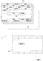
- the figure 3 illustrates an embodiment of a physical organization of data in a flash memory.
- the transition between logical organization ( figure 2 ) and the physical organization of the data storage is transparent to the processing unit 11 and the other circuits accessing the memory.
- the memory management unit 2 converts virtual addresses provided by the different entities into physical addresses. Moreover, to manage the atomicity, the management unit generates metadata which are also stored in the memory 2.
- the memory is physically organized into pages P, representing the erasure granularity.
- the memory is therefore divided into r pages P of identical sizes.
- Each page has the same number of words, constituting the writing (and reading) granularity.
- the pages are preferably divided into two categories.
- a first category comprises pages P1 divided into n frames Fj each comprising several data words (set DBj) and the same number of words FMDj frame metadata (from one to a few, for example two). For example, all frames have the same number of data words.
- Each page P1 further comprises a number m (a few to a few tens) of page metadata words PMD1 (k) independent of the frames.
- the number of data words of each frame preferably corresponds to an integer multiple (at least 1) of the number of data words of each DB block of the virtual organization of the memory.
- a frame Fj contains a DBj data block and FMDj frame metadata.
- FIG 3 we have illustrated, for each frame, the DBj block followed by FMDj metadata. However, preferably and as will be seen later, part of the metadata is written at the beginning of the frame Fj.
- a second category of pages in a much smaller number than the number of pages P1 of the first category, contains only memory metadata words MMDh.
- the second category has only one page Pr and the first category therefore comprises r-1 pages Pl.
- a page contains 1024 bytes. It is expected that r-1 pages P1 of the first category will each contain 25 frames of 10 words each and 6 words of page PMD1 metadata. Each frame Fj contains a DBj block, eight W words of data, and two FMDj frame metadata words. According to this particular embodiment, each frame can therefore contain two logical blocks Bi. Moreover, a single page Pr of MMDh words of memory metadata is provided.
- the FMDj frame metadata contain at least one word FCONST (preferably a single word FMDj (1)) of fixed value, identical regardless of the value of the data contained in the DBj block and at least one word (preferably a single word FMDj (2)) containing the number or numbers (identifier (s) i) of the virtual block (s) Bi written in the real block DBj.
- the word FMDj (2) also contains a status indicator FW (end of writing) of the DBj block and an error control code of CRC type, signature or other.
- the frame metadata is used for the frame atomicity, i.e. whether the DBj block contained in the frame is stable or not.
- the figure 4 illustrates, very schematically, an embodiment of a frame structure 4 Fj assuming two FMDj metadata words.
- the metadata word FMDj (1) of fixed value FCONST is first written, then the words of the data item A and finally the metadata word FMDj (2).
- the CRC code contained in the word FMDj (2) is preferably a CRC of the word FMDj (1) and the block DBj. Thanks to the use of a fixed value for the word FMDj (1), we will be able to ensure that there was no tearing or attack at the beginning of the writing of the frame, for example an attempt to modify the content of the DBj block during an attack.
- the value is fixed, that is to say the same for a given frame, but can vary from one frame to another. Preferably, for convenience, the value is the same for all the frames of the memory.
- the page metadata PMD1 contains a word PMD1 (1) indicating that the page has started to be written and that it is no longer blank, preferably but optionally a word PMD1 (2) indicating that the page is full, a word PMDl (3) indicating that the next page is erased (therefore blank), a word PMDl (4) indicating that the page is obsolete, that is to say that none of the frames contains a block still useful (in other words, that all the blocks of this page have already been modified in other pages previously) and a word PMDl (5) containing a sequence number of the page, that is, ie the value of a PWN counter of the number of pages written.
- the page metadata according to this first aspect is used to indicate the switchover from one page to another and to allow an atomicity recovery at start or reset of the circuit. The words are not necessarily physically in this order on the page.
- the page metadata furthermore contains, or instead of the word PMD1 (3) indicating that the page has been erased, a word PMD (6) indicating the number of erasures that has occurred. the page.
- the writing of the data in the memory is carried out block by block as and when they are received and successively in each page.
- this same block of data Bi can be found written several times in the memory with different values as and when writings. This contributes to the resolution of the atomicity problem insofar as, from the moment when a datum A has been written once with a first value, it will always be possible, when writing later, to return to the previous value representing the Steady state if there is a problem writing the current value.
- the same data A is always "stored" in the same block Bi (or the same blocks).
- the identifier i the address of the block Bi in the logical memory makes it possible to retrieve the physical block or blocks DBj of the memory 2 containing the data item A (containing the successive values of the data item A).
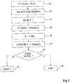
- the figure 5 is a block diagram illustrating an embodiment of a writing of a data item A in the memory 2.
- the page P1 having the highest number of PWN pages written is selected (block 52, SELECT l (MAX (PWN)) by browsing (reading) the corresponding words PMD1 (5) of the page metadata.
- the first frame Fj available sequentially in the page Pl. This selection is made, for example, by traversing the frames successively to the first whose word FMDj (1) intended at the fixed value FCONST is not programmed.
- the second word FMDj (2) of metadata is read and the first frame is selected whose flag FW at the end of writing FMDj is in the state 1 or whose block identifier i is not programmed. . It is assumed in this example that a new page is opened at the end of the writing of the last frame of a page. Therefore there is inevitably a frame available in step 53.
- the frame Fj starts by writing (block 54, FCONST -> FMDj (1)), in the frame Fj, the first word FMDj (1) fixed metadata (it is actually the first word written logically.Physically, the words can be in a different order in the frame). Then write (block 55, A -> DBj) the data A in the block DBj, then write (block 56, (i, FW, CRC) -> FMDj (2)) the second word FMDj (2) of metadata with the identifier i, the end indicator FW the CRC of the first words (FMDj (1) and DBj) of the frame.
- step 53 is returned to write in the next frame.
- the frames are of variable size and where the space available at the end of the page is not sufficient to store the following frame, either leave a blank space, or cut the frame in two and stores a portion on the current page and a portion on the next page.
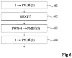
- the figure 6 is a block diagram illustrating an embodiment of a preparation of a next page for writing when a current page is full.
- the figure 7 illustrates, in block diagram form, an embodiment of a reading of a data item A in the memory 2.
- the reading in the memory is performed by browsing the frames Fj from the last written frame of the last page written by searching in which DBj block is the block Bi, by its identifier i.
- the status indicator FW which indicates whether the writing of the frame has ended without tearing indicating, in principle, whether the data are stable or not. no.
- the figure 8 is a block diagram illustrating an embodiment of a page-level atomic recovery.
- this process is performed at startup or during a reset of the circuit, which amounts to checking the atomicity after each accidental or voluntary tearing or extinguishing.
- the page Pr is then used to transfer (block 84, TRANSFER DBj (Pl) -> DBj '(Pr)) all the valid frames from the page Pl to the page Pr.
- the page P1 (block 85, ERASE P1) is deleted.
- the various steps of the copy, to the page Pr and then the copy from the page Pr, are validated by metadata words in the page Pr to ensure that in case of tearing during the recovery procedure, the procedure started is continued well and we do not start again at the beginning of the tearing procedure at the risk of permanently losing the still valid data in the page Pl.
- the page Pr is a dedicated page of the memory.
- An inverse transfer (block 86, TRANSFER DBj '(Pr) -> DBj (Pl)) of the data temporarily stored in the page Pr to the deleted page P1 is then carried out.
- the page metadata is then also rewritten.
- we delete the page Pr (block 87, ERASE Pr) so that it is ready for next use.
- the page Pr is any available page. In this case, it is not necessary to transfer the data to the Pl page after deletion.
- the treatment of figure 8 also includes a step of checking the atomicity of the page metadata. For this, it verifies, during a restart and on the last page written, an error correction code stored in one of the page metadata words PMDl (k).
- the PMD1 (2) metadata words of all the pages that are written after the selected frame Fj in block 82 are written as indicating a full page.
- these pages can not be used without being erased.
- the number of available pages (erased) is at least two in order to erase a page.
- one selects one of the written pages preferably the page whose number of written frames is minimum.
- This page is then scanned to be erased by checking its frames and those of them which contain the last reliable states of blocks Bi. All these blocks are transferred (written) in the manner described in relation to the figure 4 to one of the available pages.
- at most n blocks are transferred (in practice, there are at least some frames that contain obsolete data so that this transfer results in frames available in this page).
- the original page is erased. After erasing, the erased page indicator (PMD1 (4)) is programmed.
- a minimum number of upper pages for example three or four, is fixed so as to have more available frames in order to store a larger number of transactions without requiring an erasure.
- each erasing of a page of the flash memory 2 increments a number of erasure counter of the page concerned.
- the figure 9 is a block diagram illustrating an embodiment of a selection of a page to be erased according to this second aspect.
- the selection of the page to be erased does not necessarily correspond to the page having the minimum value of the number of pages written but to that having the minimum value of pages written among the pages having undergone a smaller number of erasures. .
- the application of this embodiment makes it possible to optimize the lifetime of the flash memory by optimizing the homogeneity of the number of erasures among the number of pages. Indeed, if there was no atomic recovery process, the page having the maximum value of the number of pages written would be among those having been erased a lesser number of times. However, since the application of the page-level atomic recovery process results in a transfer, with the same value of the number of pages written to an available page, this does not necessarily correspond, especially in case of many implementations of atomic recovery.
- this second aspect can be combined with the first, it can also be implemented more generally in any method of managing a flash memory.
- Another advantage is that in case of implementation of the process of atomic recovery at the level of a page as described in connection with the figure 9 , there is a risk that the error is in the number of pages written, in which case this page risk, without the implementation of the number of erasures counter, never to be erased.
- An advantage of the embodiments that have been described is that they improve the management of a flash memory for the processing of operations that must comply with an atomicity criterion.
- Another advantage is that they easily make it possible to go back to the last atomic value of a datum.
Landscapes
- Engineering & Computer Science (AREA)
- Theoretical Computer Science (AREA)
- General Engineering & Computer Science (AREA)
- Physics & Mathematics (AREA)
- General Physics & Mathematics (AREA)
- Human Computer Interaction (AREA)
- Computer Security & Cryptography (AREA)
- Quality & Reliability (AREA)
- Techniques For Improving Reliability Of Storages (AREA)
- Information Retrieval, Db Structures And Fs Structures Therefor (AREA)
Applications Claiming Priority (1)
| Application Number | Priority Date | Filing Date | Title |
|---|---|---|---|
| FR1654490A FR3051574A1 (fr) | 2016-05-20 | 2016-05-20 | Gestion du stockage dans une memoire flash |
Publications (1)
| Publication Number | Publication Date |
|---|---|
| EP3246820A1 true EP3246820A1 (de) | 2017-11-22 |
Family
ID=57184538
Family Applications (1)
| Application Number | Title | Priority Date | Filing Date |
|---|---|---|---|
| EP16198176.6A Withdrawn EP3246820A1 (de) | 2016-05-20 | 2016-11-10 | Verwaltung der speicherung in einem flash-speicher |
Country Status (4)
| Country | Link |
|---|---|
| US (1) | US10162540B2 (de) |
| EP (1) | EP3246820A1 (de) |
| CN (1) | CN107402717B (de) |
| FR (1) | FR3051574A1 (de) |
Families Citing this family (3)
| Publication number | Priority date | Publication date | Assignee | Title |
|---|---|---|---|---|
| FR3055992A1 (fr) * | 2016-09-09 | 2018-03-16 | Proton World International N.V. | Gestion d'index dans une memoire flash |
| FR3072476A1 (fr) | 2017-10-13 | 2019-04-19 | Proton World International N.V. | Unite logique de memoire pour memoire flash |
| CN112069004B (zh) * | 2020-08-21 | 2023-01-06 | 苏州浪潮智能科技有限公司 | 一种闪存芯片中块读取与页读取换算关系测试方法及系统 |
Citations (5)
| Publication number | Priority date | Publication date | Assignee | Title |
|---|---|---|---|---|
| US5457658A (en) * | 1993-02-24 | 1995-10-10 | International Business Machines Corporation | Nonvolatile memory with cluster-erase flash capability and solid state file apparatus using the same |
| US6513095B1 (en) * | 1999-05-31 | 2003-01-28 | Sharp Kabushiki Kaisha | File system with assured integrity incorporating semiconductor memory device |
| EP2058737A1 (de) * | 2007-11-06 | 2009-05-13 | Sony Corporation | Speichervorrichtung, Speicherverwaltungsverfahren und Programm |
| US20100169543A1 (en) * | 2008-12-31 | 2010-07-01 | Joseph Edgington | Recovery for non-volatile memory after power loss |
| WO2012013683A1 (en) * | 2010-07-28 | 2012-02-02 | Fujitsu Semiconductor Europe Gmbh | Electronic apparatuses |
Family Cites Families (10)
| Publication number | Priority date | Publication date | Assignee | Title |
|---|---|---|---|---|
| KR100644602B1 (ko) * | 2000-10-11 | 2006-11-10 | 삼성전자주식회사 | 플래시메모리를 위한 재사상 제어방법 및 그에 따른플래시 메모리의 구조 |
| JP4772214B2 (ja) * | 2001-06-08 | 2011-09-14 | ルネサスエレクトロニクス株式会社 | 不揮発性記憶装置及びその書き換え制御方法 |
| US7707480B2 (en) | 2005-07-01 | 2010-04-27 | Qnx Software Systems Gmbh & Co. Kg | System employing data verification operations of differing computational costs |
| US8195945B2 (en) * | 2005-12-01 | 2012-06-05 | Sony Mobile Communications Ab | Secure digital certificate storing scheme for flash memory and electronic apparatus |
| KR100922389B1 (ko) | 2007-07-04 | 2009-10-19 | 삼성전자주식회사 | 플래시 메모리를 위한 색인 스킴 |
| US7978516B2 (en) * | 2007-12-27 | 2011-07-12 | Pliant Technology, Inc. | Flash memory controller having reduced pinout |
| US8516219B2 (en) | 2009-07-24 | 2013-08-20 | Apple Inc. | Index cache tree |
| US8296496B2 (en) * | 2009-09-17 | 2012-10-23 | Hewlett-Packard Development Company, L.P. | Main memory with non-volatile memory and DRAM |
| US8812816B2 (en) | 2010-03-23 | 2014-08-19 | Apple Inc. | Garbage collection schemes for index block |
| KR102295223B1 (ko) * | 2015-01-13 | 2021-09-01 | 삼성전자주식회사 | 속도 모드 관리자를 포함하는 저장 장치 및 사용자 장치 |
-
2016
- 2016-05-20 FR FR1654490A patent/FR3051574A1/fr not_active Withdrawn
- 2016-11-10 EP EP16198176.6A patent/EP3246820A1/de not_active Withdrawn
- 2016-11-25 CN CN201611054274.4A patent/CN107402717B/zh active Active
- 2016-12-15 US US15/380,509 patent/US10162540B2/en active Active
Patent Citations (5)
| Publication number | Priority date | Publication date | Assignee | Title |
|---|---|---|---|---|
| US5457658A (en) * | 1993-02-24 | 1995-10-10 | International Business Machines Corporation | Nonvolatile memory with cluster-erase flash capability and solid state file apparatus using the same |
| US6513095B1 (en) * | 1999-05-31 | 2003-01-28 | Sharp Kabushiki Kaisha | File system with assured integrity incorporating semiconductor memory device |
| EP2058737A1 (de) * | 2007-11-06 | 2009-05-13 | Sony Corporation | Speichervorrichtung, Speicherverwaltungsverfahren und Programm |
| US20100169543A1 (en) * | 2008-12-31 | 2010-07-01 | Joseph Edgington | Recovery for non-volatile memory after power loss |
| WO2012013683A1 (en) * | 2010-07-28 | 2012-02-02 | Fujitsu Semiconductor Europe Gmbh | Electronic apparatuses |
Also Published As
| Publication number | Publication date |
|---|---|
| FR3051574A1 (fr) | 2017-11-24 |
| CN107402717A (zh) | 2017-11-28 |
| US10162540B2 (en) | 2018-12-25 |
| CN107402717B (zh) | 2020-09-04 |
| US20170336996A1 (en) | 2017-11-23 |
Similar Documents
| Publication | Publication Date | Title |
|---|---|---|
| EP1988548B1 (de) | Nicht flüchtiger Speicher mit Schnellschreiben | |
| EP0546048A1 (de) | Ein verfahren und eine vorrichtung für speicherung der information in einem speicher und ihre benutzung in speicherkarten. | |
| EP3293637A1 (de) | Indexverwaltung in einem flash-speicher | |
| EP2786317B1 (de) | Schreiben von daten in einen nichtflüchtigen speicher einer chipkarte | |
| EP0606029B1 (de) | IC Karte mit alterunggeschützten Daten und Programmen | |
| EP2940690B1 (de) | Bidirektionaler Zähler in einem Flash-Speicher | |
| EP0769742B1 (de) | Elektronisches Bauelement mit einem elektrisch löschbaren und nichtflüchtigen Speicher | |
| EP3246820A1 (de) | Verwaltung der speicherung in einem flash-speicher | |
| EP3246819B1 (de) | Zähler in einem flash-speicher | |
| FR2689662A1 (fr) | Procédé de protection d'une carte à puce contre la perte d'information. | |
| FR3051575A1 (fr) | Gestion de l'effacement dans une memoire flash | |
| EP3188024B1 (de) | Speicherung in einem flash-speicher | |
| FR3012655A1 (fr) | Compteur en memoire flash | |
| FR2830667A1 (fr) | Procede de determination d'une zone stable dans une memoire et dispositif de gestion d'une memoire associe | |
| FR2915828A1 (fr) | Memoire non volatile a secteurs auxiliaires tournants | |
| EP3188032B1 (de) | Datenspeicherung in einem flash-speicher | |
| EP3416087A1 (de) | Steuerung der atomarität in einem eeprom-speicher | |
| CA2452672A1 (fr) | Procede de modification des donnees d'une carte a memoire lors d'une transaction | |
| EP2339587A1 (de) | Löschsicherung eines Speichers vom Typ Flashprom | |
| FR2915829A1 (fr) | Memoire non volatile a ecriture rapide | |
| EP2339586A1 (de) | Verwaltungsverfahren von Daten | |
| WO2007077242A1 (fr) | Procede de gestion de donnees destinees a etre ecrites et lues dans une memoire |
Legal Events
| Date | Code | Title | Description |
|---|---|---|---|
| PUAI | Public reference made under article 153(3) epc to a published international application that has entered the european phase |
Free format text: ORIGINAL CODE: 0009012 |
|
| 17P | Request for examination filed |
Effective date: 20161110 |
|
| AK | Designated contracting states |
Kind code of ref document: A1 Designated state(s): AL AT BE BG CH CY CZ DE DK EE ES FI FR GB GR HR HU IE IS IT LI LT LU LV MC MK MT NL NO PL PT RO RS SE SI SK SM TR |
|
| AX | Request for extension of the european patent |
Extension state: BA ME |
|
| 17Q | First examination report despatched |
Effective date: 20180129 |
|
| STAA | Information on the status of an ep patent application or granted ep patent |
Free format text: STATUS: THE APPLICATION HAS BEEN WITHDRAWN |
|
| 18W | Application withdrawn |
Effective date: 20190904 |