EP3246907A1 - Substrat de réseau d'affichage, procédé de compensation, panneau d'affichage et dispositif d'affichage - Google Patents
Substrat de réseau d'affichage, procédé de compensation, panneau d'affichage et dispositif d'affichage Download PDFInfo
- Publication number
- EP3246907A1 EP3246907A1 EP15794046.1A EP15794046A EP3246907A1 EP 3246907 A1 EP3246907 A1 EP 3246907A1 EP 15794046 A EP15794046 A EP 15794046A EP 3246907 A1 EP3246907 A1 EP 3246907A1
- Authority
- EP
- European Patent Office
- Prior art keywords
- power supply
- supply voltage
- voltage input
- array substrate
- input points
- Prior art date
- Legal status (The legal status is an assumption and is not a legal conclusion. Google has not performed a legal analysis and makes no representation as to the accuracy of the status listed.)
- Withdrawn
Links
Images



Classifications
-
- G—PHYSICS
- G09—EDUCATION; CRYPTOGRAPHY; DISPLAY; ADVERTISING; SEALS
- G09G—ARRANGEMENTS OR CIRCUITS FOR CONTROL OF INDICATING DEVICES USING STATIC MEANS TO PRESENT VARIABLE INFORMATION
- G09G3/00—Control arrangements or circuits, of interest only in connection with visual indicators other than cathode-ray tubes
- G09G3/20—Control arrangements or circuits, of interest only in connection with visual indicators other than cathode-ray tubes for presentation of an assembly of a number of characters, e.g. a page, by composing the assembly by combination of individual elements arranged in a matrix no fixed position being assigned to or needed to be assigned to the individual characters or partial characters
- G09G3/22—Control arrangements or circuits, of interest only in connection with visual indicators other than cathode-ray tubes for presentation of an assembly of a number of characters, e.g. a page, by composing the assembly by combination of individual elements arranged in a matrix no fixed position being assigned to or needed to be assigned to the individual characters or partial characters using controlled light sources
- G09G3/30—Control arrangements or circuits, of interest only in connection with visual indicators other than cathode-ray tubes for presentation of an assembly of a number of characters, e.g. a page, by composing the assembly by combination of individual elements arranged in a matrix no fixed position being assigned to or needed to be assigned to the individual characters or partial characters using controlled light sources using electroluminescent panels
- G09G3/32—Control arrangements or circuits, of interest only in connection with visual indicators other than cathode-ray tubes for presentation of an assembly of a number of characters, e.g. a page, by composing the assembly by combination of individual elements arranged in a matrix no fixed position being assigned to or needed to be assigned to the individual characters or partial characters using controlled light sources using electroluminescent panels semiconductive, e.g. using light-emitting diodes [LED]
- G09G3/3208—Control arrangements or circuits, of interest only in connection with visual indicators other than cathode-ray tubes for presentation of an assembly of a number of characters, e.g. a page, by composing the assembly by combination of individual elements arranged in a matrix no fixed position being assigned to or needed to be assigned to the individual characters or partial characters using controlled light sources using electroluminescent panels semiconductive, e.g. using light-emitting diodes [LED] organic, e.g. using organic light-emitting diodes [OLED]
- G09G3/3225—Control arrangements or circuits, of interest only in connection with visual indicators other than cathode-ray tubes for presentation of an assembly of a number of characters, e.g. a page, by composing the assembly by combination of individual elements arranged in a matrix no fixed position being assigned to or needed to be assigned to the individual characters or partial characters using controlled light sources using electroluminescent panels semiconductive, e.g. using light-emitting diodes [LED] organic, e.g. using organic light-emitting diodes [OLED] using an active matrix
- G09G3/3233—Control arrangements or circuits, of interest only in connection with visual indicators other than cathode-ray tubes for presentation of an assembly of a number of characters, e.g. a page, by composing the assembly by combination of individual elements arranged in a matrix no fixed position being assigned to or needed to be assigned to the individual characters or partial characters using controlled light sources using electroluminescent panels semiconductive, e.g. using light-emitting diodes [LED] organic, e.g. using organic light-emitting diodes [OLED] using an active matrix with pixel circuitry controlling the current through the light-emitting element
-
- G—PHYSICS
- G06—COMPUTING OR CALCULATING; COUNTING
- G06F—ELECTRIC DIGITAL DATA PROCESSING
- G06F1/00—Details not covered by groups G06F3/00 - G06F13/00 and G06F21/00
- G06F1/26—Power supply means, e.g. regulation thereof
-
- G—PHYSICS
- G09—EDUCATION; CRYPTOGRAPHY; DISPLAY; ADVERTISING; SEALS
- G09G—ARRANGEMENTS OR CIRCUITS FOR CONTROL OF INDICATING DEVICES USING STATIC MEANS TO PRESENT VARIABLE INFORMATION
- G09G3/00—Control arrangements or circuits, of interest only in connection with visual indicators other than cathode-ray tubes
- G09G3/20—Control arrangements or circuits, of interest only in connection with visual indicators other than cathode-ray tubes for presentation of an assembly of a number of characters, e.g. a page, by composing the assembly by combination of individual elements arranged in a matrix no fixed position being assigned to or needed to be assigned to the individual characters or partial characters
- G09G3/22—Control arrangements or circuits, of interest only in connection with visual indicators other than cathode-ray tubes for presentation of an assembly of a number of characters, e.g. a page, by composing the assembly by combination of individual elements arranged in a matrix no fixed position being assigned to or needed to be assigned to the individual characters or partial characters using controlled light sources
- G09G3/30—Control arrangements or circuits, of interest only in connection with visual indicators other than cathode-ray tubes for presentation of an assembly of a number of characters, e.g. a page, by composing the assembly by combination of individual elements arranged in a matrix no fixed position being assigned to or needed to be assigned to the individual characters or partial characters using controlled light sources using electroluminescent panels
- G09G3/32—Control arrangements or circuits, of interest only in connection with visual indicators other than cathode-ray tubes for presentation of an assembly of a number of characters, e.g. a page, by composing the assembly by combination of individual elements arranged in a matrix no fixed position being assigned to or needed to be assigned to the individual characters or partial characters using controlled light sources using electroluminescent panels semiconductive, e.g. using light-emitting diodes [LED]
- G09G3/3208—Control arrangements or circuits, of interest only in connection with visual indicators other than cathode-ray tubes for presentation of an assembly of a number of characters, e.g. a page, by composing the assembly by combination of individual elements arranged in a matrix no fixed position being assigned to or needed to be assigned to the individual characters or partial characters using controlled light sources using electroluminescent panels semiconductive, e.g. using light-emitting diodes [LED] organic, e.g. using organic light-emitting diodes [OLED]
-
- G—PHYSICS
- G09—EDUCATION; CRYPTOGRAPHY; DISPLAY; ADVERTISING; SEALS
- G09G—ARRANGEMENTS OR CIRCUITS FOR CONTROL OF INDICATING DEVICES USING STATIC MEANS TO PRESENT VARIABLE INFORMATION
- G09G3/00—Control arrangements or circuits, of interest only in connection with visual indicators other than cathode-ray tubes
- G09G3/20—Control arrangements or circuits, of interest only in connection with visual indicators other than cathode-ray tubes for presentation of an assembly of a number of characters, e.g. a page, by composing the assembly by combination of individual elements arranged in a matrix no fixed position being assigned to or needed to be assigned to the individual characters or partial characters
- G09G3/22—Control arrangements or circuits, of interest only in connection with visual indicators other than cathode-ray tubes for presentation of an assembly of a number of characters, e.g. a page, by composing the assembly by combination of individual elements arranged in a matrix no fixed position being assigned to or needed to be assigned to the individual characters or partial characters using controlled light sources
- G09G3/30—Control arrangements or circuits, of interest only in connection with visual indicators other than cathode-ray tubes for presentation of an assembly of a number of characters, e.g. a page, by composing the assembly by combination of individual elements arranged in a matrix no fixed position being assigned to or needed to be assigned to the individual characters or partial characters using controlled light sources using electroluminescent panels
- G09G3/32—Control arrangements or circuits, of interest only in connection with visual indicators other than cathode-ray tubes for presentation of an assembly of a number of characters, e.g. a page, by composing the assembly by combination of individual elements arranged in a matrix no fixed position being assigned to or needed to be assigned to the individual characters or partial characters using controlled light sources using electroluminescent panels semiconductive, e.g. using light-emitting diodes [LED]
- G09G3/3208—Control arrangements or circuits, of interest only in connection with visual indicators other than cathode-ray tubes for presentation of an assembly of a number of characters, e.g. a page, by composing the assembly by combination of individual elements arranged in a matrix no fixed position being assigned to or needed to be assigned to the individual characters or partial characters using controlled light sources using electroluminescent panels semiconductive, e.g. using light-emitting diodes [LED] organic, e.g. using organic light-emitting diodes [OLED]
- G09G3/3225—Control arrangements or circuits, of interest only in connection with visual indicators other than cathode-ray tubes for presentation of an assembly of a number of characters, e.g. a page, by composing the assembly by combination of individual elements arranged in a matrix no fixed position being assigned to or needed to be assigned to the individual characters or partial characters using controlled light sources using electroluminescent panels semiconductive, e.g. using light-emitting diodes [LED] organic, e.g. using organic light-emitting diodes [OLED] using an active matrix
-
- G—PHYSICS
- G09—EDUCATION; CRYPTOGRAPHY; DISPLAY; ADVERTISING; SEALS
- G09G—ARRANGEMENTS OR CIRCUITS FOR CONTROL OF INDICATING DEVICES USING STATIC MEANS TO PRESENT VARIABLE INFORMATION
- G09G3/00—Control arrangements or circuits, of interest only in connection with visual indicators other than cathode-ray tubes
- G09G3/20—Control arrangements or circuits, of interest only in connection with visual indicators other than cathode-ray tubes for presentation of an assembly of a number of characters, e.g. a page, by composing the assembly by combination of individual elements arranged in a matrix no fixed position being assigned to or needed to be assigned to the individual characters or partial characters
- G09G3/22—Control arrangements or circuits, of interest only in connection with visual indicators other than cathode-ray tubes for presentation of an assembly of a number of characters, e.g. a page, by composing the assembly by combination of individual elements arranged in a matrix no fixed position being assigned to or needed to be assigned to the individual characters or partial characters using controlled light sources
- G09G3/30—Control arrangements or circuits, of interest only in connection with visual indicators other than cathode-ray tubes for presentation of an assembly of a number of characters, e.g. a page, by composing the assembly by combination of individual elements arranged in a matrix no fixed position being assigned to or needed to be assigned to the individual characters or partial characters using controlled light sources using electroluminescent panels
- G09G3/32—Control arrangements or circuits, of interest only in connection with visual indicators other than cathode-ray tubes for presentation of an assembly of a number of characters, e.g. a page, by composing the assembly by combination of individual elements arranged in a matrix no fixed position being assigned to or needed to be assigned to the individual characters or partial characters using controlled light sources using electroluminescent panels semiconductive, e.g. using light-emitting diodes [LED]
- G09G3/3208—Control arrangements or circuits, of interest only in connection with visual indicators other than cathode-ray tubes for presentation of an assembly of a number of characters, e.g. a page, by composing the assembly by combination of individual elements arranged in a matrix no fixed position being assigned to or needed to be assigned to the individual characters or partial characters using controlled light sources using electroluminescent panels semiconductive, e.g. using light-emitting diodes [LED] organic, e.g. using organic light-emitting diodes [OLED]
- G09G3/3225—Control arrangements or circuits, of interest only in connection with visual indicators other than cathode-ray tubes for presentation of an assembly of a number of characters, e.g. a page, by composing the assembly by combination of individual elements arranged in a matrix no fixed position being assigned to or needed to be assigned to the individual characters or partial characters using controlled light sources using electroluminescent panels semiconductive, e.g. using light-emitting diodes [LED] organic, e.g. using organic light-emitting diodes [OLED] using an active matrix
- G09G3/3258—Control arrangements or circuits, of interest only in connection with visual indicators other than cathode-ray tubes for presentation of an assembly of a number of characters, e.g. a page, by composing the assembly by combination of individual elements arranged in a matrix no fixed position being assigned to or needed to be assigned to the individual characters or partial characters using controlled light sources using electroluminescent panels semiconductive, e.g. using light-emitting diodes [LED] organic, e.g. using organic light-emitting diodes [OLED] using an active matrix with pixel circuitry controlling the voltage across the light-emitting element
-
- G—PHYSICS
- G09—EDUCATION; CRYPTOGRAPHY; DISPLAY; ADVERTISING; SEALS
- G09G—ARRANGEMENTS OR CIRCUITS FOR CONTROL OF INDICATING DEVICES USING STATIC MEANS TO PRESENT VARIABLE INFORMATION
- G09G2300/00—Aspects of the constitution of display devices
- G09G2300/04—Structural and physical details of display devices
- G09G2300/0421—Structural details of the set of electrodes
- G09G2300/0426—Layout of electrodes and connections
-
- G—PHYSICS
- G09—EDUCATION; CRYPTOGRAPHY; DISPLAY; ADVERTISING; SEALS
- G09G—ARRANGEMENTS OR CIRCUITS FOR CONTROL OF INDICATING DEVICES USING STATIC MEANS TO PRESENT VARIABLE INFORMATION
- G09G2300/00—Aspects of the constitution of display devices
- G09G2300/08—Active matrix structure, i.e. with use of active elements, inclusive of non-linear two terminal elements, in the pixels together with light emitting or modulating elements
- G09G2300/0809—Several active elements per pixel in active matrix panels
- G09G2300/0842—Several active elements per pixel in active matrix panels forming a memory circuit, e.g. a dynamic memory with one capacitor
-
- G—PHYSICS
- G09—EDUCATION; CRYPTOGRAPHY; DISPLAY; ADVERTISING; SEALS
- G09G—ARRANGEMENTS OR CIRCUITS FOR CONTROL OF INDICATING DEVICES USING STATIC MEANS TO PRESENT VARIABLE INFORMATION
- G09G2320/00—Control of display operating conditions
- G09G2320/02—Improving the quality of display appearance
- G09G2320/0204—Compensation of DC component across the pixels in flat panels
-
- G—PHYSICS
- G09—EDUCATION; CRYPTOGRAPHY; DISPLAY; ADVERTISING; SEALS
- G09G—ARRANGEMENTS OR CIRCUITS FOR CONTROL OF INDICATING DEVICES USING STATIC MEANS TO PRESENT VARIABLE INFORMATION
- G09G2320/00—Control of display operating conditions
- G09G2320/02—Improving the quality of display appearance
- G09G2320/0233—Improving the luminance or brightness uniformity across the screen
-
- G—PHYSICS
- G09—EDUCATION; CRYPTOGRAPHY; DISPLAY; ADVERTISING; SEALS
- G09G—ARRANGEMENTS OR CIRCUITS FOR CONTROL OF INDICATING DEVICES USING STATIC MEANS TO PRESENT VARIABLE INFORMATION
- G09G2320/00—Control of display operating conditions
- G09G2320/02—Improving the quality of display appearance
- G09G2320/0242—Compensation of deficiencies in the appearance of colours
-
- G—PHYSICS
- G09—EDUCATION; CRYPTOGRAPHY; DISPLAY; ADVERTISING; SEALS
- G09G—ARRANGEMENTS OR CIRCUITS FOR CONTROL OF INDICATING DEVICES USING STATIC MEANS TO PRESENT VARIABLE INFORMATION
- G09G2330/00—Aspects of power supply; Aspects of display protection and defect management
- G09G2330/02—Details of power systems and of start or stop of display operation
- G09G2330/028—Generation of voltages supplied to electrode drivers in a matrix display other than LCD
Definitions
- the present disclosure relates to the field of an organic light-emitting diode (OLED) display technology, in particular to a display array substrate, a compensation method, a display panel and a display device.
- OLED organic light-emitting diode
- AMOLED Active matrix/organic light-emitting diode
- the OLED has such advantages as low power consumption, low production cost, self-luminescence, wide viewing angle and rapid response.
- the design of a pixel driving circuit is of an important significance.
- a stable current is required so as to control the OLED to emit light.
- an existing typical AMOLED pixel driving circuit includes one driving transistor DTFT, one switching transistor T1 and one storage capacitor Cs.
- a scanning signal Gate(n) on this row is of a low level, T1 is turned on, and a data voltage Vdata corresponding a grayscale level is written into the storage capacitor Cs.
- Gate(n) is changed to be of a high level, T1 is turned off, and DTFT is driven by a gate voltage stored in Cs, so that a current is generated by DTFT to drive the OLED, thereby to ensure the OLED to emit light continuously within one frame.
- An existing pixel compensation circuit merely compensates for the drift of the threshold voltage V th of DTFT in each pixel generated due to the manufacture process and the aging of elements.
- the current is also affected by the power supply voltage ELVDD.
- the OLED is a current-driven element, there is a relatively large current flowing through a power line for applying the power supply voltage ELVDD.
- the pixels in each column within an effective display region are connected to a corresponding power line, and the power supply voltage is applied by a power supply lead ELVDD_O located outside the effective display region to the power lines within the effective display region.
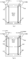
- the power supply voltage ELVDD at an upper left portion is larger than that at a middle left portion, and the power supply voltage ELVDD at the middle left portion is larger than that at a bottom left portion.
- the power supply voltage ELVDD at an upper right portion is larger than that at a middle right portion, and the power supply voltage ELVDD at the middle right portion is larger than that at a bottom right portion.
- a first power supply voltage input point BLP is located on the OLED display panel at the bottom left
- a second power supply voltage input point ULP is located on the OLED display panel at the upper left
- a third power supply voltage input point URP is located on the OLED display panel at the upper right
- a fourth power supply voltage input point BRP is located on the OLED display panel at the bottom right
- a fifth power supply voltage input point MLP is located on the OLED display panel at the middle left
- a sixth power supply voltage input point MRP is located on the OLED display panel at the middle right.
- the brightness of the entire OLED display panel gradually increases from top down, i.e., the brightness unevenness occurs.
- an appropriate material is selected so as to reduce a resistance of the power line for applying the ELVDD, thereby to reduce a difference in an IR drop (which refers to a voltage drop or rise across a network in an existing integrated circuit (IC) between the power supply and the ground).
- an IR drop which refers to a voltage drop or rise across a network in an existing integrated circuit (IC) between the power supply and the ground.
- Amain object of the present disclosure is to provide a display array substrate, a compensation method, a display panel and a display device, so as to prevent a difference in currents flowing through a driving transistor of a light-emitting element due to a difference in power supply voltages applied to pixels, thereby to prevent a difference in brightness of the pixels on the display panel.
- the present disclosure provides in one embodiment a display array substrate including at least one power line and a voltage application unit.
- the at least one power line is connected to pixels in at least one column within an effective display region on the display array substrate.
- the power application unit is arranged outside the effective display region and configured to apply power supply voltages to at least two power supply voltage input points on the at least one power line.
- An absolute value of a voltage difference between the at least two power supply voltage input points is less than a predetermined voltage threshold.
- the pixels in each column within the effective display region are connected to a corresponding power line, and the voltage application unit is configured to apply the power supply voltages to at least two power supply voltage input points on each power line on the display array substrate.
- the two power supply voltage input points are located at the top and the bottom of the power line, respectively.
- the three power supply voltage input points are located at the top, the middle and the bottom of the power line, respectively.
- the voltage difference between the at least two power supply voltage input points is zero.
- the voltage application unit includes a direct current (DC)/DC converter and a DC voltage source configured to generate a DC voltage.
- An input end of the DC/DC converter is configured to receive the DC voltage.
- the DC/DC converter includes at least two output ends corresponding to the at least two power supply voltage input points, respectively, and it is configured to generate a corresponding power supply voltage in accordance with an impedance between each output end and the corresponding power supply voltage input point, and apply the power supply voltage through the output end to the corresponding power supply voltage input point.
- the DC/DC converter includes at least two DC/DC conversion units corresponding to the at least two power supply voltage input points, respectively.
- the DC/DC conversion unit includes a low drop-out regulator (LDO), a positive phase input end of which is configured to receive the DC voltage, a negative phase input end of which is connected to an output end of the low drop-out regulator through a first divider resistor and grounded through a second divider resistor, and an output end of which is connected to the corresponding power supply voltage input point.
- LDO low drop-out regulator
- the voltage application unit includes at least two variable resistors corresponding to the at least two power supply voltage input points, respectively, and a DC voltage source for generating a DC voltage.
- a first end of the variable resistor is configured to receive the DC voltage, and a second end of the variable resistor is connected to the corresponding power supply voltage input point.
- the voltage application unit is further configured to apply the power supply voltages to the at least two power supply voltage input points on the power line via at least two external power supply leads within a wiring region on the display array substrate.
- the power supply voltage is applied to the power supply voltage input points on at least partial of different power lines via an identical external power supply lead.
- the display array substrate is an OLED array substrate.
- the present disclosure provides in one embodiment a compensation method for a display array substrate, including steps of : enabling pixels in at least one column within an effective display region on the display array substrate to be connected to at least one power line; selecting at least two power supply voltage input points on the at least one power line on the display array substrate; and applying power supply voltages to the at least two power supply voltage input points, an absolute value of a voltage difference between the at least two power supply voltage input points being less than a predetermined voltage threshold.
- the two power supply voltage input points are located at the top and the bottom of the power line, respectively.
- the three power supply voltage input points are located at the top, the middle and the bottom of the power line, respectively.
- the voltage difference between the at least two power supply voltage input points is zero.
- the power supply voltages are applied to the at least two power supply voltage input points on the power line via at least two external power supply leads, respectively.
- the step of applying the power supply voltages to the at least two power supply voltage input points includes: applying the power supply voltages to the at least two power supply voltage input points on each power line on the display array substrate.
- the power supply voltage is applied to the power supply voltage input points on at least partial of different power lines via an identical external power supply lead.
- the present disclosure provides in one embodiment a display panel including the above-mentioned display array substrate.
- the present disclosure provides in one embodiment a display device including the above-mentioned display array substrate or display panel.
- the power supply voltages are applied by the voltage application unit arranged outside the effective display region of the display array substrate to the at least two power supply voltage input points on the at least one power line on the display array substrate, and the absolute value of the voltage difference between the at least two power supply voltage input points is less than the predetermined voltage threshold.
- the present disclosure provides in one embodiment a display array substrate which includes at least one power line and a voltage application unit.
- the at least one power line is connected to pixels in at least one column within an effective display region on the display array substrate.
- the power application unit is arranged outside the effective display region and configured to apply power supply voltages to at least two power supply voltage input points on the at least power line.
- An absolute value of a voltage difference between the at least two power supply voltage input point is less than a predetermined voltage threshold.
- the voltage difference between the at least two power supply voltage input points is zero.
- the power supply voltages are applied by the voltage application unit arranged outside the effective display region of the display array substrate to the at least two power supply voltage input points on the at least one power line on the display array substrate, and the absolute value of the voltage difference between the at least two power supply voltage input points is less than the predetermined voltage threshold.
- the pixels in each column within the effective display region are connected to a power line, and the voltage application unit is configured to apply the power supply voltages to at least two power supply voltage input points on each power line on the display array substrate. In this way, it is able to prevent the brightness difference for the pixels in each column on the display array substrate.
- the two power supply voltage input points are located at the top and the bottom of the power line, respectively.
- the three power supply voltage input points are located at the top, the middle and the bottom of the power line, respectively.
- the voltage application unit is further configured to apply the power supply voltages to the at least two power supply voltage input points on the power line via at least two external power supply leads within a wiring region on the display array substrate.
- the voltage application unit is further configured to apply the power supply voltages to the at least two power supply voltage input points on the power line via at least two external power supply leads within a wiring region on the display array substrate.
- the power supply voltages are applied by the voltage application unit (not shown) located outside the effective display region of the display array substrate to a first power supply voltage input point BLP, a second power supply voltage input point ULP, a third power supply voltage input point URP and a fourth power supply voltage input point BRP via a first external power supply lead ELVDDBL, a second external power supply lead ELVDDUL, a third external power supply lead ELVDDUR and a fourth external power supply lead ELVDDBR, respectively.
- the first power supply voltage input point BLP is located at the bottom left of the display array substrate
- the second power supply voltage input point ULP is located at the upper left of the display array substrate
- the third power supply voltage input point URP is located at the upper right of the display array substrate
- the fourth power supply voltage input point BRP is located at the bottom right of the display array substrate.
- the entire display array substrate is divided into two portions, i.e., a left portion and a right portion.
- two power supply voltage input points are selected from each power line, they may be located at the top and bottom of the power line, respectively.
- the power lines at the left portion correspond to the first power supply voltage input point BLP and the second power supply voltage input point ULP
- the power lines at the right portion correspond to the third power supply voltage input point URP and the fourth power supply voltage input point BRP.
- the power supply voltage is applied to BLP via ELVDDBL
- the power supply voltage is applied to ULP via ELVDDUL
- the power supply voltage is applied to URP via ELVDDUR
- the power supply voltage is applied to BRP via ELVDDBR.
- the voltage difference between BLP and ULP is just a difference between voltage drops on ELVDDUL and ELVDDBL.
- ELVDDBL ELVDDUL+ ⁇ VL, wherein ⁇ VL represents a voltage drop on the ELVDDBL, so the voltage applied to BLP is identical to that applied to ULP.
- ELVDDBR ELVDDUR+ ⁇ VR, wherein ⁇ VR represents a voltage drop on the ELVDDBR, so the voltage applied to BRP is identical to that applied to URP.
- resistances of the external power supply leads need to be as small as possible, so as to reduce the voltage drops on the two or more external power supply leads, reduce the voltage difference between the power supply voltage input points and reduce the desired maximum power supply voltage, thereby to reduce the power consumption.
- the power supply voltage is applied to the power supply voltage input points on at least partial of different power lines via an identical external power supply lead.
- the power supply voltage may be applied to the second power supply voltage input point ULP at the upper left of the display array substrate and the third power supply voltage input point URP at the upper right of the display array substrate via an identical power supply lead, and/or the power supply voltage may be applied to the first power supply voltage input point BLP at the bottom left of the display array substrate and the fourth power supply voltage input point BRP at the bottom right of the display array substrate via an identical power line.
- the power supply voltage input points at an identical level at the left and right portions of the display array substrate may be connected to an identical power supply lead, so as to simplify the wiring.
- the power supply voltage may be also applied to the power supply voltage input points ULPs on the power lines at the left portion via an identical power supply lead ELVDDUL, and the power supply voltage may also be applied to the power supply voltage input points URPs on the power lines at the right portion via an identical power supply lead EVLDDUR.
- the power supply voltage is applied to the power supply voltage input points on different power lines via an identical external power supply lead, so as to simply the wiring.
- two additional power supply voltage input points are provided, i.e., a fifth power supply voltage input point MLP located at the middle left of the display array substrate, and a sixth power supply voltage input point MRP located at the middle right of the display array substrate.
- the voltage application unit includes a DC/DC converter and a DC voltage source configured to generate a DC voltage.
- An input end of the DC/DC converter is configured to receive the DC voltage.
- the DC/DC converter includes at least two output ends corresponding to the at least two power supply voltage input points, respectively, and it is configured to generate a corresponding power supply voltage in accordance with an impedance between each output end and the corresponding power supply voltage input point, and apply the power supply voltage through the output end to the corresponding power supply voltage input point.
- the voltage application unit includes a DC voltage source 21 for generating a DC voltage ELVDD and a DC/DC converter 22.
- An input end of the DC/DC converter 22 is configured to receive the DC voltage ELVDD generated by the DC voltage source 21.
- a DC voltage output end of the DC voltage source is connected to a grounded end GND via a first capacitor C1, so as to be insulated from an alternating current (AC) voltage.
- AC alternating current
- the DC/DC converter 22 includes a first output end BL corresponding to the first power supply voltage input point BLP, a second output end UL corresponding to the second power supply voltage input point ULP, a third output end UR corresponding to the third power supply voltage input point URP, and a fourth output end BR corresponding to the fourth power supply voltage input point BRP.
- the DC/DC converter 22 is configured to generate a first power supply voltage in accordance with an impedance between the first output end BL and the first power supply voltage input point BLP, and apply the first power supply voltage to the first power supply voltage input point BLP through the first output end BL and the first external power supply lead ELVDDBL; generate a second power supply voltage in accordance with an impedance between the second output end UL and the second power supply voltage input point ULP, and apply the second power supply voltage to the second power supply voltage input point ULP through the second output end UL and the second external power supply lead ELVDDUL; generate a third power supply voltage in accordance with an impedance between the third output end UR and the third power supply voltage input point URP, and apply the third power supply voltage to the third power supply voltage input point URP through the third output end UR and the third external power supply lead ELVDDUR; and generate a fourth power supply voltage in accordance with an impedance between the fourth output end BR and the fourth power supply voltage input point BRP, and apply the fourth
- the DC voltage ELVDD generated by the DV voltage source 21 is 0.1 V greater than a maximum one of a voltage at the first output end BL, a voltage at the second output end UL, a voltage at the third output end UR and a voltage at the fourth output end BR.
- the DC/DC converter may include four efficient bucking circuits, and meanwhile it is able for each circuit to adjust its output voltage.
- the DC/DC converter includes at least two DC/DC conversion units corresponding to the at least two power supply voltage input points, respectively.
- the DC/DC conversion unit includes a low drop-out regulator (LDO), a positive phase input end of which is configured to receive the DC voltage, a negative phase input end of which is connected to an output end of the low drop-out regulator through a first divider resistor and grounded through a second divider resistor, and the output end of which is connected to the corresponding power supply voltage input point.
- LDO low drop-out regulator
- the DC/DC converter may include a first DC/DC conversion unit, a second DC/DC conversion unit, a third DC/DC conversion unit and a fourth DC/DC conversion unit.
- the first DC/DC conversion unit includes a first LDO 31, a first resistor R1 and a second resistor R2.
- a positive phase input end of the first LDO 31 is configured to receive the DC voltage ELVDD, and a negative phase input end thereof is connected to an output end of the LDO 31 via the first resistor R1 and connected to the grounded end GND via the second resistor R2.
- the output end of the first LDO 31 serves as the first output end BL of the DC/DC converter 22 and is connected to the grounded end GND via a second capacitor C2.
- the second DC/DC conversion unit includes a second LDO 32, a third resistor R3 and a fourth resistor R4.
- a positive phase input end of the second LDO 32 is configured to receive the DC voltage ELVDD, and a negative phase input end thereof is connected to an output end of the second LDO 32 via the third resistor R3 and connected to the grounded end GND via the fourth resistor R4.
- the output end of the second LDO 32 serves as the second output end UL of the DC/.DC converter 22 and is connected to the grounded end GND via a third capacitor C3.
- the third DC/DC conversion unit includes a third LDO 33, a fifth resistor R5 and a sixth resistor R6.
- a positive phase input end of the third LDO 33 is configured to receive the DC voltage ELVDD, and a negative phase input end thereof is connected to an output end of the third LDO 33 via the fifth resistor R5 and connected to the grounded end GND via the sixth resistor R6.
- the output end of the third LDO 33 serves as the third output end UR of the DC/DC converter 22 and is connected to the grounded end GND via a fourth capacitor C4.
- the fourth DC/DC conversion unit includes a fourth LDO 34, a seventh resistor R7 and an eighth resistor R8.
- a positive phase input end of the fourth LDO 34 is configured to receive the DC voltage ELVDD, and a negative phase input end thereof is connected to an output end of the fourth LDO 34 via the seventh resistor R7 and connected to the grounded end GND via the eighth resistor R8.
- the output end of the fourth LDO 34 serves as the fourth output end BR of the DC/DC converter 22 and is connected to the grounded end GND via a fifth capacitor C5.
- resistances of R1, R3, R5 and R7 may be adjusted so as to enable the voltages applied to the four power supply voltage input points of the display array substrate (i.e., the first power supply voltage input point BLP at the bottom left of the display array substrate, the second power supply voltage input point ULP at the upper left of the display array substrate, the third power supply voltage input point URP at the upper right of the display array substrate, and the fourth power supply voltage input point BRP at the bottom right of the display array substrate) to be identical or similar to each other.
- the voltage application unit includes at least two variable resistors corresponding to the at least two power supply voltage input points, respectively, and a DC voltage source for generating a DC voltage.
- a first end of the variable resistor is configured to receive the DC voltage, and a second end of the variable resistor is connected to the corresponding power supply voltage input point.
- the voltage application unit includes a DC voltage source 21 for generating the DC voltage ELVDD, a first variable resistor RBL, a second variable resistor RUL, a third variable resistor RUR and a fourth variable resistor RBR.
- a first end of the first variable resistor RBL is configured to receive the DC voltage ELVDD, and a second end thereof, as the first output end BL of the DC/DC converter 22, is connected to the first power supply voltage input point.
- a first end of the second variable resistor RUL is configured to receive the DC voltage ELVDD, and a second end thereof, as the second output end UL of the DC/DC converter 22, is connected to the second power supply voltage input point.
- a first end of the third variable resistor RUR is configured to receive the DC voltage ELVDD, and a second end thereof, as the third output end UR of the DC/DC converter 22, is connected to the third power supply voltage input point.
- a first end of the fourth variable resistor RBR is configured to receive the DC voltage ELVDD, and a second end thereof, as the fourth output end BR of the DC/DC converter 22, is connected to the fourth power supply voltage input point.
- resistances of the first variable resistor RBL, the second variable resistor RUL, the third variable resistor RUR and the fourth variable resistor RBR may be adjusted so as to enable the voltages applied to the four power supply voltage input points of the display array substrate (i.e., the first power supply voltage input point BLP at the bottom left of the display array substrate, the second power supply voltage input point ULP at the upper left of the display array substrate, the third power supply voltage input point URP at the upper right of the display array substrate, and the fourth power supply voltage input point BRP at the bottom right of the display array substrate) to be identical or similar to each other.
- the four power supply voltage input points of the display array substrate i.e., the first power supply voltage input point BLP at the bottom left of the display array substrate, the second power supply voltage input point ULP at the upper left of the display array substrate, the third power supply voltage input point URP at the upper right of the display array substrate, and the fourth power supply voltage input point BRP at the bottom right of the display array substrate
- the display array substrate may be a liquid crystal array substrate, an OLED array substrate or any other display array substrate.
- the display array substrate is an OLED array substrate, so as to compensate for the IR voltage drop in a better manner.
- the present disclosure further provides in one embodiment a compensation method for a display array substrate, which includes steps of: enabling pixels in at least one column within an effective display region on the display array substrate to be connected to at least one power line; selecting at least two power supply voltage input points on the at least one power line on the display array substrate; and applying power supply voltages to the at least two power supply voltage input points, an absolute value of a voltage difference between the at least two power supply voltage input points being less than a predetermined voltage threshold.
- the two power supply voltage input points are located at the top and the bottom of the power line, respectively.
- the three power supply voltage input points are located at the top, the middle and the bottom of the power line, respectively.
- the voltage difference between the at least two power supply voltage input points is zero.
- the power supply voltages are applied to the at least two power supply voltage input points on the power line via at least two external power supply leads, respectively.
- the step of applying the power supply voltages to the at least two power supply voltage input points includes: applying the power supply voltages to the at least two power supply voltage input points on each power line on the display array substrate.
- the power supply voltage is applied to the power supply voltage input points on different power lines via an identical external power supply lead.
- the present disclosure further provides in one embodiment a display panel including the above-mentioned display array substrate.
- the present disclosure further provides in one embodiment a display device including the above-mentioned display array substrate or display panel.
- the display device may be a liquid crystal display device or an OLED display device, e.g., a liquid crystal TV, a mobile phone, a liquid crystal display or an OLED display.
- the display device is an OLED display, so as to compensate for the IR voltage drop in a better manner.
Landscapes
- Engineering & Computer Science (AREA)
- Theoretical Computer Science (AREA)
- Physics & Mathematics (AREA)
- General Physics & Mathematics (AREA)
- Computer Hardware Design (AREA)
- General Engineering & Computer Science (AREA)
- Electroluminescent Light Sources (AREA)
- Control Of Indicators Other Than Cathode Ray Tubes (AREA)
Applications Claiming Priority (2)
| Application Number | Priority Date | Filing Date | Title |
|---|---|---|---|
| CN201410796084.4A CN104409046A (zh) | 2014-12-18 | 2014-12-18 | 显示阵列基板、补偿方法、显示面板和显示装置 |
| PCT/CN2015/078740 WO2016095414A1 (fr) | 2014-12-18 | 2015-05-12 | Substrat de réseau d'affichage, procédé de compensation, panneau d'affichage et dispositif d'affichage |
Publications (2)
| Publication Number | Publication Date |
|---|---|
| EP3246907A1 true EP3246907A1 (fr) | 2017-11-22 |
| EP3246907A4 EP3246907A4 (fr) | 2018-08-01 |
Family
ID=52646670
Family Applications (1)
| Application Number | Title | Priority Date | Filing Date |
|---|---|---|---|
| EP15794046.1A Withdrawn EP3246907A4 (fr) | 2014-12-18 | 2015-05-12 | Substrat de réseau d'affichage, procédé de compensation, panneau d'affichage et dispositif d'affichage |
Country Status (4)
| Country | Link |
|---|---|
| US (1) | US9911382B2 (fr) |
| EP (1) | EP3246907A4 (fr) |
| CN (1) | CN104409046A (fr) |
| WO (1) | WO2016095414A1 (fr) |
Families Citing this family (19)
| Publication number | Priority date | Publication date | Assignee | Title |
|---|---|---|---|---|
| CN104409046A (zh) * | 2014-12-18 | 2015-03-11 | 京东方科技集团股份有限公司 | 显示阵列基板、补偿方法、显示面板和显示装置 |
| KR102356434B1 (ko) * | 2015-02-09 | 2022-01-28 | 삼성디스플레이 주식회사 | 유기발광 표시패널 |
| CN105206214A (zh) * | 2015-09-18 | 2015-12-30 | 京东方科技集团股份有限公司 | 显示电压供应装置、上电时序调节系统、方法和显示装置 |
| CN106448562A (zh) * | 2016-10-21 | 2017-02-22 | 京东方科技集团股份有限公司 | 显示面板及显示设备 |
| CN106409232A (zh) * | 2016-10-31 | 2017-02-15 | 昆山国显光电有限公司 | 补偿电压确定方法、装置、补偿方法、系统及驱动芯片 |
| KR102594393B1 (ko) * | 2016-12-21 | 2023-10-27 | 엘지디스플레이 주식회사 | 유기발광표시패널, 유기발광표시장치 |
| KR102516058B1 (ko) * | 2018-08-17 | 2023-03-31 | 삼성디스플레이 주식회사 | 표시 패널 |
| CN119942966A (zh) * | 2018-12-12 | 2025-05-06 | 群创光电股份有限公司 | 电子装置 |
| US11545542B2 (en) | 2019-01-22 | 2023-01-03 | Chengdu Boe Optoelectronics Technology Co., Ltd. | Display panel, display device, and method for manufacturing display panel |
| CN109872688B (zh) * | 2019-03-14 | 2021-01-26 | 京东方科技集团股份有限公司 | 电致发光显示面板和电致发光显示装置 |
| CN110310598B (zh) * | 2019-06-28 | 2021-05-28 | 上海天马有机发光显示技术有限公司 | 一种显示面板及其使用方法 |
| CN110634441A (zh) * | 2019-08-28 | 2019-12-31 | 武汉华星光电半导体显示技术有限公司 | Oled显示面板 |
| CN110648632B (zh) | 2019-09-30 | 2020-12-08 | 京东方科技集团股份有限公司 | 一种显示基板及其驱动方法 |
| CN110728921B (zh) * | 2019-10-31 | 2022-01-07 | Oppo广东移动通信有限公司 | 显示装置及电子设备 |
| US11756478B2 (en) | 2021-05-11 | 2023-09-12 | Tcl China Star Optoelectronics Technology Co., Ltd. | Driving circuit, display panel, and panel |
| CN113257175B (zh) * | 2021-05-11 | 2022-11-08 | Tcl华星光电技术有限公司 | 驱动电路、显示面板及面板 |
| US20230011187A1 (en) * | 2021-07-09 | 2023-01-12 | Meta Platforms Technologies, Llc | Dynamic compensation of power supply voltages for different sections of display area |
| CN116092428B (zh) * | 2023-01-28 | 2025-09-19 | 京东方科技集团股份有限公司 | 显示模组、显示装置及车载系统 |
| US20250358912A1 (en) * | 2024-05-15 | 2025-11-20 | Microsoft Technology Licensing, Llc | Mini-led display dcdc conversion allocation |
Family Cites Families (22)
| Publication number | Priority date | Publication date | Assignee | Title |
|---|---|---|---|---|
| JP4593740B2 (ja) | 2000-07-28 | 2010-12-08 | ルネサスエレクトロニクス株式会社 | 表示装置 |
| WO2005004096A1 (fr) * | 2003-07-08 | 2005-01-13 | Semiconductor Energy Laboratory Co., Ltd. | Systeme d'affichage et procede pour le commander |
| KR100589376B1 (ko) * | 2003-11-27 | 2006-06-14 | 삼성에스디아이 주식회사 | 역다중화기를 이용한 발광 표시 장치 |
| US7777738B2 (en) * | 2004-03-10 | 2010-08-17 | Koninklijke Philips Electronics N.V. | Active matrix display with reduction of power consumption |
| KR100729060B1 (ko) * | 2005-03-31 | 2007-06-14 | 삼성에스디아이 주식회사 | 발광 표시장치 및 그의 구동방법 |
| JP2007232795A (ja) | 2006-02-27 | 2007-09-13 | Hitachi Displays Ltd | 有機el表示装置 |
| KR20080090879A (ko) * | 2007-04-06 | 2008-10-09 | 삼성에스디아이 주식회사 | 유기 전계 발광 표시 장치 및 그 구동 방법 |
| US8120261B2 (en) * | 2007-12-04 | 2012-02-21 | Samsung Mobile Display Co., Ltd. | Organic electroluminescence display and driving method thereof |
| KR101246769B1 (ko) * | 2008-03-31 | 2013-03-26 | 샤프 가부시키가이샤 | 면 발광 표시장치 |
| KR101107161B1 (ko) * | 2009-08-18 | 2012-01-25 | 삼성모바일디스플레이주식회사 | 전원 공급 장치, 이를 포함하는 표시 장치 및 그 구동 방법 |
| KR101113451B1 (ko) * | 2009-12-01 | 2012-02-29 | 삼성모바일디스플레이주식회사 | 유기 전계발광 표시장치 |
| KR101155898B1 (ko) * | 2010-05-12 | 2012-06-20 | 삼성모바일디스플레이주식회사 | 유기발광 표시장치 및 그 구동 방법 |
| KR101156446B1 (ko) * | 2010-06-04 | 2012-06-18 | 삼성모바일디스플레이주식회사 | 유기 전계 발광 표시 장치 및 그 구동 방법 |
| KR20120001470A (ko) * | 2010-06-29 | 2012-01-04 | 삼성모바일디스플레이주식회사 | 전원 공급 장치, 이를 포함하는 표시 장치 및 그 구동 방법 |
| KR101323493B1 (ko) * | 2010-12-22 | 2013-10-31 | 엘지디스플레이 주식회사 | 유기발광다이오드 표시소자 |
| CN202166908U (zh) * | 2011-07-20 | 2012-03-14 | 天津瑞发科半导体技术有限公司 | 低压差线性稳压器与直流-直流转换器结合结构 |
| TW201340784A (zh) * | 2012-03-23 | 2013-10-01 | Ampower Technology Co Ltd | 發光二極體驅動系統及方法 |
| CN103927968B (zh) * | 2013-06-18 | 2016-12-28 | 上海天马微电子有限公司 | 一种oled显示装置 |
| KR102242214B1 (ko) * | 2014-03-05 | 2021-04-21 | 삼성디스플레이 주식회사 | 표시 장치 및 그 제조 방법 |
| CN104050915B (zh) * | 2014-05-30 | 2015-06-03 | 京东方科技集团股份有限公司 | Amoled显示面板和amoled显示装置 |
| CN204257177U (zh) * | 2014-12-18 | 2015-04-08 | 京东方科技集团股份有限公司 | 显示阵列基板、显示面板和显示装置 |
| CN104409046A (zh) | 2014-12-18 | 2015-03-11 | 京东方科技集团股份有限公司 | 显示阵列基板、补偿方法、显示面板和显示装置 |
-
2014
- 2014-12-18 CN CN201410796084.4A patent/CN104409046A/zh active Pending
-
2015
- 2015-05-12 EP EP15794046.1A patent/EP3246907A4/fr not_active Withdrawn
- 2015-05-12 WO PCT/CN2015/078740 patent/WO2016095414A1/fr not_active Ceased
- 2015-05-12 US US14/893,777 patent/US9911382B2/en active Active
Also Published As
| Publication number | Publication date |
|---|---|
| US20160358545A1 (en) | 2016-12-08 |
| WO2016095414A1 (fr) | 2016-06-23 |
| EP3246907A4 (fr) | 2018-08-01 |
| CN104409046A (zh) | 2015-03-11 |
| US9911382B2 (en) | 2018-03-06 |
Similar Documents
| Publication | Publication Date | Title |
|---|---|---|
| US9911382B2 (en) | Display array substrate, compensation method, display panel and display device | |
| US10551903B2 (en) | Organic light emitting display apparatus | |
| US10403201B2 (en) | Pixel driving circuit, pixel driving method, display panel and display device | |
| KR101411621B1 (ko) | 유기 발광 다이오드 표시장치 및 그 구동 방법 | |
| KR102045546B1 (ko) | 화소, 이를 포함하는 표시 장치 및 그 구동 방법 | |
| KR101178911B1 (ko) | 화소 및 이를 이용한 유기전계발광 표시장치 | |
| US11127346B2 (en) | Pixel circuit, display substrate and display device | |
| US9773449B2 (en) | Pixel circuit with organic light emitting diode | |
| KR20160148827A (ko) | 화소 및 이를 이용한 유기전계발광 표시장치 | |
| US20190057650A1 (en) | Organic light emitting display device and method of driving the same | |
| KR20170026762A (ko) | 유기전계발광 표시장치 및 그의 구동방법 | |
| CN104575374A (zh) | 有机发光二极管显示装置及其驱动方法 | |
| KR102344969B1 (ko) | 유기발광표시패널 및 유기발광표시장치 | |
| US20190347988A1 (en) | Pixel circuit, driving method thereof, array substrate and display device | |
| KR20180078476A (ko) | 유기발광표시패널 및 이를 이용한 유기발광표시장치 | |
| KR20180078933A (ko) | 유기 발광 다이오드 표시 장치 | |
| JP2016099505A (ja) | 表示装置 | |
| JP2017516146A (ja) | 高解像度oledディスプレイ作動回路 | |
| KR20150064545A (ko) | 유기 발광 다이오드 표시장치 및 그 구동 방법 | |
| CN204257177U (zh) | 显示阵列基板、显示面板和显示装置 | |
| KR101986657B1 (ko) | 유기발광 다이오드 표시장치 및 그 구동방법 | |
| KR20210012826A (ko) | 표시장치와 그 구동 방법 | |
| US20150194092A1 (en) | Pixel driving unit and driving method thereof, and pixel circuit | |
| KR20120003154A (ko) | 유기 발광 다이오드 표시장치와 그의 구동방법 | |
| KR102513096B1 (ko) | 서브픽셀, 데이터 구동 회로 및 표시장치 |
Legal Events
| Date | Code | Title | Description |
|---|---|---|---|
| STAA | Information on the status of an ep patent application or granted ep patent |
Free format text: STATUS: THE INTERNATIONAL PUBLICATION HAS BEEN MADE |
|
| PUAI | Public reference made under article 153(3) epc to a published international application that has entered the european phase |
Free format text: ORIGINAL CODE: 0009012 |
|
| STAA | Information on the status of an ep patent application or granted ep patent |
Free format text: STATUS: REQUEST FOR EXAMINATION WAS MADE |
|
| 17P | Request for examination filed |
Effective date: 20151123 |
|
| AK | Designated contracting states |
Kind code of ref document: A1 Designated state(s): AL AT BE BG CH CY CZ DE DK EE ES FI FR GB GR HR HU IE IS IT LI LT LU LV MC MK MT NL NO PL PT RO RS SE SI SK SM TR |
|
| AX | Request for extension of the european patent |
Extension state: BA ME |
|
| DAV | Request for validation of the european patent (deleted) | ||
| DAX | Request for extension of the european patent (deleted) | ||
| A4 | Supplementary search report drawn up and despatched |
Effective date: 20180704 |
|
| RIC1 | Information provided on ipc code assigned before grant |
Ipc: H01L 27/32 20060101ALI20180628BHEP Ipc: G09G 3/32 20160101AFI20180628BHEP |
|
| STAA | Information on the status of an ep patent application or granted ep patent |
Free format text: STATUS: EXAMINATION IS IN PROGRESS |
|
| 17Q | First examination report despatched |
Effective date: 20200518 |
|
| STAA | Information on the status of an ep patent application or granted ep patent |
Free format text: STATUS: THE APPLICATION HAS BEEN WITHDRAWN |
|
| 18W | Application withdrawn |
Effective date: 20200917 |