EP3246948B1 - Verfahren zur herstellung von transistoren, die unterschiedliche eigenschaften aufweisen, auf demselben substrat - Google Patents
Verfahren zur herstellung von transistoren, die unterschiedliche eigenschaften aufweisen, auf demselben substrat Download PDFInfo
- Publication number
- EP3246948B1 EP3246948B1 EP17171978.4A EP17171978A EP3246948B1 EP 3246948 B1 EP3246948 B1 EP 3246948B1 EP 17171978 A EP17171978 A EP 17171978A EP 3246948 B1 EP3246948 B1 EP 3246948B1
- Authority
- EP
- European Patent Office
- Prior art keywords
- protective layer
- gate
- layer
- etching
- pattern
- Prior art date
- Legal status (The legal status is an assumption and is not a legal conclusion. Google has not performed a legal analysis and makes no representation as to the accuracy of the status listed.)
- Active
Links
Images




Classifications
-
- H—ELECTRICITY
- H10—SEMICONDUCTOR DEVICES; ELECTRIC SOLID-STATE DEVICES NOT OTHERWISE PROVIDED FOR
- H10D—INORGANIC ELECTRIC SEMICONDUCTOR DEVICES
- H10D86/00—Integrated devices formed in or on insulating or conducting substrates, e.g. formed in silicon-on-insulator [SOI] substrates or on stainless steel or glass substrates
- H10D86/01—Manufacture or treatment
-
- H—ELECTRICITY
- H10—SEMICONDUCTOR DEVICES; ELECTRIC SOLID-STATE DEVICES NOT OTHERWISE PROVIDED FOR
- H10D—INORGANIC ELECTRIC SEMICONDUCTOR DEVICES
- H10D30/00—Field-effect transistors [FET]
- H10D30/01—Manufacture or treatment
- H10D30/021—Manufacture or treatment of FETs having insulated gates [IGFET]
- H10D30/031—Manufacture or treatment of FETs having insulated gates [IGFET] of thin-film transistors [TFT]
- H10D30/0321—Manufacture or treatment of FETs having insulated gates [IGFET] of thin-film transistors [TFT] comprising silicon, e.g. amorphous silicon or polysilicon
- H10D30/0323—Manufacture or treatment of FETs having insulated gates [IGFET] of thin-film transistors [TFT] comprising silicon, e.g. amorphous silicon or polysilicon comprising monocrystalline silicon
-
- H—ELECTRICITY
- H10—SEMICONDUCTOR DEVICES; ELECTRIC SOLID-STATE DEVICES NOT OTHERWISE PROVIDED FOR
- H10D—INORGANIC ELECTRIC SEMICONDUCTOR DEVICES
- H10D30/00—Field-effect transistors [FET]
- H10D30/60—Insulated-gate field-effect transistors [IGFET]
- H10D30/637—Lateral IGFETs having no inversion channels, e.g. buried channel lateral IGFETs, normally-on lateral IGFETs or depletion-mode lateral IGFETs
-
- H—ELECTRICITY
- H10—SEMICONDUCTOR DEVICES; ELECTRIC SOLID-STATE DEVICES NOT OTHERWISE PROVIDED FOR
- H10D—INORGANIC ELECTRIC SEMICONDUCTOR DEVICES
- H10D64/00—Electrodes of devices having potential barriers
- H10D64/01—Manufacture or treatment
- H10D64/013—Manufacture or treatment of electrodes having a conductor capacitively coupled to a semiconductor by an insulator
- H10D64/01302—Manufacture or treatment of electrodes having a conductor capacitively coupled to a semiconductor by an insulator the insulator being formed after the semiconductor body, the semiconductor being silicon
- H10D64/01304—Manufacture or treatment of electrodes having a conductor capacitively coupled to a semiconductor by an insulator the insulator being formed after the semiconductor body, the semiconductor being silicon characterised by the conductor
- H10D64/01326—Aspects related to lithography, isolation or planarisation of the conductor
-
- H—ELECTRICITY
- H10—SEMICONDUCTOR DEVICES; ELECTRIC SOLID-STATE DEVICES NOT OTHERWISE PROVIDED FOR
- H10D—INORGANIC ELECTRIC SEMICONDUCTOR DEVICES
- H10D64/00—Electrodes of devices having potential barriers
- H10D64/01—Manufacture or treatment
- H10D64/015—Manufacture or treatment removing at least parts of gate spacers, e.g. disposable spacers
-
- H—ELECTRICITY
- H10—SEMICONDUCTOR DEVICES; ELECTRIC SOLID-STATE DEVICES NOT OTHERWISE PROVIDED FOR
- H10D—INORGANIC ELECTRIC SEMICONDUCTOR DEVICES
- H10D64/00—Electrodes of devices having potential barriers
- H10D64/01—Manufacture or treatment
- H10D64/021—Manufacture or treatment using multiple gate spacer layers, e.g. bilayered sidewall spacers
-
- H—ELECTRICITY
- H10—SEMICONDUCTOR DEVICES; ELECTRIC SOLID-STATE DEVICES NOT OTHERWISE PROVIDED FOR
- H10D—INORGANIC ELECTRIC SEMICONDUCTOR DEVICES
- H10D64/00—Electrodes of devices having potential barriers
- H10D64/20—Electrodes characterised by their shapes, relative sizes or dispositions
- H10D64/27—Electrodes not carrying the current to be rectified, amplified, oscillated or switched, e.g. gates
- H10D64/311—Gate electrodes for field-effect devices
- H10D64/411—Gate electrodes for field-effect devices for FETs
- H10D64/511—Gate electrodes for field-effect devices for FETs for IGFETs
- H10D64/514—Gate electrodes for field-effect devices for FETs for IGFETs characterised by the insulating layers
-
- H—ELECTRICITY
- H10—SEMICONDUCTOR DEVICES; ELECTRIC SOLID-STATE DEVICES NOT OTHERWISE PROVIDED FOR
- H10D—INORGANIC ELECTRIC SEMICONDUCTOR DEVICES
- H10D64/00—Electrodes of devices having potential barriers
- H10D64/60—Electrodes characterised by their materials
- H10D64/66—Electrodes having a conductor capacitively coupled to a semiconductor by an insulator, e.g. MIS electrodes
- H10D64/671—Electrodes having a conductor capacitively coupled to a semiconductor by an insulator, e.g. MIS electrodes the conductor having lateral variation in doping or structure
-
- H—ELECTRICITY
- H10—SEMICONDUCTOR DEVICES; ELECTRIC SOLID-STATE DEVICES NOT OTHERWISE PROVIDED FOR
- H10D—INORGANIC ELECTRIC SEMICONDUCTOR DEVICES
- H10D84/00—Integrated devices formed in or on semiconductor substrates that comprise only semiconducting layers, e.g. on Si wafers or on GaAs-on-Si wafers
- H10D84/01—Manufacture or treatment
- H10D84/0123—Integrating together multiple components covered by H10D12/00 or H10D30/00, e.g. integrating multiple IGBTs
- H10D84/0126—Integrating together multiple components covered by H10D12/00 or H10D30/00, e.g. integrating multiple IGBTs the components including insulated gates, e.g. IGFETs
- H10D84/0144—Manufacturing their gate insulating layers
-
- H—ELECTRICITY
- H10—SEMICONDUCTOR DEVICES; ELECTRIC SOLID-STATE DEVICES NOT OTHERWISE PROVIDED FOR
- H10D—INORGANIC ELECTRIC SEMICONDUCTOR DEVICES
- H10D86/00—Integrated devices formed in or on insulating or conducting substrates, e.g. formed in silicon-on-insulator [SOI] substrates or on stainless steel or glass substrates
- H10D86/201—Integrated devices formed in or on insulating or conducting substrates, e.g. formed in silicon-on-insulator [SOI] substrates or on stainless steel or glass substrates the substrates comprising an insulating layer on a semiconductor body, e.g. SOI
Definitions
- the present invention relates to the production on the same substrate of transistors having different characteristics, for example gate oxides whose thicknesses are different. It will find the advantageous application of making such transistors on a substrate of the FDSOI type.
- WO 2012/046335 describes a method for producing transistors having different characteristics on a solid substrate.
- transistors having different characteristics for example different thicknesses of gate oxide.
- the substrates produced generally include a support substrate surmounted by an oxide layer and a semiconductor layer of fine thickness. They are qualified as FDSOI (fully depleted silicon on insulator meaning silicon-on-insulator totally deserted or more generally semiconductor-on-insulator totally deserted) or PDSOI (partially depleted silicon on insulator meaning silicon-on-insulator partially deserted or more generally semiconductor - partially deserted over-insulator) depending mainly on the thickness of the semiconductor layer.
- FDSOI fully depleted silicon on insulator meaning silicon-on-insulator totally deserted or more generally semiconductor-on-insulator totally deserted
- PDSOI partially depleted silicon on insulator meaning silicon-on-insulator partially deserted or more generally semiconductor - partially deserted over-insulator
- the transistors that are produced on this type of elaborate substrate have a gate stack comprising in particular a gate usually made of doped silicon or of metal, a metal layer and an electrically insulating layer called gate oxide located between the active layer and the polycrystalline silicon gate.
- transistors of a first type having a characteristic different from that of a second type of transistor For example, it is possible to produce, on the same substrate, transistors of a first type having a first thickness of gate oxide and transistors of a second type having a second thickness of gate oxide greater than the first thickness in order to operate at higher voltages.
- the object of the present invention is to propose a solution for integrating in a reproducible and simple manner, on the same substrate, transistors exhibiting different characteristics, for example gate oxides of different thicknesses.
- the method according to the invention makes it possible to produce on the sides of the second pattern spacers of greater thickness than on the sides of the first pattern.
- the present invention thus proposes a solution for integrating in a reproducible and simple manner, on the same substrate, transistors having different characteristics.
- This strong electric field can cause the spacer to break down as the transistor operates.
- the invention makes it possible to eliminate this risk of breakdown.
- the invention makes it possible to keep a thin spacer thickness on the sides of the gate of the first transistor.
- the invention thus makes it possible to maintain the performance of transistors whose gate oxides are the finest.
- the method according to the invention also makes it possible to integrate perfectly into the standard methods in which the flanks of the first grid pattern are covered by a single-layer spacers.
- the invention has limited complexity compared to conventional solutions in which the gate spacers on the flanks of the first and second transistors are of identical thicknesses.
- the method according to the invention does not require an additional lithography mask.
- the mask level making it possible to introduce the difference in thickness on the spacer is the same as that used to induce the difference in gate oxide.
- the invention proves to be particularly advantageous when the channel has a fine thickness, which is the case when the stacks are formed on a substrate of the SOI or FDSOI type.
- the method according to the invention is thus compatible with the subsequent steps which are conventional for finalizing the production of the transistors.
- the invention offers an effective solution, easily industrializable and inexpensive to improve the performance and the life of devices having different characteristics, for example transistors whose gate oxides have different thicknesses.
- FDSOI transistors It is particularly advantageous for the production of FDSOI transistors.
- the invention nevertheless applies in particular to transistors formed on solid substrates (in English “bulk”) or on substrates of PDSOI type.
- the formation of the oxide protective film makes it possible to effectively protect the second protective layer present on the sides of the second pattern during the etching of the second layer on the top of the second pattern.
- this step makes it possible to keep at least part of the first protective layer on the first pattern.
- the invention will be particularly advantageous for producing a microelectronic device comprising on a single semiconductor-on-insulator type substrate at least one first transistor and at least one second transistor each having a gate pattern and spacers located on the flanks of the patterns, each gate pattern comprises a gate stack comprising at least one gate and an insulating layer located between the gate and an active layer of said substrate.
- the insulating gate layer of the second transistor has a thickness greater than that of the pattern of the first transistor.
- the spacers of the second transistor are thicker than the spacers of the first transistor.
- microelectronic device any type of device produced with microelectronic means. These devices include in particular, in addition to purely electronic devices, micromechanical or electromechanical devices (MEMS, NEMS, etc.) as well as optical or optoelectronic devices (MOEMS, etc.).
- MEMS micromechanical or electromechanical devices
- MOEMS optical or optoelectronic devices
- the substrate is of SOI type and preferably of FDSOI type.
- the term “on”, “overcomes”, “covers” or “underlying” or their equivalents do not necessarily mean “in contact with”.
- the deposition of a first layer on a second layer does not necessarily mean that the two layers are directly in contact with each other but it means that the first layer at least partially covers the second layer in being either directly in contact with it or by being separated from it by at least one other layer or at least one other element.
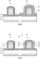
- the figure 1 illustrates a structure from which the steps of the method according to the invention are implemented.
- This structure includes transistors being formed.
- the insulating gate oxide layer 201, 301 is placed in contact with the active layer 103 forming the conduction channel and in contact with the high permittivity layer 202, 302.
- the metal layer 203, 303 is placed in contact with the high permittivity layer 202, 302 and in contact with the gate 204, 304.
- the metallic layer 203, 303 and / or the high permittivity layer 202, 302 are absent.
- the hard mask 205, 305 and a protective layer 400 detailed below are both formed of silicon nitride (SiN).
- a single developed substrate 100 supports a plurality of transistors and therefore gate stacks. For certain applications, it is necessary to have transistors whose properties are different. Thus, some transistors must have a gate oxide 301 whose thickness is greater than that of the gate oxide 201 of other transistors.
- the figure 1 thus represents a grid stack 300, the thickness of the gate oxide 301 of which is greater than that of the oxide of the gate 201 of the stack 200.
- These protective layers 400, 500, 600 are three in number in this exemplary embodiment. However, one could have only two or have four or more.
- the total thickness of the layers forming a spacer on the flanks of the stacks 200 of gates should preferably have a lower thickness. at 9 nm.
- the spacers of transistors of two different types are produced during the same steps.
- the spacers of the transistors having thicker gate oxides are also less than 9 nm.
- this thickness often leads to a breakdown at the level of the spacers of the thick gate oxide transistors, thereby deteriorating the reliability and the service life of devices incorporating this type. of transistors.
- the layers 400 and 600 when they are made of a low-k material, ie with a low permittivity, generally comprise at least one of the following species or a combination of these species: silicon (Si), carbon (C), boron (B), nitrogen (N), hydrogen (H). They are for example formed from one of the following materials: SiCO, SiC, SiCN, SiOCN or SiCBN. These layers are porous or not.
- the dielectric constant of these layers is measured, for example, by the conventional method known as the drop of mercury.
- the layers 400, 500, 600 are all obtained by a conformal deposition, that is to say they have a constant thickness over the entire plate and in particular on the sides 210, 310 and the tops 220, 320 of the stacks. 200, 300 grid as well as outside the 200, 300 grid stacks.
- the figure 2 illustrates a following step during which a masking layer 700 is formed in order to completely cover the second stack 300 of the gate, that is to say that having a thickness of gate oxide 301 greater than that of the first stack 200.
- This masking layer 700 is typically a resin layer, deposited full plate, then opened at the level of the first stack 200 by one of the conventional lithography techniques.
- an organic or organo-mineral material which can be shaped by exposure to a beam of electrons, photons or X-rays or mechanically, is referred to as a resin.
- the next step aims to remove the second protective layer 600 which covers the first stack 200 of the grid. As shown in figure 3 , this step is preferably carried out so as to completely remove the portion of the second protective layer 600 which is located on the first grid pattern 200.
- this layer 600 is etched without etching the first protective layer 500. Furthermore, the second protective layer 600, protected by the masking layer 700, remains in place.
- first protective layer 500 is made of SiO2 and the second protective layer 600 is made of silicon nitride
- this last layer will be selectively removed from the first protective layer 500 by wet etching, for example with a solution based on of H3PO4.
- the second protective layer 600 can also and preferably be removed by dry etching carried out for example in an inductively coupled (ICP), capacitive (CCP) or microwave reactor.
- ICP inductively coupled
- CCP capacitive
- microwave reactor a material with a dielectric constant of less than 7
- fluorine-based chemistry such as a fluorinated or fluorocarbon-based chemistry will be used.
- This type of etching makes it possible to be very selective with respect to SiO2, which is a good candidate for the first protective layer 500.
- the parameters will be adjusted in order to obtain isotropic etching.
- the bias voltage will be lowered in the case of an inductive or capacitive coupled plasma.
- the bias voltage and / or the source voltage can also be pulsed to improve the isotropy of the etching.
- the fluorinated chemistry can be based on CxFyHz, SF6 or NF3 diluted or not with other gases such as HBr, N2, Ar, He, H2, CxHyHz.
- gases such as HBr, N2, Ar, He, H2, CxHyHz.
- the masking layer 700 is then removed. Naturally, this removal is selective for the material of the first layer 500 in order to keep the latter on the first stack 200.
- this masking layer 700 is a photosensitive resin, it is for example removed in a capacitive coupling or coupling reactor. inductive or microwave using oxidative or reducing chemistry.
- a gas mixture of N2 and H2 can be injected into a plasma reactor for etching, then wet cleaning to remove resin residues. This cleaning can be carried out using an SC1 solution.
- the initial thickness of the first layer 500 is retained in its entirety or is at most very little consumed.
- the figures 5 to 7 aim to anisotropically etch the second layer 600 in order to eliminate or reduce the thickness of this layer 600 on the top 320 of the second stack 300 while maintaining a high thickness of this layer 600 on its sides 310 and without significantly altering the first protective layer 500.
- the figure 6 illustrates an anisotropic etching step carried out in a privileged direction 10 which is perpendicular to the main plane in which the substrate 100 extends.
- the protective film 900 if present, is removed on surfaces parallel to the principal plane in which the substrate 100.
- This protective film 900 is removed on the tops 220, 320 of the stacks 200, 300 and between the stacks 200, 300.
- This anisotropic etching also removes part of the thickness of the second protective layer 600 located on the top 320 of the second stack 300.
- This etching etches the second protective layer 600 much faster than the first protective layer 500, so that at the end of this anisotropic etching, the thickness of the first protective layer 500 is not consumed at all. or is only partially engraved on the top 220 of the first stack 200.
- anisotropic etching removes all of the protective film 900 on the top 220, 320 of the stacks 200, 300 and between the latter and consumes about 3 nm of the second protective layer 600 on the top 320 of the second stack 300. It remains then a thickness of 1 nm of the second layer 600 on the top 320.
- the figure 7 illustrates an overetching step to remove the thickness of the second protective layer 600 which remains on the top 320 of the second stack 300.
- This residual thickness is approximately 1 nm in this non-limiting example.
- This etching is selective of the material of this layer 600 with respect to that of the first layer 500 which is not or only little consumed.
- the second layer 600 is then removed everywhere except the sides 310 of the second stack 300.
- the residual portions 610 of the second protective layer 600 then form spacers 610. This etching is preferably anisotropic.
- the method passes directly from the step illustrated in figure 4 at the step illustrated in figure 7 .
- an anisotropic etching is carried out directly from the step illustrated in figure 4 in order to obtain the structure shown in figure 7 .
- the etching carried out so as to remove the second protective layer 600 on the top of the second pattern 300 may possibly result in consuming part of the thickness of the first protective layer 500 located on the first stack 200 of the grid. and especially on the top of the latter.
- this partial consumption is not detrimental because, as will be explained later, the etching of the first protective layer 500 is very selective with respect to the material of the third protective layer 400.
- the first protective layer 500 is a SixOy silicon oxide and the third protective layer 400 is made of SixNy silicon nitride. Consequently, during the removal of the first protective layer 500 on the first and second grid patterns 200, 300 the etching will stop simultaneously on these two patterns 200,300 and without consuming the third protective layer 400 on the first pattern 200.
- the figure 8 illustrates the removal of the first protective layer 500. This removal reveals the third protective layer 400, intended to form the spacers for the first stack 200, that is to say the stack having a low oxide thickness grid 201.
- the second protective layer 500 is entirely removed at least on the first stack or pattern 200. Consequently, the sides 210 of the first pattern 200 are covered by the third protective layer 400 and preferably only by this third. protective layer 400. This makes it possible to preserve the thickness of the standard spacer formed by the third protective layer 400. This makes it possible in particular not to have to modify the standard method concerning the particularly critical steps of defining the thickness of the spacers on grid stacks whose sides are covered by a single-layer spacer.
- the first protective layer 500 is an oxide such as SiO2
- this removal is advantageously carried out by wet etching, for example with a dilute solution of HF.
- This etching etches the first layer 500 selectively to the spacers 610 of the second layer 600 and to the third layer 400, so that the latter is only slightly and preferably is not etched at all.
- This encapsulation layer 1000 is for example a nitride layer (SiN for example) or a low-k layer, that is to say whose dielectric constant is less than 7.
- the thickness of the third protective layer 400 must be chosen to obtain, after deposition of the encapsulation layer 1000, the desired thickness to protect the sides 210 of the first stack 200.
- the structure obtained has the advantage that the active layer 103 is, apart from the grid stacks 200, 300, surmounted by a layer 400 of constant thickness on the plate. Consequently, the same anisotropic etching of the third protective layer 400 makes it possible to remove the latter from either side of the stacks 200, 300 in order to expose the active layer 103 with a view to forming the source and drain, typically by epitaxy from the active layer 103.
- This third layer 400 has a constant thickness makes it possible to control its etching in order to remove it entirely but without altering the underlying active layer 103.
- the etching speed of the third protective layer 400 made of silicon nitride is of the order of 30 nm / min.
- the thicknesses of the first protective layer 500, the second protective layer 600 and the third protective layer 400 only remain on the sides 310 of the second stack 300. Furthermore, on the sides 210 of the first stack 200 only the third layer 400 remains.
- the steps described with reference to figures 9 and 10 are replaced by a step of anisotropic etching of the third protective layer 400 in the preferred direction 10. Consequently, according to this embodiment, the step illustrated in figure 13 follows the step illustrated in figure 8 This print is a dry print. The result of this engraving is illustrated in figure 13 .
- the third protective layer 400 is removed on the tops and between the stacks 200, 300. On the other hand, it remains on the sides 210 of the first stack 200 (as well as on the sides 310 of the second stack 300 since the latter are covered by the others. spacers formed by the first 500 and second 600 layers).
- the steps mentioned below can be performed from the result of the step illustrated in figure 13 .
- This embodiment has the particular advantage of reducing the number of steps and thus being less expensive.
- the third protective layer 400 is intended to form a spacer which will be kept on the flanks of the first gate stack 200 during operation of the transistor.
- the third protective layer 400 thus forms a functional spacers.
- the spacers formed by the first 500; second 600 and third 400 layers are retained. Thus, these layers form functional spacers. They will preferably be present on this second gate stack 300 in the final transistor.
- the total spacer thickness for thick gate oxide transistors is about three times greater than for thin gate oxide transistors. This avoids the risk of breakdown.
- doping is carried out by inclined implantation (tilted doping) of the flanks of the stack 300 having a thicker gate oxide in order to spike the region of the layer 103 located under the spacer.
- This doping makes it possible to maintain or improve the performance of this transistor.
- This doping comprises for example the implantation of Arsenic (As), Phosphorus (P) species for an N type transistor, or Boron (B), boron difluoride (BF2), or Indium for a P type transistor in the region of the channel located under the thicker spacer
- the spacers are formed on either side of the stacks 200, 300. Conventional steps can then be implemented to finalize the production of the transistors.
- the method according to the invention makes it possible to improve the service life of devices integrating transistors whose gate thicknesses are different on the same chip, without increasing significantly. the complexity of the manufacturing process.
- the anisotropic etching step of the second protective layer 600 can be carried out before masking the second stack 300.
- the second protective layer 600 is removed, entirely or partially, on the vertices 220, 320 of the two. stacks 200, 300.
- this layer is preserved on the sides 210, 310 of the two stacks 200, 300.
- the step of masking the second stack 300 is carried out in order to allow isotropic etching of the second layer 600 covering the first stack 200, in particular at its sides 210.
- this alternative embodiment has the following advantages: Although the invention is particularly advantageous for producing on the same substrate transistors whose gate stacks have insulating layers (typically a gate oxide layer) of different thicknesses, this is not limiting. In fact, the invention also applies to the production on the same substrate of transistors whose gate stacks have insulating layers of identical thicknesses.
- insulating layers typically a gate oxide layer
- the grid stack is produced prior to the steps of the invention.
- the functional grid stack is produced after the steps of the invention.
- the grid stack on which the first protective layer is deposited therefore forms a sacrificial pattern which will be removed, once the spacers have been made.
- This alternative embodiment is thus a gate last type process.
Landscapes
- Thin Film Transistor (AREA)
- Formation Of Insulating Films (AREA)
- Internal Circuitry In Semiconductor Integrated Circuit Devices (AREA)
- Insulated Gate Type Field-Effect Transistor (AREA)
- Metal-Oxide And Bipolar Metal-Oxide Semiconductor Integrated Circuits (AREA)
Claims (14)
- Verfahren zur Herstellung auf demselben Substrat (100) vom Typ Silicon-on-Insulator (SOI) oder Fully-Depleted-Silicon-on-Insulator (FDSOI) mindestens eines ersten Transistors und mindestens eines zweiten Transistors, wobei das Verfahren mindestens die folgenden Schritte umfasst:- Herstellen, auf einem Substrat (100), mindestens eines ersten Gittermotivs (200) und mindestens eines zweiten Gittermotivs (300);- Ablagern, auf dem ersten und dem zweiten Gittermotiv (200, 300), mindestens:die zweite Schutzschicht (600) und die dritte Schutzschicht (400) jeweils aus einem Material von den folgenden Materialien gemacht sind: Siliciumnitrid (SiN), Materialien, deren dielektrische Konstante k kleiner als 7 ist, SiCO, SiC, SiCN, SiOCN, SiCBN;• einer ersten Schutzschicht (500),• einer zweiten Schutzschicht (600), die die erste Schutzschicht (500) überlagert und aus einem Material gemacht ist, das sich von dem der ersten Schutzschicht (500) unterscheidet,• einer dritten Schutzschicht (400), die von der ersten Schutzschicht (500) und von der zweiten Schutzschicht (600) überlagert ist, wobei die dritte Schutzschicht (400) aus einem Material ist, das eine Gravur des Materials der ersten Schutzschicht (500) selektiv zum Material der dritten Schutzschicht (400) erlaubt, und- Maskieren des zweiten Gittermotivs durch eine Maskierungsschicht (700);- isotropes Gravieren der zweiten Schutzschicht (600), die sich auf dem ersten Gittermotiv (200) befindet, derart, dass die zweite Schutzschicht (600), die sich auf dem ersten Gittermotiv (200) befindet, vollständig entfernt wird, bei Beibehaltung der ersten Schutzschicht (500) auf dem ersten Gittermotiv (200), wobei bei dieser isotropen Gravur das zweite Gittermotiv (300) von der Maskierungsschicht (700) maskiert wird;- Entfernen der Maskierungsschicht (700) nach dem Schritt der isotropen Gravur;- vor dem Maskierungsschritt oder nach dem Schritt des Entfernens der Maskierungsschicht (700): anisotrope Gravur der zweiten Schutzschicht (600) selektiv zu der ersten Schutzschicht (500) derart, dass die zweite Schutzschicht (600) mindestens teilweise entfernt wird, die sich auf einer Spitze (320) des zweiten Gittermotivs (300) befindet, und mindestens ein Teil der Dicke der zweiten Schutzschicht (600) beibehalten wird, die sich auf den Flanken (310) des zweiten Gittermotivs (300) befindet,- vor dem Schritt des Ablagerns der ersten und der zweiten Schutzschicht (500, 600), einen Schritt des Ablagerns auf dem ersten und zweiten Gittermotiv (200, 300) der dritten Schutzschicht (400), die unter der ersten Schutzschicht (500) angeordnet ist und das erste und zweite Gittermotiv (200, 300) bedeckt,- nach der anisotropen Gravur der zweiten Schutzschicht (600) selektiv zu der ersten Schutzschicht (500): einen Gravurschritt der ersten Schutzschicht (500) selektiv zu der dritten Schutzschicht (400), so dass die erste Schutzschicht (500) auf dem ersten Gittermotiv (200) vorzugweise vollständig entfernt und die dritte Schutzschicht (400) beibehalten wird.
- Verfahren nach vorangehendem Anspruch, wobei das erste Gittermotiv (200) ein erster Gitterstapel ist und wobei das zweite Gittermotiv (300) ein zweiter Gitterstapel ist, wobei jeder von dem ersten und zweiten Gitterstapel mindestens eine Isolierschicht (201, 301), in typischer Weise ein Gitteroxid, umfasst.
- Verfahren nach Anspruch 1, wobei das erste Gittermotiv (200) ein Opfermotiv ist, wobei das zweite Motiv (300) ein Opfermotiv ist, wobei das Verfahren nach dem anisotropen Gravurschritt der zweiten Schutzschicht (600) selektiv zu der ersten Schutzschicht (500) einen Schritt des Ersetzens des ersten und zweiten Opfermotivs (200, 300) durch Motive ist, die jeweils einen ersten Gitterstapel und einen zweiten Gitterstapel bilden, wobei jeder von dem ersten und zweiten Gitterstapel mindestens eine Isolierschicht (201, 301), in typischer Weise ein Gitteroxid, umfasst.
- Verfahren nach einem der zwei vorangehenden Ansprüche, wobei die Dicke der Isolierschicht (301) des zweiten Stapels größer als die Dicke der Isolierschicht (201) des ersten Stapels ist.
- Verfahren nach einem der vorangehenden Ansprüche, wobei die zweite Schutzschicht (600) und die dritte Schutzschicht (400) porös sind oder nicht.
- Verfahren nach einem der vorangehenden Ansprüche, wobei die dritte Schutzschicht (400) eine Dicke aufweist, die zwischen 3 und 10 nm (10-9 Meter) und vorzugsweise zwischen 4 und 8 nm (10-9 Meter) liegt.
- Verfahren nach einem der vorangehenden Ansprüche, wobei die Ablagerung von mindestens einer von der ersten (500), der zweiten (600) und der dritten (400) Schutzschicht eine konforme Ablagerung ist und wobei vorzugsweise jede der Ablagerungen der ersten (500), zweiten (600) und dritten (400) Schutzschicht eine konforme Ablagerung ist.
- Verfahren nach einem der vorangehenden Ansprüche, umfassend, nach dem anisotropen Gravurschritt der zweiten Schutzschicht (600), einen Schritt des Entfernens der ersten Schutzschicht (500), die sich auf der Spitze (320) des zweiten Gittermotivs (300), auf dem ersten Gittermotiv (200) und zwischen dem ersten und zweiten Gittermotiv (200, 300) befindet, durch selektive Gravur des Materials der ersten Schutzschicht (500) gegenüber dem Material der zweiten Schutzschicht (600) und dem Material der dritten Schutzschicht (400).
- Verfahren nach vorangehendem Anspruch, umfassend, nach dem Schritt des Entfernens der ersten Schicht (500) auf dem ersten Gittermotiv (200), einen Schritt des Ablagerns einer Kapselschicht (1000) aus einem Material, das eine dielektrische Konstante kleiner oder gleich 8 aufweist, auf mindestens dem zweiten Gittermotiv (300).
- Verfahren nach einem der vorangehenden Ansprüche, wobei die erste Schutzschicht (500) ein Oxid ist, vorzugsweise Siliciumoxid (SiO2).
- Verfahren nach einem der vorangehenden Ansprüche, wobei der isotrope Gravurschritt der zweiten Schutzschicht (600) eine feuchte Gravur ist, vorzugsweise auf der Basis einer H3PO4-Lösung.
- Verfahren nach einem der Ansprüche 1 bis 10, wobei der isotrope Gravurschritt der zweiten Schutzschicht (600) eine trockene Gravur ist, die vorzugsweise Fluorcarbon- oder Fluorchemie verwendet, und wobei die trockene Gravur vorzugsweise in einem Plasmareaktor durchgeführt wird, in dem eine Polarisationsspannung oder die Quellspannung gepulst wird.
- Verfahren nach einem der vorangehenden Ansprüche, wobei die zweite Schutzschicht (600) ein Nitrid oder ein Material ist, das eine dielektrische Konstante unter 7 aufweist und der anisotrope Gravurschritt der zweiten Schutzschicht (600) umfasst:- einen Schritt des Schützens durch Bilden eines Oxidschutzfilms (900) auf dem ersten und zweiten Gittermotiv (200, 300);- das anisotrope Gravieren des Oxidschutzfilms (900) außerhalb der Flanken (210, 310) des ersten und zweiten Gittermotivs (200, 300) derart, dass der Oxidschutzfilm (900) nur auf den Flanken (210, 310) des ersten und zweiten Gittermotivs (200, 300) beibehalten wird;- das Gravieren mindestens eines Teils der zweiten Schutzschicht (600), die sich auf einer Spitze (320) und beiderseits des zweiten Gittermotivs (300) befindet, wobei die Gravur selektiv gegenüber dem Oxidschutzfilm (900) ist, der sich auf den Flanken (210, 310) des ersten und zweiten Gittermotivs (200, 300) und der ersten Schutzschicht (500) befindet, die sich auf der Spitze (220) des ersten Gittermotivs (200) befindet.
- Verfahren nach einem der vorangehenden Ansprüche, wobei die zweite Schutzschicht (600) aus Nitrid, vorzugsweise aus Siliciumnitrid (SiN) oder aus einem Material ist, dessen dielektrische Konstante kleiner als 7 ist, die erste Schutzschicht (500) ein Oxid ist, vorzugsweise ein Siliciumoxid (SiO2), und der Schutzfilm (900) aus einem Plasma auf der Basis von Sauerstoff gebildet ist.
Applications Claiming Priority (1)
| Application Number | Priority Date | Filing Date | Title |
|---|---|---|---|
| FR1654554A FR3051597B1 (fr) | 2016-05-20 | 2016-05-20 | Procede de realisation sur un meme substrat de transistors presentant des caracteristiques differentes |
Publications (2)
| Publication Number | Publication Date |
|---|---|
| EP3246948A1 EP3246948A1 (de) | 2017-11-22 |
| EP3246948B1 true EP3246948B1 (de) | 2020-11-18 |
Family
ID=56148592
Family Applications (1)
| Application Number | Title | Priority Date | Filing Date |
|---|---|---|---|
| EP17171978.4A Active EP3246948B1 (de) | 2016-05-20 | 2017-05-19 | Verfahren zur herstellung von transistoren, die unterschiedliche eigenschaften aufweisen, auf demselben substrat |
Country Status (3)
| Country | Link |
|---|---|
| US (1) | US10347545B2 (de) |
| EP (1) | EP3246948B1 (de) |
| FR (1) | FR3051597B1 (de) |
Families Citing this family (4)
| Publication number | Priority date | Publication date | Assignee | Title |
|---|---|---|---|---|
| KR102458310B1 (ko) * | 2018-06-19 | 2022-10-24 | 삼성전자주식회사 | 집적회로 소자 |
| FR3090997A1 (fr) * | 2018-12-20 | 2020-06-26 | Commissariat A L'energie Atomique Et Aux Energies Alternatives | Procédé de réalisation d’un transistor à source et drain surélevés |
| FR3091002B1 (fr) | 2018-12-20 | 2021-01-08 | Commissariat Energie Atomique | Procédé de gravure d’une couche diélectrique tridimensionnelle |
| FR3113770B1 (fr) | 2020-08-31 | 2025-09-26 | Commissariat Energie Atomique | Procédé de fabrication de composants micro-électroniques |
Family Cites Families (7)
| Publication number | Priority date | Publication date | Assignee | Title |
|---|---|---|---|---|
| JP4746332B2 (ja) * | 2005-03-10 | 2011-08-10 | Okiセミコンダクタ株式会社 | 半導体装置の製造方法 |
| CN102299154B (zh) * | 2010-06-22 | 2013-06-12 | 中国科学院微电子研究所 | 半导体结构及其制作方法 |
| JP2012084636A (ja) * | 2010-10-08 | 2012-04-26 | Panasonic Corp | 半導体装置及びその製造方法 |
| US8450169B2 (en) * | 2010-11-29 | 2013-05-28 | International Business Machines Corporation | Replacement metal gate structures providing independent control on work function and gate leakage current |
| WO2014162164A1 (en) * | 2013-04-03 | 2014-10-09 | Commissariat A L'energie Atomique Et Aux Eneriges Alternatives | Cmos in situ doped flow with independently tunable spacer thickness |
| US20160003584A1 (en) * | 2013-07-09 | 2016-01-07 | Eric Durynski | Portable bullet trap |
| US9252147B2 (en) | 2013-08-05 | 2016-02-02 | Qualcomm Incorporated | Methods and apparatuses for forming multiple radio frequency (RF) components associated with different RF bands on a chip |
-
2016
- 2016-05-20 FR FR1654554A patent/FR3051597B1/fr not_active Expired - Fee Related
-
2017
- 2017-05-19 EP EP17171978.4A patent/EP3246948B1/de active Active
- 2017-05-19 US US15/599,944 patent/US10347545B2/en active Active
Non-Patent Citations (1)
| Title |
|---|
| None * |
Also Published As
| Publication number | Publication date |
|---|---|
| US20170358502A1 (en) | 2017-12-14 |
| EP3246948A1 (de) | 2017-11-22 |
| FR3051597B1 (fr) | 2019-11-08 |
| US10347545B2 (en) | 2019-07-09 |
| FR3051597A1 (fr) | 2017-11-24 |
Similar Documents
| Publication | Publication Date | Title |
|---|---|---|
| EP2876677B1 (de) | Verfahren zur Bildung von Abstandhaltern eines Gates eines Transistors | |
| EP3246953B1 (de) | Verfahren zur herstellung von transistoren, die unterschiedliche eigenschaften aufweisen, auf demselben substrat | |
| EP2999001B1 (de) | Einbringung von abstandhaltern an den seiten eines transistor-gates | |
| EP3261124B1 (de) | Verfahren zur bildung von abstandhaltern eines gates eines transistors | |
| EP2779223B1 (de) | Herstellungsverfahren eines Substrats, das mit einem Kantenschutz ausgestattet ist | |
| EP3246948B1 (de) | Verfahren zur herstellung von transistoren, die unterschiedliche eigenschaften aufweisen, auf demselben substrat | |
| EP3249689B1 (de) | Verfahren zur bildung von pdsoi- und fdsoi-transistoren auf demselben substrat | |
| EP3396704B1 (de) | Gravierverfahren einer schicht auf sin-basis | |
| EP2610915A1 (de) | Transistor und Herstellungsverfahren eines Transistors | |
| EP3506336B1 (de) | Ätzverfahren einer dielektrischen 3d-schicht | |
| FR3080486A1 (fr) | Procede de formation d'un dispositif microelectronique | |
| FR3047352A1 (fr) | Procede de fabrication d'un transistor a dopant localise a l'aplomb de la grille | |
| WO2014037411A1 (fr) | Procédé de réalisation de transistors fet | |
| EP3671815B1 (de) | Gravurverfahren einer dielektrischen 3d-schicht | |
| EP2613342B1 (de) | Verfahren zur Herstellung einer nicht-flüchtigen Speicherzelle mit Doppel-Gate | |
| EP3764390B1 (de) | Verfahren zur bildung von abstandhaltern für einen transistor | |
| FR3125916A1 (fr) | Procede de realisation de portions dielectriques laterales | |
| FR3023408A1 (fr) | Procede de fabrication d'une cellule memoire a double grille | |
| EP3503203A1 (de) | Herstellung von transistoren mit unter spannung stehenden kanälen | |
| WO2025140898A1 (fr) | Procédé de réalisation d'un dispositif microélectronique sur substrat fd-soi, dispositif correspondant et circuit intégré l'incorporant | |
| FR3076397A1 (fr) | Procede de fabrication d'un transistor | |
| EP4002482A1 (de) | Verfahren zur herstellung eines bereichs, der mit einer mikroelektronischen vorrichtung dotiert ist | |
| FR3098978A1 (fr) | procédé de fabrication de transistors |
Legal Events
| Date | Code | Title | Description |
|---|---|---|---|
| PUAI | Public reference made under article 153(3) epc to a published international application that has entered the european phase |
Free format text: ORIGINAL CODE: 0009012 |
|
| STAA | Information on the status of an ep patent application or granted ep patent |
Free format text: STATUS: REQUEST FOR EXAMINATION WAS MADE |
|
| 17P | Request for examination filed |
Effective date: 20170519 |
|
| AK | Designated contracting states |
Kind code of ref document: A1 Designated state(s): AL AT BE BG CH CY CZ DE DK EE ES FI FR GB GR HR HU IE IS IT LI LT LU LV MC MK MT NL NO PL PT RO RS SE SI SK SM TR |
|
| AX | Request for extension of the european patent |
Extension state: BA ME |
|
| RIC1 | Information provided on ipc code assigned before grant |
Ipc: H01L 27/12 20060101AFI20200313BHEP Ipc: H01L 29/66 20060101ALI20200313BHEP Ipc: H01L 21/84 20060101ALI20200313BHEP |
|
| GRAP | Despatch of communication of intention to grant a patent |
Free format text: ORIGINAL CODE: EPIDOSNIGR1 |
|
| STAA | Information on the status of an ep patent application or granted ep patent |
Free format text: STATUS: GRANT OF PATENT IS INTENDED |
|
| INTG | Intention to grant announced |
Effective date: 20200612 |
|
| RAP1 | Party data changed (applicant data changed or rights of an application transferred) |
Owner name: COMMISSARIAT A L'ENERGIE ATOMIQUE ET AUX ENERGIES ALTERNATIVES |
|
| GRAS | Grant fee paid |
Free format text: ORIGINAL CODE: EPIDOSNIGR3 |
|
| GRAA | (expected) grant |
Free format text: ORIGINAL CODE: 0009210 |
|
| STAA | Information on the status of an ep patent application or granted ep patent |
Free format text: STATUS: THE PATENT HAS BEEN GRANTED |
|
| AK | Designated contracting states |
Kind code of ref document: B1 Designated state(s): AL AT BE BG CH CY CZ DE DK EE ES FI FR GB GR HR HU IE IS IT LI LT LU LV MC MK MT NL NO PL PT RO RS SE SI SK SM TR |
|
| REG | Reference to a national code |
Ref country code: GB Ref legal event code: FG4D Free format text: NOT ENGLISH |
|
| REG | Reference to a national code |
Ref country code: CH Ref legal event code: EP |
|
| REG | Reference to a national code |
Ref country code: IE Ref legal event code: FG4D Free format text: LANGUAGE OF EP DOCUMENT: FRENCH |
|
| REG | Reference to a national code |
Ref country code: DE Ref legal event code: R096 Ref document number: 602017027621 Country of ref document: DE |
|
| REG | Reference to a national code |
Ref country code: AT Ref legal event code: REF Ref document number: 1336713 Country of ref document: AT Kind code of ref document: T Effective date: 20201215 |
|
| REG | Reference to a national code |
Ref country code: AT Ref legal event code: MK05 Ref document number: 1336713 Country of ref document: AT Kind code of ref document: T Effective date: 20201118 |
|
| REG | Reference to a national code |
Ref country code: NL Ref legal event code: MP Effective date: 20201118 |
|
| PG25 | Lapsed in a contracting state [announced via postgrant information from national office to epo] |
Ref country code: NO Free format text: LAPSE BECAUSE OF FAILURE TO SUBMIT A TRANSLATION OF THE DESCRIPTION OR TO PAY THE FEE WITHIN THE PRESCRIBED TIME-LIMIT Effective date: 20210218 Ref country code: PT Free format text: LAPSE BECAUSE OF FAILURE TO SUBMIT A TRANSLATION OF THE DESCRIPTION OR TO PAY THE FEE WITHIN THE PRESCRIBED TIME-LIMIT Effective date: 20210318 Ref country code: RS Free format text: LAPSE BECAUSE OF FAILURE TO SUBMIT A TRANSLATION OF THE DESCRIPTION OR TO PAY THE FEE WITHIN THE PRESCRIBED TIME-LIMIT Effective date: 20201118 Ref country code: FI Free format text: LAPSE BECAUSE OF FAILURE TO SUBMIT A TRANSLATION OF THE DESCRIPTION OR TO PAY THE FEE WITHIN THE PRESCRIBED TIME-LIMIT Effective date: 20201118 Ref country code: GR Free format text: LAPSE BECAUSE OF FAILURE TO SUBMIT A TRANSLATION OF THE DESCRIPTION OR TO PAY THE FEE WITHIN THE PRESCRIBED TIME-LIMIT Effective date: 20210219 |
|
| PG25 | Lapsed in a contracting state [announced via postgrant information from national office to epo] |
Ref country code: SE Free format text: LAPSE BECAUSE OF FAILURE TO SUBMIT A TRANSLATION OF THE DESCRIPTION OR TO PAY THE FEE WITHIN THE PRESCRIBED TIME-LIMIT Effective date: 20201118 Ref country code: BG Free format text: LAPSE BECAUSE OF FAILURE TO SUBMIT A TRANSLATION OF THE DESCRIPTION OR TO PAY THE FEE WITHIN THE PRESCRIBED TIME-LIMIT Effective date: 20210218 Ref country code: IS Free format text: LAPSE BECAUSE OF FAILURE TO SUBMIT A TRANSLATION OF THE DESCRIPTION OR TO PAY THE FEE WITHIN THE PRESCRIBED TIME-LIMIT Effective date: 20210318 Ref country code: LV Free format text: LAPSE BECAUSE OF FAILURE TO SUBMIT A TRANSLATION OF THE DESCRIPTION OR TO PAY THE FEE WITHIN THE PRESCRIBED TIME-LIMIT Effective date: 20201118 Ref country code: PL Free format text: LAPSE BECAUSE OF FAILURE TO SUBMIT A TRANSLATION OF THE DESCRIPTION OR TO PAY THE FEE WITHIN THE PRESCRIBED TIME-LIMIT Effective date: 20201118 Ref country code: AT Free format text: LAPSE BECAUSE OF FAILURE TO SUBMIT A TRANSLATION OF THE DESCRIPTION OR TO PAY THE FEE WITHIN THE PRESCRIBED TIME-LIMIT Effective date: 20201118 |
|
| REG | Reference to a national code |
Ref country code: LT Ref legal event code: MG9D |
|
| PG25 | Lapsed in a contracting state [announced via postgrant information from national office to epo] |
Ref country code: HR Free format text: LAPSE BECAUSE OF FAILURE TO SUBMIT A TRANSLATION OF THE DESCRIPTION OR TO PAY THE FEE WITHIN THE PRESCRIBED TIME-LIMIT Effective date: 20201118 |
|
| PG25 | Lapsed in a contracting state [announced via postgrant information from national office to epo] |
Ref country code: RO Free format text: LAPSE BECAUSE OF FAILURE TO SUBMIT A TRANSLATION OF THE DESCRIPTION OR TO PAY THE FEE WITHIN THE PRESCRIBED TIME-LIMIT Effective date: 20201118 Ref country code: SK Free format text: LAPSE BECAUSE OF FAILURE TO SUBMIT A TRANSLATION OF THE DESCRIPTION OR TO PAY THE FEE WITHIN THE PRESCRIBED TIME-LIMIT Effective date: 20201118 Ref country code: EE Free format text: LAPSE BECAUSE OF FAILURE TO SUBMIT A TRANSLATION OF THE DESCRIPTION OR TO PAY THE FEE WITHIN THE PRESCRIBED TIME-LIMIT Effective date: 20201118 Ref country code: CZ Free format text: LAPSE BECAUSE OF FAILURE TO SUBMIT A TRANSLATION OF THE DESCRIPTION OR TO PAY THE FEE WITHIN THE PRESCRIBED TIME-LIMIT Effective date: 20201118 Ref country code: SM Free format text: LAPSE BECAUSE OF FAILURE TO SUBMIT A TRANSLATION OF THE DESCRIPTION OR TO PAY THE FEE WITHIN THE PRESCRIBED TIME-LIMIT Effective date: 20201118 Ref country code: LT Free format text: LAPSE BECAUSE OF FAILURE TO SUBMIT A TRANSLATION OF THE DESCRIPTION OR TO PAY THE FEE WITHIN THE PRESCRIBED TIME-LIMIT Effective date: 20201118 |
|
| REG | Reference to a national code |
Ref country code: DE Ref legal event code: R097 Ref document number: 602017027621 Country of ref document: DE |
|
| PG25 | Lapsed in a contracting state [announced via postgrant information from national office to epo] |
Ref country code: DK Free format text: LAPSE BECAUSE OF FAILURE TO SUBMIT A TRANSLATION OF THE DESCRIPTION OR TO PAY THE FEE WITHIN THE PRESCRIBED TIME-LIMIT Effective date: 20201118 |
|
| PGFP | Annual fee paid to national office [announced via postgrant information from national office to epo] |
Ref country code: GB Payment date: 20210514 Year of fee payment: 5 |
|
| PLBE | No opposition filed within time limit |
Free format text: ORIGINAL CODE: 0009261 |
|
| STAA | Information on the status of an ep patent application or granted ep patent |
Free format text: STATUS: NO OPPOSITION FILED WITHIN TIME LIMIT |
|
| 26N | No opposition filed |
Effective date: 20210819 |
|
| PG25 | Lapsed in a contracting state [announced via postgrant information from national office to epo] |
Ref country code: NL Free format text: LAPSE BECAUSE OF FAILURE TO SUBMIT A TRANSLATION OF THE DESCRIPTION OR TO PAY THE FEE WITHIN THE PRESCRIBED TIME-LIMIT Effective date: 20201118 Ref country code: AL Free format text: LAPSE BECAUSE OF FAILURE TO SUBMIT A TRANSLATION OF THE DESCRIPTION OR TO PAY THE FEE WITHIN THE PRESCRIBED TIME-LIMIT Effective date: 20201118 |
|
| PG25 | Lapsed in a contracting state [announced via postgrant information from national office to epo] |
Ref country code: SI Free format text: LAPSE BECAUSE OF FAILURE TO SUBMIT A TRANSLATION OF THE DESCRIPTION OR TO PAY THE FEE WITHIN THE PRESCRIBED TIME-LIMIT Effective date: 20201118 |
|
| REG | Reference to a national code |
Ref country code: CH Ref legal event code: PL |
|
| PG25 | Lapsed in a contracting state [announced via postgrant information from national office to epo] |
Ref country code: CH Free format text: LAPSE BECAUSE OF NON-PAYMENT OF DUE FEES Effective date: 20210531 Ref country code: LI Free format text: LAPSE BECAUSE OF NON-PAYMENT OF DUE FEES Effective date: 20210531 Ref country code: MC Free format text: LAPSE BECAUSE OF FAILURE TO SUBMIT A TRANSLATION OF THE DESCRIPTION OR TO PAY THE FEE WITHIN THE PRESCRIBED TIME-LIMIT Effective date: 20201118 Ref country code: LU Free format text: LAPSE BECAUSE OF NON-PAYMENT OF DUE FEES Effective date: 20210519 Ref country code: ES Free format text: LAPSE BECAUSE OF FAILURE TO SUBMIT A TRANSLATION OF THE DESCRIPTION OR TO PAY THE FEE WITHIN THE PRESCRIBED TIME-LIMIT Effective date: 20201118 |
|
| REG | Reference to a national code |
Ref country code: BE Ref legal event code: MM Effective date: 20210531 |
|
| PG25 | Lapsed in a contracting state [announced via postgrant information from national office to epo] |
Ref country code: IE Free format text: LAPSE BECAUSE OF NON-PAYMENT OF DUE FEES Effective date: 20210519 |
|
| PG25 | Lapsed in a contracting state [announced via postgrant information from national office to epo] |
Ref country code: IS Free format text: LAPSE BECAUSE OF FAILURE TO SUBMIT A TRANSLATION OF THE DESCRIPTION OR TO PAY THE FEE WITHIN THE PRESCRIBED TIME-LIMIT Effective date: 20210318 |
|
| PG25 | Lapsed in a contracting state [announced via postgrant information from national office to epo] |
Ref country code: BE Free format text: LAPSE BECAUSE OF NON-PAYMENT OF DUE FEES Effective date: 20210531 |
|
| GBPC | Gb: european patent ceased through non-payment of renewal fee |
Effective date: 20220519 |
|
| PG25 | Lapsed in a contracting state [announced via postgrant information from national office to epo] |
Ref country code: HU Free format text: LAPSE BECAUSE OF FAILURE TO SUBMIT A TRANSLATION OF THE DESCRIPTION OR TO PAY THE FEE WITHIN THE PRESCRIBED TIME-LIMIT; INVALID AB INITIO Effective date: 20170519 Ref country code: GB Free format text: LAPSE BECAUSE OF NON-PAYMENT OF DUE FEES Effective date: 20220519 |
|
| PG25 | Lapsed in a contracting state [announced via postgrant information from national office to epo] |
Ref country code: CY Free format text: LAPSE BECAUSE OF FAILURE TO SUBMIT A TRANSLATION OF THE DESCRIPTION OR TO PAY THE FEE WITHIN THE PRESCRIBED TIME-LIMIT Effective date: 20201118 |
|
| PG25 | Lapsed in a contracting state [announced via postgrant information from national office to epo] |
Ref country code: MK Free format text: LAPSE BECAUSE OF FAILURE TO SUBMIT A TRANSLATION OF THE DESCRIPTION OR TO PAY THE FEE WITHIN THE PRESCRIBED TIME-LIMIT Effective date: 20201118 |
|
| PG25 | Lapsed in a contracting state [announced via postgrant information from national office to epo] |
Ref country code: MT Free format text: LAPSE BECAUSE OF FAILURE TO SUBMIT A TRANSLATION OF THE DESCRIPTION OR TO PAY THE FEE WITHIN THE PRESCRIBED TIME-LIMIT Effective date: 20201118 |
|
| REG | Reference to a national code |
Ref country code: DE Ref legal event code: R079 Ref document number: 602017027621 Country of ref document: DE Free format text: PREVIOUS MAIN CLASS: H01L0027120000 Ipc: H10D0086000000 |
|
| PGFP | Annual fee paid to national office [announced via postgrant information from national office to epo] |
Ref country code: DE Payment date: 20250519 Year of fee payment: 9 |
|
| PGFP | Annual fee paid to national office [announced via postgrant information from national office to epo] |
Ref country code: IT Payment date: 20250530 Year of fee payment: 9 |
|
| PGFP | Annual fee paid to national office [announced via postgrant information from national office to epo] |
Ref country code: FR Payment date: 20250526 Year of fee payment: 9 |
|
| PG25 | Lapsed in a contracting state [announced via postgrant information from national office to epo] |
Ref country code: TR Free format text: LAPSE BECAUSE OF FAILURE TO SUBMIT A TRANSLATION OF THE DESCRIPTION OR TO PAY THE FEE WITHIN THE PRESCRIBED TIME-LIMIT Effective date: 20201118 |