EP3247013A1 - Elektronische steuerungsvorrichtung - Google Patents
Elektronische steuerungsvorrichtung Download PDFInfo
- Publication number
- EP3247013A1 EP3247013A1 EP16737292.9A EP16737292A EP3247013A1 EP 3247013 A1 EP3247013 A1 EP 3247013A1 EP 16737292 A EP16737292 A EP 16737292A EP 3247013 A1 EP3247013 A1 EP 3247013A1
- Authority
- EP
- European Patent Office
- Prior art keywords
- opening
- case
- control device
- electronic control
- connector
- Prior art date
- Legal status (The legal status is an assumption and is not a legal conclusion. Google has not performed a legal analysis and makes no representation as to the accuracy of the status listed.)
- Granted
Links
Images




Classifications
-
- B—PERFORMING OPERATIONS; TRANSPORTING
- B60—VEHICLES IN GENERAL
- B60R—VEHICLES, VEHICLE FITTINGS, OR VEHICLE PARTS, NOT OTHERWISE PROVIDED FOR
- B60R16/00—Electric or fluid circuits specially adapted for vehicles and not otherwise provided for; Arrangement of elements of electric or fluid circuits specially adapted for vehicles and not otherwise provided for
- B60R16/02—Electric or fluid circuits specially adapted for vehicles and not otherwise provided for; Arrangement of elements of electric or fluid circuits specially adapted for vehicles and not otherwise provided for electric constitutive elements
- B60R16/023—Electric or fluid circuits specially adapted for vehicles and not otherwise provided for; Arrangement of elements of electric or fluid circuits specially adapted for vehicles and not otherwise provided for electric constitutive elements for transmission of signals between vehicle parts or subsystems
- B60R16/0239—Electronic boxes
-
- H—ELECTRICITY
- H01—ELECTRIC ELEMENTS
- H01R—ELECTRICALLY-CONDUCTIVE CONNECTIONS; STRUCTURAL ASSOCIATIONS OF A PLURALITY OF MUTUALLY-INSULATED ELECTRICAL CONNECTING ELEMENTS; COUPLING DEVICES; CURRENT COLLECTORS
- H01R12/00—Structural associations of a plurality of mutually-insulated electrical connecting elements, specially adapted for printed circuits, e.g. printed circuit boards [PCB], flat or ribbon cables, or like generally planar structures, e.g. terminal strips, terminal blocks; Coupling devices specially adapted for printed circuits, flat or ribbon cables, or like generally planar structures; Terminals specially adapted for contact with, or insertion into, printed circuits, flat or ribbon cables, or like generally planar structures
- H01R12/70—Coupling devices
- H01R12/71—Coupling devices for rigid printing circuits or like structures
- H01R12/712—Coupling devices for rigid printing circuits or like structures co-operating with the surface of the printed circuit or with a coupling device exclusively provided on the surface of the printed circuit
- H01R12/716—Coupling device provided on the PCB
-
- H—ELECTRICITY
- H01—ELECTRIC ELEMENTS
- H01R—ELECTRICALLY-CONDUCTIVE CONNECTIONS; STRUCTURAL ASSOCIATIONS OF A PLURALITY OF MUTUALLY-INSULATED ELECTRICAL CONNECTING ELEMENTS; COUPLING DEVICES; CURRENT COLLECTORS
- H01R13/00—Details of coupling devices of the kinds covered by groups H01R12/70 or H01R24/00 - H01R33/00
- H01R13/46—Bases; Cases
- H01R13/516—Means for holding or embracing insulating body, e.g. casing, hoods
- H01R13/518—Means for holding or embracing insulating body, e.g. casing, hoods for holding or embracing several coupling parts, e.g. frames
-
- H—ELECTRICITY
- H01—ELECTRIC ELEMENTS
- H01R—ELECTRICALLY-CONDUCTIVE CONNECTIONS; STRUCTURAL ASSOCIATIONS OF A PLURALITY OF MUTUALLY-INSULATED ELECTRICAL CONNECTING ELEMENTS; COUPLING DEVICES; CURRENT COLLECTORS
- H01R24/00—Two-part coupling devices, or either of their cooperating parts, characterised by their overall structure
- H01R24/76—Two-part coupling devices, or either of their cooperating parts, characterised by their overall structure with sockets, clips or analogous contacts and secured to apparatus or structure, e.g. to a wall
-
- H—ELECTRICITY
- H02—GENERATION; CONVERSION OR DISTRIBUTION OF ELECTRIC POWER
- H02G—INSTALLATION OF ELECTRIC CABLES OR LINES, OR OF COMBINED OPTICAL AND ELECTRIC CABLES OR LINES
- H02G3/00—Installations of electric cables or lines or protective tubing therefor in or on buildings, equivalent structures or vehicles
- H02G3/02—Details
- H02G3/08—Distribution boxes; Connection or junction boxes
- H02G3/16—Distribution boxes; Connection or junction boxes structurally associated with support for line-connecting terminals within the box
-
- H—ELECTRICITY
- H05—ELECTRIC TECHNIQUES NOT OTHERWISE PROVIDED FOR
- H05K—PRINTED CIRCUITS; CASINGS OR CONSTRUCTIONAL DETAILS OF ELECTRIC APPARATUS; MANUFACTURE OF ASSEMBLAGES OF ELECTRICAL COMPONENTS
- H05K5/00—Casings, cabinets or drawers for electric apparatus
- H05K5/0026—Casings, cabinets or drawers for electric apparatus provided with connectors and printed circuit boards [PCB], e.g. automotive electronic control units
- H05K5/0069—Casings, cabinets or drawers for electric apparatus provided with connectors and printed circuit boards [PCB], e.g. automotive electronic control units having connector relating features for connecting the connector pins with the PCB or for mounting the connector body with the housing
-
- H—ELECTRICITY
- H05—ELECTRIC TECHNIQUES NOT OTHERWISE PROVIDED FOR
- H05K—PRINTED CIRCUITS; CASINGS OR CONSTRUCTIONAL DETAILS OF ELECTRIC APPARATUS; MANUFACTURE OF ASSEMBLAGES OF ELECTRICAL COMPONENTS
- H05K7/00—Constructional details common to different types of electric apparatus
- H05K7/20—Modifications to facilitate cooling, ventilating, or heating
- H05K7/20845—Modifications to facilitate cooling, ventilating, or heating for automotive electronic casings
- H05K7/20854—Heat transfer by conduction from internal heat source to heat radiating structure
-
- H—ELECTRICITY
- H01—ELECTRIC ELEMENTS
- H01R—ELECTRICALLY-CONDUCTIVE CONNECTIONS; STRUCTURAL ASSOCIATIONS OF A PLURALITY OF MUTUALLY-INSULATED ELECTRICAL CONNECTING ELEMENTS; COUPLING DEVICES; CURRENT COLLECTORS
- H01R2107/00—Four or more poles
-
- H—ELECTRICITY
- H05—ELECTRIC TECHNIQUES NOT OTHERWISE PROVIDED FOR
- H05K—PRINTED CIRCUITS; CASINGS OR CONSTRUCTIONAL DETAILS OF ELECTRIC APPARATUS; MANUFACTURE OF ASSEMBLAGES OF ELECTRICAL COMPONENTS
- H05K7/00—Constructional details common to different types of electric apparatus
- H05K7/20—Modifications to facilitate cooling, ventilating, or heating
- H05K7/2039—Modifications to facilitate cooling, ventilating, or heating characterised by the heat transfer by conduction from the heat generating element to a dissipating body
- H05K7/20409—Outer radiating structures on heat dissipating housings, e.g. fins integrated with the housing
Definitions
- the present invention relates to an electronic control device.
- An increase of a size of a case and an increase of the number of connector poles have advanced due to an increase in the level of functionality of electronic control devices, beyond technological progress of miniaturization of electronic components mounted on a board and miniaturization of a mounting structure.
- the number of terminal poles of the connector increases, the number of connectors increases or a size of the connector increases.
- the increase of the size of the connector is a custom-order which is expensive, and it is cheaper to dispose a plurality of general-purpose connectors.
- a copper-based material is predominantly used for a wire harness connected to the connector so that it is difficult to make a wire diameter thin in a current situation
- current capacity is also increased due to the increase in the level of functionality in an electronic control device for a direct injection engine with high fuel consumption, and it is difficult to make a wire diameter of a wire harness thin, but it is cheaper to dispose a plurality of connectors, which is predominantly performed.
- the case of the electronic control device contributes to improvement of fuel economy required for automobiles, and thus, needs to be reduced in weight contrary to the increase in size.
- a technique of molding the case to maintain thinning while suppressing deformation thereof is required.
- a case of the electronic control device for the engine mounted in the engine room is required to have a heat dissipation property along with the increase in the level of functionality so that there is a demand for a case which is inexpensive and light and has a high heat dissipation property.
- a compact and inexpensive casing improved in waterproof seal performance between a case forming the casing in which a circuit board is hermetically housed and a cover, is known (for example, see PTL 1).
- a size of the case is generally a square of about 160 mm ⁇ 160 mm, and the number of connector terminals is about 130 to 160 poles.
- two connectors that penetrate through the case and are orthogonal to the board are provided.
- a protruding portion which protrudes to outside of the case is provided between the two connectors in order to avoid tall components.
- a control module which includes a connector having a compliant pin terminal for interfacing to a printed circuit board (PCB), is known (for example, see PTL 2).
- PCB printed circuit board
- Three connectors penetrating through a case are provided in the case disclosed in PTL 2. A position of an opening penetrating through the case is aligned at an outer end surface, and a small connector is adopted as only one connector on the end side among the three connectors.
- a size of a case is a rectangle of about 240 mm ⁇ 160 mm, which is large. It is necessary to provide three or more connectors penetrating through the case, and the number of connector terminals requires 180 poles or more for input and output. Therefore, it is necessary to provide three or more penetrating openings in the case.
- the amount of deformation of the case occurring in the periphery of the penetrating connector opening is not remarkable.
- a case of an electronic control device is larger by 1.5 times or more and the number of connectors penetrating through the case is three or more, strength of the case decreases depending on the penetrating area thereof as the number of openings increases. Therefore, the deformation amount of the case in the periphery of the opening becomes larger than that in the conventional structure, and it is necessary to suppress the deformation amount.
- an overlap region in a longitudinal direction of the opening is large between the penetrating opening and opening, it is necessary to suppress the deformation amount of the case.
- a convex portion having a constant wall thickness is provided between the connectors penetrating through the case in the structure disclosed in PTL 1.
- an effect of enhancing the strength of the case is small since the wall thickness is thin and constant, and accordingly, it is necessary to suppress the deformation amount.
- all positions of the openings penetrating through the case are aligned on the outer end surface side in the structure disclosed in PTL 2. Since the openings are aligned without being dispersed, the strength of the case decreases, and the deformation amount increases. In addition, when the positions of the openings are aligned on the outer end surface, a region in which the opening and the opening overlap in the longitudinal direction increases, and the flow of hot water at the time of forming the case also deteriorates. It should be noted that the flow of hot water means the flow of a material melted at high temperature.
- the deterioration of the flow of hot water causes molding failure, such as a nest and a weld mark, which causes deterioration of heat conduction or cracks and affects not only the deformation but also the strength and appearance. Further, the deformation of the case becomes the largest in the periphery of the connector in the middle that is large although the size of the connector on the end side is small among the three connectors, which is not the structure that suppresses the deformation amount of the case.
- An object of the present invention is to provide an electronic control device capable of improving the flow of hot water during molding between openings through which connectors penetrate while suppressing deformation of a case of the electronic control device, the size of which has increased as a result of an increase in the level of functionality of the electronic control device.
- the present invention is configured to include: at least three connectors; a case in which at least three openings through which the connectors are inserted are provided in one plane; a board which is housed inside the case and to which the connectors are electrically connected.
- a third opening is disposed between a first opening and a second opening. The third opening is disposed in a position farthest from a center of the plane in a longitudinal direction of the case.
- the electronic control device controls, for example, an engine, a transmission, and the like.
- the same parts will be denoted by the same reference numerals.
- FIG. 1 is a perspective view of an electronic control device 1 according to a first embodiment of the present invention. Incidentally, electronic components mounted to a board and the like are not illustrated in order to make the drawing easy to see.
- FIG. 2 is a front view of a main part of a case of the electronic control device 1 according to the first embodiment of the present invention.
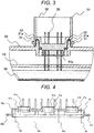
- FIG. 3 is a cross-sectional view of a main part of the electronic control device 1 according to the first embodiment of the present invention.
- the electronic control device 1 mainly includes a printed wiring board 10, a case 20, a cover 22, and three connectors 50 (50a to 50c).
- the case 20 protects the printed wiring board 10. At least three openings 21b, 21c, and 21d through which the connectors 50 are inserted are provided on a plane 20p of the case 20.
- the cover 22 seals an opening portion of the case 21 by being fixed to the case 21.
- the connector 50 is electrically connected to the printed wiring board 10.
- the seal material 30 waterproofs a space between an opening edge portion 20a of the case 20 and an inner surface of a peripheral edge portion 22b of the cover 22.
- a seal material 31 waterproofs a space between a housing groove 52 of the connector 50 and a plurality of convex portions 21a around the openings penetrating through the case 20.
- the printed wiring board 10 is fixed to the case 20 using screws 40.
- a heat dissipation adhesive 32 is interposed between the printed wiring board 10 and the case 20.
- the cover 22 is fixed to the case 20 using screws 41.
- the case 20 accommodates the printed wiring board 10 therein together with the cover 22, and protects the printed wiring board 10 to which the electronic components are mounted from water, foreign matters and the like.
- the case 20 is preferably made of metal, suitably aluminum, in order to dissipate heat generated by the electronic components and to shield noise.
- the case 20 is molded by an aluminum die-cast molding method using a metal mold.
- the material of the case 20 may be resin in the case of the electronic control device 1 configured of the electronic components that do not require heat dissipation or shielding.
- the case 20 is molded by an injection molding method.
- an outer shape of the case 20 has a size of 240 mm ⁇ 160 mm, which is relatively large in the electronic control device 1 disposed in an engine room, and has a rectangular shape.
- An electronic control device disclosed in PTL 1 generally has a size of about 160 mm ⁇ 160 mm, but the electronic control device 1 according to the present embodiment has a size which is 1.5 times of the size of the electronic control device disclosed in PTL 1 or larger.
- the three or more penetrating openings 21 are provided in the case 20.
- the third opening 21d is disposed outside of either the first opening 21b or the second opening between (in the middle of) the first opening 21b and the second opening 21c. That is, the third opening 21d is disposed at a position farthest from a center C of the plane 20p in the longitudinal direction of the case 20.
- the openings 21b, 21c, and 21d are rectangular and disposed so that long sides of the openings are parallel to each other. A distance from the center C of the plane 20p to a short side at the center C side of the first opening 21b is equal to a distance from the center C of the plane to a short side at the center C side of the second opening 21c.
- the opening 21 may be a hole through which the connector 50 is inserted or a hole through which a breathing filter is inserted.
- the opening 21 is a hole having a function of allowing the connector 50 to penetrate therethrough.
- the penetrating opening 21 is preferably provided at an outer side from the center of the case since pressure is applied inside the case 20 and a central portion of the case 20 is maximally deformed in an uneven direction under environment of transport and use of an automobile such as a change in altitude and a change in temperature.
- the opening 21d in the middle contributes to suppressing the deformation amount of the case by being disposed at the outermost side.
- Heat dissipation fins 23 to increase heat capacity are provided on the opposite side to a size where the openings 21 are disposed on an outer side surface of the case 20. As illustrated in FIG. 1 , an orientation of the heat dissipation fin 23 is parallel to the long side of the case 20, but may be parallel to the short side of the case 20. The orientation of the heat dissipation fin 23 are desirably parallel in a direction toward an overflow from a gate during molding by the aluminum die-cast molding method.
- the gate is provided on a surface (an upper surface or a side surface in contact with the short side) near the short side of the rectangular case 20 on the opposite side to the opening 21 so as to be parallel to a longitudinal direction of the connector 50 and the heat dissipation fin 23.
- the overflow is provided on a surface near the short side of the case 20 on the opposite side to the gate.
- the third opening 21d in the middle is provided at the outer side. Accordingly, a region 21e in which a space between the first opening 21b and the third opening 21d and a space between the second opening 21c and the third opening 21d overlap in the longitudinal direction is reduced as illustrated in FIG. 2 , and it is possible to suppress the deformation amount of the case and to improve the flow of hot water in the case.
- the gate is provided on a surface (an upper surface or a side surface in contact with the long side) near the long side of the rectangular case 20.
- the overflow is provided on a surface near the long side on the opposite side to the gate.
- the third opening 21d in the middle is provided at the outer side. Accordingly, the region 21e in which the space between the first opening 21b and the third opening 21d and the space between the second opening 21c and the third opening 21d overlap in the longitudinal direction is reduced, and it is possible to suppress the deformation amount of the case and to improve the flow of hot water in the case.
- the third opening 21d in the middle is formed to have a smaller area than the first opening 21b or the second opening 21c.
- at least one of a length 21g of the third opening 21d in the longitudinal direction and a width 21h (a length in a lateral direction) of the third opening is shortened with respect to the first opening 21b and the second opening 21c.
- a plurality of bases configured to fix the printed wiring board 10 are provided inside the case 20.
- a tapped base configured to fasten the screw 40 and a base with surface accuracy to which the heat dissipation adhesive 32 is applied are provided.
- a base which is fixed to the cover 22 via the screw 41 is also provided in the case 20.
- the electronic components and the like are mounted to the printed wiring board 10 using a conductive alloy such as solder. It is also possible to mount the electronic components and the like to both surfaces of the printed wiring board 10.
- the electronic components include passive components such as resistors and capacitors and active components such as semiconductors, and are mounted to the printed wiring board by a surface mounting method or an insertion mounting method. It is desirable to adopt electronic components with long service life that can withstand under the environment of the engine room for the automobile.
- a high-density ball grid array (BGA) and a quad for non-lead package (QFN) are mounted together with a quad flat package (QFP) as a package of the electronic components.
- the BGA has an electrode which is formed in a hemispherical shape by surface tension of a conductive alloy to terminal aligned in a grid pattern on a bottom surface of the package and is joined to the printed wiring board 10 by reflow.
- the QFN has a shorter terminal than the QFP and is connected to the printed wiring board 10 using a conductive alloy.
- the printed wiring board 10 is fixed to the tapped base of the case 20 together with the plurality of screws 40. At that time, the printed wiring board 10 and the base having the surface accuracy of the case 20 are fixed so as to sandwich the heat dissipation adhesive 32 therebetween. Since the size of the printed wiring board 10 is relatively large in the electronic control device 1 disposed in the engine room, the four or seven screws 40 are used for fixing.
- the respective screws are desirably disposed to have equal distances therebetween considering four corners of the printed wiring board 10 and the disposition of the electronic components.
- distortion occurs in the printed wiring board 10 near the screw 40. Therefore, it is desirable to provide the disposition in which there is no distortion in the connector 50, the BGA, and the joining portion of the QFN using the conductive alloy. That is, the screw 40 is not disposed near the connector 50 and the joining portion using the conductive alloy.
- the screw 40 has a function as a case ground and is electrically connected to the case 20 via the screw 40 and a GND wiring pattern of the printed wiring board 10. It is desirable for the case ground to be located at the four corners of the printed wiring board 10 in terms of routing of the wiring pattern of the printed wiring board 10.
- the printed wiring board 10 is preferably a glass epoxy board impregnated with epoxy resin on a cloth made of glass fiber superimposed.
- the printed wiring board 10 is a multilayered board in which an insulator and a pattern are stacked on each other and is a multilayered board of 4 layers to 6 layers since the high-density mounting is required therein.
- it is suitable to use a penetrating plate for wiring between the layers with a through hole that penetrates through the layers and a built-up plate formed by a build-up method.
- the heat dissipation adhesive 32 transfers the heat generated by the electronic component to the base having the surface accuracy of the case 20 through a via of the printed wiring board.
- a clearance between the case 20 and the printed wiring board 10 is widened, and thus, heat dissipation performance deteriorates. Therefore, it is effective to suppress the deformation of the case 20 in order to maintain the heat dissipation performance.
- the heat-generating electronic component that needs to dissipate heat is disposed under the heat dissipation fin 23.
- the connector 50 is configured of a housing 51, a terminal 53, and a potting material 51p.
- the terminal 53 is press-molded with a copper-based material having high thermal conductivity.
- a shape of the terminal 53 is a straight line, and s tip end thereof is crushed so as to be easily invited to the connector on a harness side or the through hole of the printed wiring board.
- the housing 51 is molded using resin by an injection molding method, and the terminal 53 is press-fitted thereto.
- the housing 51 may be molded by an insertion molding method so that the terminal 53 and the resin are integrated.
- the potting material 51p is provided in order to airtight a gap between the housing 51 and the terminal 53.
- the size of the connector 50 depends on the number of poles of the terminal 53 and the width of the terminal 53, and the length 21g in the longitudinal direction and the width 21h of the opening illustrated in FIG. 2 are determined.
- the terminal 53 has about 60 to 80 poles in total including a signal system terminal and a power system terminal together with a difference in current capacity.
- the power system terminal is wider.
- the terminal 53 and the penetrating through hole of the printed wiring board 10 are connected using a conductive alloy (not illustrated) such as solder.
- a press-fit terminal (not illustrated) may be used as the terminal 53, and the terminal 53 and the printed wiring board 10 may be mechanically and electrically connected.
- the third connector 50c among the three connectors 50 is provided between the first connector 50a and the second connector 50b. Similarly to the opening 21 of the case, the third connector 50c in the middle is disposed on the outermost side. Although there are three connectors in the present embodiment, the number of connectors is not limited to three, and three or more connectors may be used. Accordingly, the number of the openings 21 of the case becomes three or more. When the third connector 50c is disposed on the outermost side, it is possible to increase the area for mounting the electronic components. In addition, the wiring pattern of the printed wiring board 10 does not have high density, and it is also possible to avoid the wiring overlap of the pattern wiring.
- the connector 50 is connected to the case 20 from the outer surface side of the case 20 via the seal material 31 on the outer surface side of the case 20, and the terminal 53 is connected to the printed wiring board 10.
- the terminal 53 may be first connected to the printed wiring board 10, and then, the connector 50 may be connected to the case 20 from an inner surface side of the case 20 via the seal material 31 on the inner surface side of the case 20.
- connection of the connector 50 from the outside of the case 20 has an advantage that it is possible to miniaturize the seal structure of the connector 50.
- a housing groove 52 in which the seal material 31 is embedded is provided around a bottom of the housing 51 of the connector 50.
- the housing groove 52 is fitted to the convex portion 21a around the opening 21 of the case 20.
- a labyrinth structure is formed using a depth of the housing groove 52 and a height of the convex portion 21a of the opening 21 of the case 20 to protect the electronic components from foreign matters such as salt water so as to satisfy a condition required by the environmental specification of the engine room. Since the seal material 31 is filled in the clearance between the housing groove 52 and the convex portion 21a of the opening 21 of the case 20, the clearance and the amount of the seal material 31 are determined in consideration of an assembling error.
- the seal material 31 functions as a buffer material. Since the clearance is small, however, when the deformation occurs in the case 20 exceeding the function as the buffer material, the connector 50 also deforms at the same time. The deformation of the connector 50 also affects the terminal 53, and the deformation is also transmitted to the printed wiring board 10 via the conductive adhesive at the same time.
- the seal material 31 is preferably a silicone adhesive having heat resistance, water resistance, chemical resistance, and flexibility in order to protect the electronic components from the foreign matters such as salt water.
- a peripheral edge portion 22b is provided on the entire inner periphery of the cover 22.
- a seal material 30 is applied between the peripheral edge portion 22b of the cover 22 and the opening edge portion 20a of the case 20 to protect the electronic components from the foreign matters such as salt water.
- An iron-based or aluminum-based steel plate is preferably used as the material of the cover 22, but resin or aluminum die-cast may be used.
- the cover 22 is made of metal, influence of an electromagnetic wave is not applied to the outside. In addition, there is less influence of the electromagnetic wave than the case of using other materials.
- the seal material 30 is preferably a silicon adhesive.
- the seal material 30 is configured to have an adhesive force capable of withstanding deformation.
- the cover 22 holes through which the screws 41 to be fixed to the case 20 penetrate are provided at four corners.
- the cover 22 and the case 20 are fixed by the screws 41, together with the seal material 30. It is desirable to dispose the screws 41 at the four corners of the cover 22 so that an application trajectory of the seal material 30 is not complicated. Since the size of the electronic control device is 1.5 times larger than that of the conventional electronic control device in the present embodiment, the thin material is selected as the cover 22, and ribs, dimples, steps and the like are provided to secure the strength.
- FIG. 4 is a cross-sectional view of a main part of a case of the electronic control device 1 according to the second embodiment of the present invention.
- a wall thickness of the case 20 serving as a reference is a wall thickness 24.
- a wall thickness between the first opening 21b and the third opening 21d and a wall thickness between the second opening 21c and the third opening 21d are a wall thickness 24a.
- the wall thickness 24a is larger than the wall thickness 24 serving as the reference.
- a thickness of the case 20 in a first region between the first opening 21b and the third opening 21d and a thickness of the case 20 in a second region between the second opening 21c and the third opening 21d are larger than a thickness of a third region excluding the first region and the second region in the plane 20p.
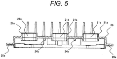
- FIG. 5 is a cross-sectional view of a main part of a case of the electronic control device 1 according to the third embodiment of the present invention.
- ribs 24b are provided between the first opening 21b and the third opening 21d and between the second opening 21c and the third opening 21d in the case 20.
- the ribs 24b may be provided inside or outside the case 20.
- the rib 24b has a height not to interfere with the electronic component.
- a large and tall electronic component is not generally disposed, so that it is possible to avoid interference.
- the rib 24b is provided outside the case 20, it is difficult to make the height of the rib 24b high since a female connector on a vehicle side to be fitted to the connector 50 is assembled. Therefore, it is preferable to dispose the rib 24b inside the case 20.
- FIG. 6 is a front view of a main part of a case of the electronic control device 1 according to the fourth embodiment of the present invention.
- an extension portion 23a obtained by extending the heat dissipation fin 23 is provided between the first opening 21b and the third opening 21d and between the second opening 21c and the third opening 21d in the case 20. Since a female connector on a vehicle side to be fitted to the connector 50 is assembled, a height of the extension portion 23a is set to a height that does not interfere with the female connector. That is, the height of the extension portion 23a is lower than the height of the heat dissipation fin 23.
- FIG. 7 is a front view of a main part of a case of the electronic control device 1 according to the fifth embodiment of the present invention. As illustrated in FIG. 7 , an extension portion 23b obtained by extending the heat dissipation fin 23 is provided in a region 20fs formed by disposing the third opening 21d in which the deformation amount of the case 20 is the largest on the outer side.
- the case 20 is provided with the extension portion 23b obtained by extending the heat dissipation fin 23 to the front side of a short side of the third opening 21d on the center C side of the plane 20p.
- a height of the extension portion 23b is the same as that of the heat dissipation fin 23.
- the sectional area of the periphery of the third opening 21d in which the deformation amount of the case 20 is the largest increases, and it is possible to increase the strength and to suppress the deformation amount in the periphery of the third opening 21d and the region 21e overlapping in the longitudinal direction. It is possible to cause the hot water to flow to the extension portion 23b simultaneously to the heat dissipation fin 23 during the aluminum die-cast molding by extending the heat dissipation fin 23, and thus, the flow of hot water becomes favorable.
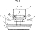
- FIG. 8 is a cross-sectional view of a main part of a case of the electronic control device 1 according to the sixth embodiment of the present invention.
- a V-shaped groove 25 (a groove having a V-shaped cross section) is provided between the first opening 21b and the third opening 21d or between the second opening 21c and the third opening 21d in the case 20.
- the salt water or the foreign matters can be drained without stopping in the periphery of the seal material 31, and it is possible to prevent corrosion of the seal material 31 and to protect adhesion reliability for a long term.
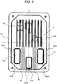
- FIG. 9 is a view for describing a modification of the case 20 of the electronic control device 1 according to the sixth embodiment of the present invention.
- the case 20 has a slope (part indicated by a frame line 20s1) in contact with a long side opposing a long side of the first opening 21b on the center C side of the plane 20p and a slope (part indicated by a frame line 20s2) in contact with a short side opposing a short side of the first opening 21b on the center C side of the plane 20p.
- case 20 has a slope (part indicated by a frame line 20s3) in contact with a long side opposed to a long side of the second opening 21c on the center C side of the plane 20p, and a slope (part indicated by a frame line 20s4) in contact with a short side opposing a short side of the second opening 21c on the center C side of the plane 20p.
- case 20 has a slope (part indicated by a frame line 20s5) in contact with a short side opposing a short side of the third opening 21d on the center C side of the plane 20p.
- the present invention is not limited to the above-described embodiments, and includes various modification examples.
- the above-described embodiments have been described in detail in order to describe the present invention in an easily understandable manner, and are not necessarily limited to one including the entire configuration that has been described above.
- some configurations of a certain embodiment can be substituted by configurations of another embodiment, and further, a configuration of another embodiment can be added to a configuration of a certain embodiment.
- addition, deletion or substitution of other configurations can be made with respect to some configurations of each embodiment.
Landscapes
- Engineering & Computer Science (AREA)
- Microelectronics & Electronic Packaging (AREA)
- Mechanical Engineering (AREA)
- Architecture (AREA)
- Civil Engineering (AREA)
- Structural Engineering (AREA)
- Physics & Mathematics (AREA)
- Thermal Sciences (AREA)
- Casings For Electric Apparatus (AREA)
- Connection Or Junction Boxes (AREA)
- Cooling Or The Like Of Electrical Apparatus (AREA)
Applications Claiming Priority (2)
| Application Number | Priority Date | Filing Date | Title |
|---|---|---|---|
| JP2015004948 | 2015-01-14 | ||
| PCT/JP2016/050421 WO2016114221A1 (ja) | 2015-01-14 | 2016-01-08 | 電子制御装置 |
Publications (3)
| Publication Number | Publication Date |
|---|---|
| EP3247013A1 true EP3247013A1 (de) | 2017-11-22 |
| EP3247013A4 EP3247013A4 (de) | 2018-08-15 |
| EP3247013B1 EP3247013B1 (de) | 2021-03-10 |
Family
ID=56405768
Family Applications (1)
| Application Number | Title | Priority Date | Filing Date |
|---|---|---|---|
| EP16737292.9A Active EP3247013B1 (de) | 2015-01-14 | 2016-01-08 | Elektronische steuerungsvorrichtung |
Country Status (5)
| Country | Link |
|---|---|
| US (2) | US10821921B2 (de) |
| EP (1) | EP3247013B1 (de) |
| JP (1) | JP6302093B2 (de) |
| CN (1) | CN107112736B (de) |
| WO (1) | WO2016114221A1 (de) |
Cited By (1)
| Publication number | Priority date | Publication date | Assignee | Title |
|---|---|---|---|---|
| US20200015372A1 (en) * | 2017-05-04 | 2020-01-09 | Bayerische Motoren Werke Aktiengesellschaft | Electronic Module |
Families Citing this family (20)
| Publication number | Priority date | Publication date | Assignee | Title |
|---|---|---|---|---|
| JP6218955B2 (ja) * | 2014-09-24 | 2017-10-25 | 三菱電機株式会社 | 車両用電子制御装置及びモータ駆動装置 |
| USD821446S1 (en) * | 2016-08-31 | 2018-06-26 | Sevcon Limited | Electric motor controller |
| JP2018074793A (ja) * | 2016-10-31 | 2018-05-10 | ミネベアミツミ株式会社 | モータ |
| JP6645413B2 (ja) * | 2016-12-15 | 2020-02-14 | 豊田合成株式会社 | 電子装置 |
| JP2018137174A (ja) * | 2017-02-23 | 2018-08-30 | オムロン株式会社 | 電子機器 |
| US10243290B2 (en) * | 2017-07-17 | 2019-03-26 | Rohde & Schwarz Gmbh & Co. Kg | Electric connector, printed circuit board and production method |
| JP6546239B2 (ja) * | 2017-10-05 | 2019-07-17 | ファナック株式会社 | 電子装置 |
| JP7064601B2 (ja) * | 2018-09-03 | 2022-05-10 | 日立Astemo株式会社 | 電子制御装置 |
| JP6871227B2 (ja) * | 2018-12-27 | 2021-05-12 | 矢崎総業株式会社 | 防水パッキン、防水コネクタ、及びワイヤハーネス |
| US10945347B2 (en) * | 2018-12-27 | 2021-03-09 | lonQ, Inc. | Techniques for making hermetic feedthroughs for enclosures |
| EP3927583A4 (de) * | 2019-02-18 | 2022-12-14 | Arens Controls Company, LLC | Stromverteilungsanordnung |
| JP7257893B2 (ja) * | 2019-06-25 | 2023-04-14 | 日立Astemo株式会社 | 電子制御装置 |
| DE102019219478A1 (de) * | 2019-12-12 | 2021-06-17 | Continental Automotive Gmbh | Modular erweiterbares elektronisches steuergerät |
| US11881673B2 (en) * | 2020-02-27 | 2024-01-23 | Amtrol Licensing Inc. | Electrical cover for wired devices |
| USD942392S1 (en) * | 2020-04-30 | 2022-02-01 | Thermo King Corporation | High power module for controller of transport climate control system |
| USD944199S1 (en) * | 2020-04-30 | 2022-02-22 | Thermo King Corporation | Low power module for controller of transport climate control system |
| CN116636312A (zh) * | 2021-03-10 | 2023-08-22 | 日立安斯泰莫株式会社 | 电子控制装置 |
| JP7681635B2 (ja) * | 2023-03-30 | 2025-05-22 | 双葉電子工業株式会社 | 電子機器及び電子機器の製造方法 |
| EP4446086A1 (de) * | 2023-04-13 | 2024-10-16 | WWS Technik in Form und Kunststoff GmbH | Gehäuseschale und kunststoffspritzgussverfahren zur herstellung eines elektrischen verteilers mit einer gehäuseschale |
| USD1110970S1 (en) * | 2024-04-02 | 2026-02-03 | Epec Oy | Casing for control device |
Family Cites Families (31)
| Publication number | Priority date | Publication date | Assignee | Title |
|---|---|---|---|---|
| US3601661A (en) * | 1970-02-02 | 1971-08-24 | Westinghouse Air Brake Co | Finned modular electrical equipment package with mounting bracket |
| US5067905A (en) * | 1989-06-09 | 1991-11-26 | Yazaki Corporation | Electric connection box |
| JP3212210B2 (ja) * | 1994-02-25 | 2001-09-25 | タイコエレクトロニクスアンプ株式会社 | カム部材付きコネクタ |
| US5761042A (en) * | 1996-10-02 | 1998-06-02 | Motorola, Inc. | Radio frequency compatible multi-board cluster |
| JP3356045B2 (ja) * | 1998-01-26 | 2002-12-09 | 住友電装株式会社 | ハーネスカバー及び電気接続箱 |
| JP2000005860A (ja) * | 1998-06-22 | 2000-01-11 | Toshiba Corp | 金型装置及び電子機器用筐体の製造方法 |
| JP3405249B2 (ja) * | 1999-02-01 | 2003-05-12 | 住友電装株式会社 | 電気接続箱 |
| JP2001237557A (ja) * | 2000-02-24 | 2001-08-31 | Keihin Corp | 電子回路基板の収容ケース |
| US6350949B1 (en) * | 2000-06-23 | 2002-02-26 | Tyco Electronics Corp | Sealed power distribution module |
| JP2002058130A (ja) * | 2000-08-07 | 2002-02-22 | Sumitomo Wiring Syst Ltd | 電気接続箱 |
| JP2002078144A (ja) * | 2000-08-24 | 2002-03-15 | Sumitomo Wiring Syst Ltd | 電気接続箱 |
| JP3977609B2 (ja) * | 2001-04-27 | 2007-09-19 | 矢崎総業株式会社 | 電気接続箱 |
| US20030035278A1 (en) * | 2001-08-14 | 2003-02-20 | Lawlyes Daniel A. | Partitioned circuit assembly |
| US6652292B2 (en) * | 2002-02-22 | 2003-11-25 | Molex Incorporated | Electrical connector assembly incorporating printed circuit board |
| JP3954915B2 (ja) * | 2002-05-29 | 2007-08-08 | 矢崎総業株式会社 | 電気接続箱とその製造方法 |
| JP2004032839A (ja) * | 2002-06-21 | 2004-01-29 | Sumitomo Wiring Syst Ltd | 電気接続箱 |
| US7396254B2 (en) * | 2006-05-15 | 2008-07-08 | Deere & Company | Flexible electrical connector/housing assembly |
| WO2008005945A2 (en) | 2006-06-30 | 2008-01-10 | Molex Incorporated | Compliant pin control module and method for making the same |
| JP4887273B2 (ja) * | 2007-12-27 | 2012-02-29 | 日立オートモティブシステムズ株式会社 | 電子制御装置 |
| US7867023B2 (en) * | 2008-04-08 | 2011-01-11 | Molex Incorporated | Electrical connector having positioning peg and assembly having same |
| JP2009253231A (ja) | 2008-04-10 | 2009-10-29 | Fujitsu Ten Ltd | 電子機器 |
| WO2010027504A1 (en) * | 2008-09-08 | 2010-03-11 | Materials And Electrochemical Research (Mer) Corporation | Machinable metal/diamond metal matrix composite compound structure and method of making same |
| JP5392243B2 (ja) * | 2010-12-14 | 2014-01-22 | 株式会社デンソー | 電子装置およびその製造方法 |
| US8523581B2 (en) | 2011-04-29 | 2013-09-03 | Tyco Electronics Corporation | Header connector assembly |
| EP3410832B1 (de) * | 2011-09-26 | 2020-09-09 | Autonetworks Technologies, Ltd. | Stromverteilerkasten |
| CN103023279B (zh) * | 2011-09-27 | 2015-05-13 | 株式会社京浜 | 半导体控制装置 |
| DE102012204145A1 (de) * | 2012-03-16 | 2013-09-19 | Continental Automotive Gmbh | Gehäuseblende zur Aufnahme von Steckermodulen |
| JP5499125B2 (ja) | 2012-09-19 | 2014-05-21 | 三菱電機株式会社 | 筐体及びその筐体の組立方法 |
| US8952562B2 (en) * | 2012-09-20 | 2015-02-10 | Komatsu Ltd. | Controller mounted in construction machine |
| ITVR20130255A1 (it) * | 2013-11-25 | 2015-05-26 | Gianfranco Natali | Parte di contenitore per apparecchiature elettroniche avente funzione di dissipatore di calore e metodo per la sua realizzazione |
| JP5943985B2 (ja) * | 2014-10-30 | 2016-07-05 | 三菱電機株式会社 | 電子制御装置 |
-
2016
- 2016-01-08 JP JP2016569338A patent/JP6302093B2/ja active Active
- 2016-01-08 US US15/535,861 patent/US10821921B2/en active Active
- 2016-01-08 EP EP16737292.9A patent/EP3247013B1/de active Active
- 2016-01-08 CN CN201680004332.4A patent/CN107112736B/zh active Active
- 2016-01-08 WO PCT/JP2016/050421 patent/WO2016114221A1/ja not_active Ceased
-
2020
- 2020-03-26 US US16/831,394 patent/US11370372B2/en active Active
Cited By (2)
| Publication number | Priority date | Publication date | Assignee | Title |
|---|---|---|---|---|
| US20200015372A1 (en) * | 2017-05-04 | 2020-01-09 | Bayerische Motoren Werke Aktiengesellschaft | Electronic Module |
| US10939567B2 (en) * | 2017-05-04 | 2021-03-02 | Bayerische Motoren Werke Aktiengesellschaft | Electronic module using board lacquer to reinforce the circuit board to the unit housing |
Also Published As
| Publication number | Publication date |
|---|---|
| US10821921B2 (en) | 2020-11-03 |
| US20200223382A1 (en) | 2020-07-16 |
| EP3247013A4 (de) | 2018-08-15 |
| WO2016114221A1 (ja) | 2016-07-21 |
| CN107112736B (zh) | 2018-09-21 |
| EP3247013B1 (de) | 2021-03-10 |
| US11370372B2 (en) | 2022-06-28 |
| CN107112736A (zh) | 2017-08-29 |
| JP6302093B2 (ja) | 2018-03-28 |
| JPWO2016114221A1 (ja) | 2017-09-21 |
| US20170334375A1 (en) | 2017-11-23 |
Similar Documents
| Publication | Publication Date | Title |
|---|---|---|
| US11370372B2 (en) | Electronic control device | |
| JP6488391B2 (ja) | 車載制御装置 | |
| JP6542642B2 (ja) | 電子制御装置 | |
| US7924572B2 (en) | Control device and method of manufacturing thereof | |
| KR100755093B1 (ko) | 제어장치 및 납땜방법 | |
| US7578681B2 (en) | Electronic device including printed circuit board and electronic element mounted on the printed circuit board | |
| JP6634316B2 (ja) | 樹脂封止型車載制御装置 | |
| EP2164312A1 (de) | Elektrogeräteinheit | |
| US8530759B2 (en) | Electronic apparatus | |
| US20140045386A1 (en) | Connector and Manufacturing Method Thereof | |
| JP4291215B2 (ja) | 電子機器の密閉筐体 | |
| JP5929958B2 (ja) | 電子装置 | |
| JP5939895B2 (ja) | 車載用電子制御装置 | |
| JP6307871B2 (ja) | 電子制御装置 | |
| JP5066897B2 (ja) | 電装品ユニット | |
| KR102485123B1 (ko) | 이미지 센서 어셈블리 | |
| JP3457296B2 (ja) | 電子機器用筐体 | |
| JP6698563B2 (ja) | 電子制御装置 | |
| CN121174425A (zh) | 一种用于极端应力环境的电子组件结构 |
Legal Events
| Date | Code | Title | Description |
|---|---|---|---|
| STAA | Information on the status of an ep patent application or granted ep patent |
Free format text: STATUS: THE INTERNATIONAL PUBLICATION HAS BEEN MADE |
|
| PUAI | Public reference made under article 153(3) epc to a published international application that has entered the european phase |
Free format text: ORIGINAL CODE: 0009012 |
|
| STAA | Information on the status of an ep patent application or granted ep patent |
Free format text: STATUS: REQUEST FOR EXAMINATION WAS MADE |
|
| 17P | Request for examination filed |
Effective date: 20170814 |
|
| AK | Designated contracting states |
Kind code of ref document: A1 Designated state(s): AL AT BE BG CH CY CZ DE DK EE ES FI FR GB GR HR HU IE IS IT LI LT LU LV MC MK MT NL NO PL PT RO RS SE SI SK SM TR |
|
| AX | Request for extension of the european patent |
Extension state: BA ME |
|
| DAV | Request for validation of the european patent (deleted) | ||
| DAX | Request for extension of the european patent (deleted) | ||
| A4 | Supplementary search report drawn up and despatched |
Effective date: 20180716 |
|
| RIC1 | Information provided on ipc code assigned before grant |
Ipc: B60R 16/02 20060101ALI20180710BHEP Ipc: H05K 5/00 20060101ALI20180710BHEP Ipc: H02G 3/16 20060101AFI20180710BHEP Ipc: H01R 13/518 20060101ALI20180710BHEP |
|
| STAA | Information on the status of an ep patent application or granted ep patent |
Free format text: STATUS: EXAMINATION IS IN PROGRESS |
|
| 17Q | First examination report despatched |
Effective date: 20190522 |
|
| GRAP | Despatch of communication of intention to grant a patent |
Free format text: ORIGINAL CODE: EPIDOSNIGR1 |
|
| STAA | Information on the status of an ep patent application or granted ep patent |
Free format text: STATUS: GRANT OF PATENT IS INTENDED |
|
| INTG | Intention to grant announced |
Effective date: 20201019 |
|
| GRAS | Grant fee paid |
Free format text: ORIGINAL CODE: EPIDOSNIGR3 |
|
| GRAA | (expected) grant |
Free format text: ORIGINAL CODE: 0009210 |
|
| STAA | Information on the status of an ep patent application or granted ep patent |
Free format text: STATUS: THE PATENT HAS BEEN GRANTED |
|
| AK | Designated contracting states |
Kind code of ref document: B1 Designated state(s): AL AT BE BG CH CY CZ DE DK EE ES FI FR GB GR HR HU IE IS IT LI LT LU LV MC MK MT NL NO PL PT RO RS SE SI SK SM TR |
|
| REG | Reference to a national code |
Ref country code: GB Ref legal event code: FG4D |
|
| REG | Reference to a national code |
Ref country code: AT Ref legal event code: REF Ref document number: 1370872 Country of ref document: AT Kind code of ref document: T Effective date: 20210315 Ref country code: CH Ref legal event code: EP |
|
| REG | Reference to a national code |
Ref country code: IE Ref legal event code: FG4D |
|
| REG | Reference to a national code |
Ref country code: DE Ref legal event code: R096 Ref document number: 602016054003 Country of ref document: DE |
|
| REG | Reference to a national code |
Ref country code: LT Ref legal event code: MG9D |
|
| PG25 | Lapsed in a contracting state [announced via postgrant information from national office to epo] |
Ref country code: GR Free format text: LAPSE BECAUSE OF FAILURE TO SUBMIT A TRANSLATION OF THE DESCRIPTION OR TO PAY THE FEE WITHIN THE PRESCRIBED TIME-LIMIT Effective date: 20210611 Ref country code: HR Free format text: LAPSE BECAUSE OF FAILURE TO SUBMIT A TRANSLATION OF THE DESCRIPTION OR TO PAY THE FEE WITHIN THE PRESCRIBED TIME-LIMIT Effective date: 20210310 Ref country code: FI Free format text: LAPSE BECAUSE OF FAILURE TO SUBMIT A TRANSLATION OF THE DESCRIPTION OR TO PAY THE FEE WITHIN THE PRESCRIBED TIME-LIMIT Effective date: 20210310 Ref country code: NO Free format text: LAPSE BECAUSE OF FAILURE TO SUBMIT A TRANSLATION OF THE DESCRIPTION OR TO PAY THE FEE WITHIN THE PRESCRIBED TIME-LIMIT Effective date: 20210610 Ref country code: BG Free format text: LAPSE BECAUSE OF FAILURE TO SUBMIT A TRANSLATION OF THE DESCRIPTION OR TO PAY THE FEE WITHIN THE PRESCRIBED TIME-LIMIT Effective date: 20210610 Ref country code: LT Free format text: LAPSE BECAUSE OF FAILURE TO SUBMIT A TRANSLATION OF THE DESCRIPTION OR TO PAY THE FEE WITHIN THE PRESCRIBED TIME-LIMIT Effective date: 20210310 |
|
| REG | Reference to a national code |
Ref country code: AT Ref legal event code: MK05 Ref document number: 1370872 Country of ref document: AT Kind code of ref document: T Effective date: 20210310 |
|
| REG | Reference to a national code |
Ref country code: NL Ref legal event code: MP Effective date: 20210310 |
|
| PG25 | Lapsed in a contracting state [announced via postgrant information from national office to epo] |
Ref country code: SE Free format text: LAPSE BECAUSE OF FAILURE TO SUBMIT A TRANSLATION OF THE DESCRIPTION OR TO PAY THE FEE WITHIN THE PRESCRIBED TIME-LIMIT Effective date: 20210310 Ref country code: LV Free format text: LAPSE BECAUSE OF FAILURE TO SUBMIT A TRANSLATION OF THE DESCRIPTION OR TO PAY THE FEE WITHIN THE PRESCRIBED TIME-LIMIT Effective date: 20210310 Ref country code: RS Free format text: LAPSE BECAUSE OF FAILURE TO SUBMIT A TRANSLATION OF THE DESCRIPTION OR TO PAY THE FEE WITHIN THE PRESCRIBED TIME-LIMIT Effective date: 20210310 |
|
| REG | Reference to a national code |
Ref country code: DE Ref legal event code: R081 Ref document number: 602016054003 Country of ref document: DE Owner name: HITACHI ASTEMO, LTD., HITACHINAKA-SHI, JP Free format text: FORMER OWNER: HITACHI AUTOMOTIVE SYSTEMS, LTD., HITACHINAKA-SHI, IBARAKI, JP |
|
| RAP4 | Party data changed (patent owner data changed or rights of a patent transferred) |
Owner name: HITACHI ASTEMO, LTD. |
|
| PG25 | Lapsed in a contracting state [announced via postgrant information from national office to epo] |
Ref country code: NL Free format text: LAPSE BECAUSE OF FAILURE TO SUBMIT A TRANSLATION OF THE DESCRIPTION OR TO PAY THE FEE WITHIN THE PRESCRIBED TIME-LIMIT Effective date: 20210310 |
|
| PG25 | Lapsed in a contracting state [announced via postgrant information from national office to epo] |
Ref country code: CZ Free format text: LAPSE BECAUSE OF FAILURE TO SUBMIT A TRANSLATION OF THE DESCRIPTION OR TO PAY THE FEE WITHIN THE PRESCRIBED TIME-LIMIT Effective date: 20210310 Ref country code: EE Free format text: LAPSE BECAUSE OF FAILURE TO SUBMIT A TRANSLATION OF THE DESCRIPTION OR TO PAY THE FEE WITHIN THE PRESCRIBED TIME-LIMIT Effective date: 20210310 Ref country code: SM Free format text: LAPSE BECAUSE OF FAILURE TO SUBMIT A TRANSLATION OF THE DESCRIPTION OR TO PAY THE FEE WITHIN THE PRESCRIBED TIME-LIMIT Effective date: 20210310 Ref country code: AT Free format text: LAPSE BECAUSE OF FAILURE TO SUBMIT A TRANSLATION OF THE DESCRIPTION OR TO PAY THE FEE WITHIN THE PRESCRIBED TIME-LIMIT Effective date: 20210310 |
|
| PG25 | Lapsed in a contracting state [announced via postgrant information from national office to epo] |
Ref country code: IS Free format text: LAPSE BECAUSE OF FAILURE TO SUBMIT A TRANSLATION OF THE DESCRIPTION OR TO PAY THE FEE WITHIN THE PRESCRIBED TIME-LIMIT Effective date: 20210710 Ref country code: PT Free format text: LAPSE BECAUSE OF FAILURE TO SUBMIT A TRANSLATION OF THE DESCRIPTION OR TO PAY THE FEE WITHIN THE PRESCRIBED TIME-LIMIT Effective date: 20210712 Ref country code: PL Free format text: LAPSE BECAUSE OF FAILURE TO SUBMIT A TRANSLATION OF THE DESCRIPTION OR TO PAY THE FEE WITHIN THE PRESCRIBED TIME-LIMIT Effective date: 20210310 Ref country code: SK Free format text: LAPSE BECAUSE OF FAILURE TO SUBMIT A TRANSLATION OF THE DESCRIPTION OR TO PAY THE FEE WITHIN THE PRESCRIBED TIME-LIMIT Effective date: 20210310 Ref country code: RO Free format text: LAPSE BECAUSE OF FAILURE TO SUBMIT A TRANSLATION OF THE DESCRIPTION OR TO PAY THE FEE WITHIN THE PRESCRIBED TIME-LIMIT Effective date: 20210310 |
|
| REG | Reference to a national code |
Ref country code: DE Ref legal event code: R097 Ref document number: 602016054003 Country of ref document: DE |
|
| PLBE | No opposition filed within time limit |
Free format text: ORIGINAL CODE: 0009261 |
|
| STAA | Information on the status of an ep patent application or granted ep patent |
Free format text: STATUS: NO OPPOSITION FILED WITHIN TIME LIMIT |
|
| PG25 | Lapsed in a contracting state [announced via postgrant information from national office to epo] |
Ref country code: DK Free format text: LAPSE BECAUSE OF FAILURE TO SUBMIT A TRANSLATION OF THE DESCRIPTION OR TO PAY THE FEE WITHIN THE PRESCRIBED TIME-LIMIT Effective date: 20210310 Ref country code: AL Free format text: LAPSE BECAUSE OF FAILURE TO SUBMIT A TRANSLATION OF THE DESCRIPTION OR TO PAY THE FEE WITHIN THE PRESCRIBED TIME-LIMIT Effective date: 20210310 Ref country code: ES Free format text: LAPSE BECAUSE OF FAILURE TO SUBMIT A TRANSLATION OF THE DESCRIPTION OR TO PAY THE FEE WITHIN THE PRESCRIBED TIME-LIMIT Effective date: 20210310 |
|
| 26N | No opposition filed |
Effective date: 20211213 |
|
| PG25 | Lapsed in a contracting state [announced via postgrant information from national office to epo] |
Ref country code: SI Free format text: LAPSE BECAUSE OF FAILURE TO SUBMIT A TRANSLATION OF THE DESCRIPTION OR TO PAY THE FEE WITHIN THE PRESCRIBED TIME-LIMIT Effective date: 20210310 |
|
| PG25 | Lapsed in a contracting state [announced via postgrant information from national office to epo] |
Ref country code: IT Free format text: LAPSE BECAUSE OF FAILURE TO SUBMIT A TRANSLATION OF THE DESCRIPTION OR TO PAY THE FEE WITHIN THE PRESCRIBED TIME-LIMIT Effective date: 20210310 |
|
| PG25 | Lapsed in a contracting state [announced via postgrant information from national office to epo] |
Ref country code: IS Free format text: LAPSE BECAUSE OF FAILURE TO SUBMIT A TRANSLATION OF THE DESCRIPTION OR TO PAY THE FEE WITHIN THE PRESCRIBED TIME-LIMIT Effective date: 20210710 |
|
| PG25 | Lapsed in a contracting state [announced via postgrant information from national office to epo] |
Ref country code: MC Free format text: LAPSE BECAUSE OF FAILURE TO SUBMIT A TRANSLATION OF THE DESCRIPTION OR TO PAY THE FEE WITHIN THE PRESCRIBED TIME-LIMIT Effective date: 20210310 |
|
| REG | Reference to a national code |
Ref country code: CH Ref legal event code: PL |
|
| GBPC | Gb: european patent ceased through non-payment of renewal fee |
Effective date: 20220108 |
|
| REG | Reference to a national code |
Ref country code: BE Ref legal event code: MM Effective date: 20220131 |
|
| PG25 | Lapsed in a contracting state [announced via postgrant information from national office to epo] |
Ref country code: LU Free format text: LAPSE BECAUSE OF NON-PAYMENT OF DUE FEES Effective date: 20220108 Ref country code: GB Free format text: LAPSE BECAUSE OF NON-PAYMENT OF DUE FEES Effective date: 20220108 |
|
| PG25 | Lapsed in a contracting state [announced via postgrant information from national office to epo] |
Ref country code: FR Free format text: LAPSE BECAUSE OF NON-PAYMENT OF DUE FEES Effective date: 20220131 Ref country code: BE Free format text: LAPSE BECAUSE OF NON-PAYMENT OF DUE FEES Effective date: 20220131 |
|
| PG25 | Lapsed in a contracting state [announced via postgrant information from national office to epo] |
Ref country code: LI Free format text: LAPSE BECAUSE OF NON-PAYMENT OF DUE FEES Effective date: 20220131 Ref country code: CH Free format text: LAPSE BECAUSE OF NON-PAYMENT OF DUE FEES Effective date: 20220131 |
|
| PG25 | Lapsed in a contracting state [announced via postgrant information from national office to epo] |
Ref country code: IE Free format text: LAPSE BECAUSE OF NON-PAYMENT OF DUE FEES Effective date: 20220108 |
|
| PG25 | Lapsed in a contracting state [announced via postgrant information from national office to epo] |
Ref country code: HU Free format text: LAPSE BECAUSE OF FAILURE TO SUBMIT A TRANSLATION OF THE DESCRIPTION OR TO PAY THE FEE WITHIN THE PRESCRIBED TIME-LIMIT; INVALID AB INITIO Effective date: 20160108 |
|
| PG25 | Lapsed in a contracting state [announced via postgrant information from national office to epo] |
Ref country code: MK Free format text: LAPSE BECAUSE OF FAILURE TO SUBMIT A TRANSLATION OF THE DESCRIPTION OR TO PAY THE FEE WITHIN THE PRESCRIBED TIME-LIMIT Effective date: 20210310 Ref country code: CY Free format text: LAPSE BECAUSE OF FAILURE TO SUBMIT A TRANSLATION OF THE DESCRIPTION OR TO PAY THE FEE WITHIN THE PRESCRIBED TIME-LIMIT Effective date: 20210310 |
|
| PG25 | Lapsed in a contracting state [announced via postgrant information from national office to epo] |
Ref country code: TR Free format text: LAPSE BECAUSE OF FAILURE TO SUBMIT A TRANSLATION OF THE DESCRIPTION OR TO PAY THE FEE WITHIN THE PRESCRIBED TIME-LIMIT Effective date: 20210310 |
|
| PG25 | Lapsed in a contracting state [announced via postgrant information from national office to epo] |
Ref country code: MT Free format text: LAPSE BECAUSE OF FAILURE TO SUBMIT A TRANSLATION OF THE DESCRIPTION OR TO PAY THE FEE WITHIN THE PRESCRIBED TIME-LIMIT Effective date: 20210310 |
|
| PGFP | Annual fee paid to national office [announced via postgrant information from national office to epo] |
Ref country code: DE Payment date: 20251203 Year of fee payment: 11 |