EP3248936A1 - Structure d'intégration de capteur de pression mems et de capteur inertiel mems - Google Patents
Structure d'intégration de capteur de pression mems et de capteur inertiel mems Download PDFInfo
- Publication number
- EP3248936A1 EP3248936A1 EP15894015.5A EP15894015A EP3248936A1 EP 3248936 A1 EP3248936 A1 EP 3248936A1 EP 15894015 A EP15894015 A EP 15894015A EP 3248936 A1 EP3248936 A1 EP 3248936A1
- Authority
- EP
- European Patent Office
- Prior art keywords
- upper electrode
- inertia
- support part
- electrode
- sensitive
- Prior art date
- Legal status (The legal status is an assumption and is not a legal conclusion. Google has not performed a legal analysis and makes no representation as to the accuracy of the status listed.)
- Granted
Links
Images

Classifications
-
- B—PERFORMING OPERATIONS; TRANSPORTING
- B81—MICROSTRUCTURAL TECHNOLOGY
- B81B—MICROSTRUCTURAL DEVICES OR SYSTEMS, e.g. MICROMECHANICAL DEVICES
- B81B7/00—Microstructural systems ; Auxiliary parts of microstructural devices or systems
- B81B7/02—Microstructural systems ; Auxiliary parts of microstructural devices or systems containing distinct electrical or optical devices of particular relevance for their function, e.g. microelectro-mechanical systems [MEMS]
-
- B—PERFORMING OPERATIONS; TRANSPORTING
- B81—MICROSTRUCTURAL TECHNOLOGY
- B81B—MICROSTRUCTURAL DEVICES OR SYSTEMS, e.g. MICROMECHANICAL DEVICES
- B81B7/00—Microstructural systems ; Auxiliary parts of microstructural devices or systems
-
- B—PERFORMING OPERATIONS; TRANSPORTING
- B81—MICROSTRUCTURAL TECHNOLOGY
- B81B—MICROSTRUCTURAL DEVICES OR SYSTEMS, e.g. MICROMECHANICAL DEVICES
- B81B3/00—Devices comprising flexible or deformable elements, e.g. comprising elastic tongues or membranes
- B81B3/0018—Structures acting upon the moving or flexible element for transforming energy into mechanical movement or vice versa, i.e. actuators, sensors, generators
- B81B3/0021—Transducers for transforming electrical into mechanical energy or vice versa
-
- B—PERFORMING OPERATIONS; TRANSPORTING
- B81—MICROSTRUCTURAL TECHNOLOGY
- B81B—MICROSTRUCTURAL DEVICES OR SYSTEMS, e.g. MICROMECHANICAL DEVICES
- B81B7/00—Microstructural systems ; Auxiliary parts of microstructural devices or systems
- B81B7/0032—Packages or encapsulation
- B81B7/0061—Packages or encapsulation suitable for fluid transfer from the MEMS out of the package or vice versa, e.g. transfer of liquid, gas, sound
-
- B—PERFORMING OPERATIONS; TRANSPORTING
- B81—MICROSTRUCTURAL TECHNOLOGY
- B81C—PROCESSES OR APPARATUS SPECIALLY ADAPTED FOR THE MANUFACTURE OR TREATMENT OF MICROSTRUCTURAL DEVICES OR SYSTEMS
- B81C1/00—Manufacture or treatment of devices or systems in or on a substrate
-
- B—PERFORMING OPERATIONS; TRANSPORTING
- B81—MICROSTRUCTURAL TECHNOLOGY
- B81C—PROCESSES OR APPARATUS SPECIALLY ADAPTED FOR THE MANUFACTURE OR TREATMENT OF MICROSTRUCTURAL DEVICES OR SYSTEMS
- B81C1/00—Manufacture or treatment of devices or systems in or on a substrate
- B81C1/00015—Manufacture or treatment of devices or systems in or on a substrate for manufacturing microsystems
- B81C1/00134—Manufacture or treatment of devices or systems in or on a substrate for manufacturing microsystems comprising flexible or deformable structures
- B81C1/00166—Electrodes
-
- B—PERFORMING OPERATIONS; TRANSPORTING
- B81—MICROSTRUCTURAL TECHNOLOGY
- B81C—PROCESSES OR APPARATUS SPECIALLY ADAPTED FOR THE MANUFACTURE OR TREATMENT OF MICROSTRUCTURAL DEVICES OR SYSTEMS
- B81C1/00—Manufacture or treatment of devices or systems in or on a substrate
- B81C1/00015—Manufacture or treatment of devices or systems in or on a substrate for manufacturing microsystems
- B81C1/00261—Processes for packaging MEMS devices
- B81C1/00269—Bonding of solid lids or wafers to the substrate
-
- G—PHYSICS
- G01—MEASURING; TESTING
- G01L—MEASURING FORCE, STRESS, TORQUE, WORK, MECHANICAL POWER, MECHANICAL EFFICIENCY, OR FLUID PRESSURE
- G01L19/00—Details of, or accessories for, apparatus for measuring steady or quasi-steady pressure of a fluent medium insofar as such details or accessories are not special to particular types of pressure gauges
- G01L19/04—Means for compensating for effects of changes of temperature, i.e. other than electric compensation
-
- G—PHYSICS
- G01—MEASURING; TESTING
- G01L—MEASURING FORCE, STRESS, TORQUE, WORK, MECHANICAL POWER, MECHANICAL EFFICIENCY, OR FLUID PRESSURE
- G01L9/00—Measuring steady of quasi-steady pressure of fluid or fluent solid material by electric or magnetic pressure-sensitive elements; Transmitting or indicating the displacement of mechanical pressure-sensitive elements, used to measure the steady or quasi-steady pressure of a fluid or fluent solid material, by electric or magnetic means
- G01L9/12—Measuring steady of quasi-steady pressure of fluid or fluent solid material by electric or magnetic pressure-sensitive elements; Transmitting or indicating the displacement of mechanical pressure-sensitive elements, used to measure the steady or quasi-steady pressure of a fluid or fluent solid material, by electric or magnetic means by making use of variations in capacitance, i.e. electric circuits therefor
-
- G—PHYSICS
- G01—MEASURING; TESTING
- G01P—MEASURING LINEAR OR ANGULAR SPEED, ACCELERATION, DECELERATION, OR SHOCK; INDICATING PRESENCE, ABSENCE, OR DIRECTION, OF MOVEMENT
- G01P15/00—Measuring acceleration; Measuring deceleration; Measuring shock, i.e. sudden change of acceleration
- G01P15/02—Measuring acceleration; Measuring deceleration; Measuring shock, i.e. sudden change of acceleration by making use of inertia forces using solid seismic masses
- G01P15/08—Measuring acceleration; Measuring deceleration; Measuring shock, i.e. sudden change of acceleration by making use of inertia forces using solid seismic masses with conversion into electric or magnetic values
- G01P15/125—Measuring acceleration; Measuring deceleration; Measuring shock, i.e. sudden change of acceleration by making use of inertia forces using solid seismic masses with conversion into electric or magnetic values by capacitive pick-up
-
- B—PERFORMING OPERATIONS; TRANSPORTING
- B81—MICROSTRUCTURAL TECHNOLOGY
- B81B—MICROSTRUCTURAL DEVICES OR SYSTEMS, e.g. MICROMECHANICAL DEVICES
- B81B2201/00—Specific applications of microelectromechanical systems
- B81B2201/02—Sensors
- B81B2201/0228—Inertial sensors
-
- B—PERFORMING OPERATIONS; TRANSPORTING
- B81—MICROSTRUCTURAL TECHNOLOGY
- B81B—MICROSTRUCTURAL DEVICES OR SYSTEMS, e.g. MICROMECHANICAL DEVICES
- B81B2201/00—Specific applications of microelectromechanical systems
- B81B2201/02—Sensors
- B81B2201/0228—Inertial sensors
- B81B2201/0235—Accelerometers
-
- B—PERFORMING OPERATIONS; TRANSPORTING
- B81—MICROSTRUCTURAL TECHNOLOGY
- B81B—MICROSTRUCTURAL DEVICES OR SYSTEMS, e.g. MICROMECHANICAL DEVICES
- B81B2201/00—Specific applications of microelectromechanical systems
- B81B2201/02—Sensors
- B81B2201/0264—Pressure sensors
-
- B—PERFORMING OPERATIONS; TRANSPORTING
- B81—MICROSTRUCTURAL TECHNOLOGY
- B81B—MICROSTRUCTURAL DEVICES OR SYSTEMS, e.g. MICROMECHANICAL DEVICES
- B81B2203/00—Basic microelectromechanical structures
- B81B2203/04—Electrodes
-
- B—PERFORMING OPERATIONS; TRANSPORTING
- B81—MICROSTRUCTURAL TECHNOLOGY
- B81C—PROCESSES OR APPARATUS SPECIALLY ADAPTED FOR THE MANUFACTURE OR TREATMENT OF MICROSTRUCTURAL DEVICES OR SYSTEMS
- B81C2203/00—Forming microstructural systems
- B81C2203/01—Packaging MEMS
- B81C2203/0109—Bonding an individual cap on the substrate
Definitions
- the present invention relates to the technical field of a sensor, and more particularly, to a structure that integrates an MEMS pressure sensor and an MEMS inertia sensor into one chip.
- MEMS inertia sensor As measuring devices, sensors have been commonly applied in the electronic products such as cell phones and laptops. In current processes and structures, due to the difference in detecting principles, an MEMS inertia sensor and an MEMS pressure sensor chip are generally separated.
- the MEMS inertia sensor needs airtight space to protect its microstructure, while a sensitive structure of the MEMS pressure sensor needs to contact with the outside.
- the two devices are designed and processed on different processing platforms respectively, and apply different packaging forms to form independent chips.
- system manufacturers surface-mount the MEMS inertia sensor chip and the MEMS pressure sensor chip on the same main board by way of SMT. As a result, the cost of chips and packaging are increased.
- One purpose of the present invention is to provide a new technical solution of an integrated structure of an MEMS pressure sensor and an MEMS inertia sensor.
- the integrated structure of an MEMS pressure sensor and an MEMS inertia sensor comprising: a substrate, an insulating layer formed on the substrate, a first lower electrode and a second lower electrode both formed on the insulating layer, further comprising a first upper electrode supported above the first lower electrode by a first support part, and a second upper electrode supported above the second lower electrode by a second support part, wherein the first upper electrode is a pressure-sensitive film and a cavity between the first upper electrode and the first lower electrode is an airtight cavity, so that the first upper electrode and the first lower electrode form an air pressure-sensitive capacitor of the pressure sensor; the second upper electrode and the second lower electrode form a reference capacitor whose capacitance is not changed along with the outside air pressure; the structure further comprising: an inertia-sensitive structure supported above the substrate by a third support part, a fixed electrode plate forming an inertia detecting capacitor of an inertia sensor together with the inerti
- the second upper electrode is a pressure-sensitive film
- the reference capacitor further comprises a position-limiting structure which is used to limit the second upper electrode to deform under application of the outside air pressure.
- the reference capacitor is provided with a supporting column for supporting the second upper electrode to form the position-limiting structure.
- the reference capacitor is provided with a pressure balancing hole, the cavity between the second upper electrode and the second lower electrode in the reference capacitor is communicated with the outside via the pressure balancing hole so as to form the position-limiting structure.
- the cover body further packages the reference capacitor composed of the second upper electrode and the second lower electrode on the substrate.
- the first upper electrode and the second upper electrode are integrally formed.
- the first support part, the second support part, and the third support part are made of the same material and have the same height; the first upper electrode, the second upper electrode and the inertia-sensitive structure are made of the same material and have the same height; the first lower electrode and the second lower electrode are made of the same material and have the same height.
- the lower end faces of the first upper electrode and the second upper electrode are higher than the lower end face of the inertia-sensitive structure.
- the first support part, the second support part, and the third support part are respectively provided with through holes, conductive materials electrically connected with the first upper electrode, the second upper electrode and the inertial sensitive structure are respectively disposed in the through holes, and the lower ends of the first support part, the second support part, and the third support part form a plurality of corresponding connecting leads, the plurality of corresponding connecting leads trace through the insulating layer and are connected to a bonding pad concentration area on the substrate respectively.
- the fixed electrode plate is provided on the insulating layer as a third lower electrode of the inertia detecting capacitor.
- the integrated structure according to the present invention integrates the MEMS inertia sensor and the MEMS pressure sensor on the same substrate, which can effectively reduce the area of the chip, so as to reduce the cost of the chip; a single packaging can complete the packaging of the entire chip and reduce the cost of the chip packaging. Moreover, since application environments of the air pressure-sensitive capacitor and the reference capacitor are the same, substantially consistent responses can be generated to outside common-mode interference, in this way, common-mode interference signals in output signals of the air pressure-sensitive capacitor can be at least partially filtered using output signals of the reference capacitor, further improving stability of the output signals of the air pressure-sensitive capacitor.
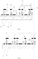
- the present invention provides a integrated structure of an MEMS pressure sensor and an MEMS inertia sensor, comprising: a substrate 1, an insulating layer 2 formed on the substrate 1, a first lower electrode 3a and a second lower electrode 3b both formed on the insulating layer 2, further comprising a first upper electrode 4a supported above the first lower electrode 3a by a first support part 7a, and a second upper electrode 4b supported above the second lower electrode 3b by a second support part 7b, wherein the first upper electrode 4a is a pressure-sensitive film and a cavity between the first upper electrode 4a and the first lower electrode 3a is an airtight cavity 9a, so that the first upper electrode 4a and the first lower electrode 4b form an air pressure-sensitive capacitor of the pressure sensor.
- the airtight cavity 9a is optionally a vacuum cavity.
- the second upper electrode 4b and the second lower electrode 3b form a reference capacitor whose capacitance is not changed along with the outside air pressure.
- the integrated structure according to the present invention further comprises an inertia-sensitive structure 4c supported above the substrate 1 by a third support part 7c, and a fixed electrode plate forming an inertia detecting capacitor together with the inertia-sensitive structure 4c.
- the inertia-sensitive structure 4c of the MEMS inertia sensor belongs to prior art for those skilled in the art, which has symmetric movable electrode plates and may be connected to the third support part 7c via an elastic beam structure.
- the fixed electrode plate is disposed on the insulating layer 2 and located below the inertia-sensitive structure 4c as a third lower electrode 3c of the inertia detecting capacitor, so that the MEMS inertia sensor may detect in Z axis.
- those skilled in the art may also dispose the fixed electrode plate opposed to the lateral surface of the inertia-sensitive structure 4c so that the fixed electrode plate and the inertia-sensitive structure 4c may form an inertia detecting capacitor that may detect in X axis and Y axis directions.
- the MEMS inertia sensor of the present invention may be inertia sensors such as an MEMS accelerometer, an MEMS gyroscope and an MEMS resonator.
- the insulating layer 2 plays a role in guaranteeing insulation between various parts and the substrate 1. To those skilled in the art, if the substrate 1 per se is made of insulating material, there is no need to set up the insulating layer 2.
- the integrated structure according to the present invention further comprises a cover body 8 which packages the inertia detecting capacitor composed of the inertia-sensitive structure 4c and the fixed electrode plate on the substrate 1, wherein the cover body 8 may be directly disposed on the insulating layer 2 above the substrate 1.
- a fourth support part 7d may be disposed on the insulating layer 2, and the cover body 8 and the fourth support part 7d are connected together to form the cavity packaging the inertia detecting capacitor.
- the cover body 8 of the present invention may package the reference capacitor composed of the second upper electrode 4b and the second lower electrode 3b on the substrate 1, as shown in Figs. 1 and 4 .
- the integrated structure according to the present invention integrates the MEMS inertia sensor and the MEMS pressure sensor on the same substrate, which may effectively reduce the area of the chip, so as to reduce the cost of the chip.
- a single packaging process may complete the packaging of the entire chip and reduce the cost of the chip packaging.
- substantially consistent responses to the outside common-mode interference signals may be generated.
- the common-mode interference signal in output signals of the air pressure-sensitive capacitor may be at least partially filtered using the output signal of the reference capacitor, and improving the stability of the output signals of the air pressure-sensitive capacitor.
- the second upper electrode 4b may apply a pressure-sensitive film.
- the first upper electrode 4a and the second upper electrode 4b may be mutually independent or may be integrated (i.e. the first upper electrode 4a and the second upper electrode 4b are a single pressure-sensitive film), as shown in Fig. 3 .
- the reference capacitor further includes a position-limiting structure for constraining the second upper electrode 4b from deforming under the outside air pressure.
- the second upper electrode 4b may be made of materials that do not deform within the detection range of the pressure sensor of the present invention, and the materials preferably cause the difference in the response of the second upper electrode 4b and the first upper electrode 4a to the change of non-air pressure factors such as temperature to be within the permitted error range of the pressure sensor.
- the position-limiting structure is as follows: a pressure balancing hole 12 is disposed for the reference capacitor so that the cavity 9b between the second upper electrode 4b and the second lower electrode 3b in the reference capacitor is communicated with the outside via the pressure balancing hole 12, in this way, the air pressure within the cavity 9b will change likewise according to the outside air pressure, achieving the purpose of constraining the second upper electrode 4b from deforming under application of the outside air pressure via the pressure balancing hole 12, and obtaining the effect of keeping the positions of the various points on the second upper electrode 4b unchanged.
- the pressure balancing hole 12 may be disposed on the second upper electrode 4b to simplify the manufacturing process of the pressure sensor.
- the pressure balancing hole 12 may be disposed on the second support part 7b, which may also achieve the same purpose of balancing air pressure.
- the above-mentioned position-limiting structure may be as follows: a supporting column 13 is disposed to support the second upper electrode 4b, the supporting column 13 may be disposed on the second lower electrode 3b.
- the support column 13 needs to be made of the insulating material, in order to improve the connecting intension of the supporting column 13, the supporting column 13 may also be disposed on the insulating layer 2, which requires to dispose a through hole on the second lower electrode 3b for the supporting column 13 to pass through, so that the supporting column 13 passes through the corresponding through hole and extends upwards until the position of the second upper electrode 4b.
- the first support part 7a, the second support part 7b, the third support part 7c and the fourth support part 7d are made of the same material, e.g., silica materials, and have the same height;
- the first upper electrode 4a, the second upper electrode 4b and the inertia-sensitive structure 4c are made of the same material, e.g., monocrystalline silicon materials, and have the same height;
- the first lower electrode 3a, the second lower electrode 3b and the third lower electrode 3c are made of the same material, e.g., metal materials, and have the same height.
- this allows the above various layers to be disposed via deposition layer by layer or bonding, and forms respective structures via graphical process.
- the manufacturing process of the MEMS inertia sensor is completely compatible with the process of the MEMS pressure sensor. More importantly, the same material, process and size may make the air pressure-sensitive capacitor and the reference capacitor have basically identical initial capacitance, so that the responses of the air pressure-sensitive capacitor and the reference capacitor to the outside common-mode interference are basically identical, so as to filter the common-mode interference signal in the output signals of the air pressure-sensitive capacitor to the maximum degree, and eliminate the influence of output signals of the reference capacitor to effective signals among the output signals of the air pressure-sensitive capacitor.
- the lower end faces of the first upper electrode 4a and the second upper electrode 4b are higher than the lower end faces of the inertia-sensitive structure 4c.
- it may be realized by etching and thinning the lower end faces of the first upper electrode 4a and the second upper electrode 4b, thereby increasing the volume of the airtight cavity 9a and the cavity 9b, ensuring the consistency of the air pressure-sensitive capacitor and the reference capacitor and improving sensitivity of the air pressure-sensitive type capacitor.
- thinning the lower end face of the first upper electrode 4a may increase the distance from the first upper electrode 4a to the first lower electrode 3a. While preventing high pressure input, the first upper electrode 4a and the first lower electrode 3a are adhered together to cause the air pressure-sensitive capacitor to lose effect.
- the first support part 7a, the second support part 7b, and the third support part 7c are respectively provided with through holes, conductive materials 6 electrically connected with the first upper electrode 4a, the second upper electrode 4b and the inertial sensitive structure 4c are respectively disposed in the through holes, so that the signals of the electrodes in the upper part are lead to the lower ends, and the lower ends of the first support part 7a, the second support part 7b, and the third support part 7c form a plurality of corresponding connecting leads 5, the plurality of corresponding connecting leads 5 pass the insulating layer 2 and are respectively connected to a bonding pad concentration area 10 on the substrate 1.
- the insulating layer 2 may be designed with a multi-layer structure to make the plurality of connecting leads 5 stagger from each other; such lead passing way belongs to common general knowledge of those skilled in the art and will not be described here
- the present invention further provides a manufacturing method of the above-mentioned integrated structure.
- the method comprises: first of all, depositing the insulating layer 2 on the substrate 1, wherein the substrate 1 may be made of monocrystalline silicon materials, the insulating layer 2 may be made of silica materials; secondly, depositing a metal layer on an upper surface of the insulating layer 2 and etching the metal layer, forming the bonding pad concentration area 10, the first lower electrode 3a, the second lower electrode 3b and the third lower electrode 3c; after that, depositing another insulating layer and etching to form the first support part 7a, the second support part 7b, the third support part 7c and the fourth support part 7d; bonding the sensitive film layer on the support parts by means of bonding, etching the sensitive film layer, forming the first upper electrode 4a, the second upper electrode 4b and the inertia-sensitive structure 4c.
- the method may comprise: firstly etching through holes on the first support part 7a, the second support part 7b and the third support part 7c, after bonding the sensitive film layer, etching the sensitive film layer in the through hole position, filling a conductive material 6 to lead electrical signals of the first upper electrode 4a, the second upper electrode 4b and the inertia-sensitive structure 4c to the lower ends, and passing the leads via the insulating layer; in subsequent process, depositing another metal layer on an upper surface of the sensitive film layer, and etching and forming a conductive bonding pad above the conductive material 6 and a metal bonding layer 11 above the fourth support part 7d, finally, bonding the cover body 8 on the fourth support part 7d via the metal binding layer 11.
- the sensitive film layer above the fourth support part 7d may be retained, and bonded with the cover body 8 via the subsequent metal bonding layer 11.
- the above-mentioned insulating layer 2 may be integrated or include a plurality of independent sub-insulating layers corresponding to the air pressure-sensitive capacitor, the reference capacitor and the inertia detecting capacitor respectively; the first support part 7a, the second support part 7b, the third support part 7c and the fourth support part 7d are made of insulating materials, and may be independent from one another or may be an integrated structure.
Landscapes
- Engineering & Computer Science (AREA)
- Microelectronics & Electronic Packaging (AREA)
- Manufacturing & Machinery (AREA)
- Computer Hardware Design (AREA)
- Physics & Mathematics (AREA)
- General Physics & Mathematics (AREA)
- Chemical & Material Sciences (AREA)
- Analytical Chemistry (AREA)
- Measuring Fluid Pressure (AREA)
- Pressure Sensors (AREA)
- Micromachines (AREA)
Applications Claiming Priority (2)
| Application Number | Priority Date | Filing Date | Title |
|---|---|---|---|
| CN201510288750.8A CN104891418B (zh) | 2015-05-29 | 2015-05-29 | Mems压力传感器、mems惯性传感器集成结构 |
| PCT/CN2015/097314 WO2016192372A1 (fr) | 2015-05-29 | 2015-12-14 | Structure d'intégration de capteur de pression mems et de capteur inertiel mems |
Publications (3)
| Publication Number | Publication Date |
|---|---|
| EP3248936A1 true EP3248936A1 (fr) | 2017-11-29 |
| EP3248936A4 EP3248936A4 (fr) | 2018-04-25 |
| EP3248936B1 EP3248936B1 (fr) | 2021-01-27 |
Family
ID=54024463
Family Applications (1)
| Application Number | Title | Priority Date | Filing Date |
|---|---|---|---|
| EP15894015.5A Active EP3248936B1 (fr) | 2015-05-29 | 2015-12-14 | Structure d'intégration de capteur de pression mems et de capteur inertiel mems |
Country Status (6)
| Country | Link |
|---|---|
| US (1) | US10407300B2 (fr) |
| EP (1) | EP3248936B1 (fr) |
| JP (2) | JP2018506717A (fr) |
| KR (1) | KR101975131B1 (fr) |
| CN (1) | CN104891418B (fr) |
| WO (1) | WO2016192372A1 (fr) |
Cited By (1)
| Publication number | Priority date | Publication date | Assignee | Title |
|---|---|---|---|---|
| WO2020127283A1 (fr) * | 2018-12-21 | 2020-06-25 | Robert Bosch Gmbh | Ensemble capteur micromécanique et procédé pour la fabrication d'un ensemble capteur micromécanique |
Families Citing this family (24)
| Publication number | Priority date | Publication date | Assignee | Title |
|---|---|---|---|---|
| CN104848982B (zh) | 2015-05-29 | 2018-01-19 | 歌尔股份有限公司 | 准差分电容式mems压力传感器及其制造方法 |
| CN104891418B (zh) | 2015-05-29 | 2016-09-21 | 歌尔股份有限公司 | Mems压力传感器、mems惯性传感器集成结构 |
| CN106698328A (zh) * | 2015-11-12 | 2017-05-24 | 上海丽恒光微电子科技有限公司 | 压力传感器及其制备方法 |
| US9926190B2 (en) * | 2016-01-21 | 2018-03-27 | Taiwan Semiconductor Manufacturing Company, Ltd. | MEMS devices and methods of forming the same |
| CN106018879B (zh) * | 2016-05-12 | 2019-03-22 | 广东合微集成电路技术有限公司 | 一种mems加速度传感器及制造方法 |
| CN106092153B (zh) * | 2016-07-28 | 2018-05-01 | 歌尔股份有限公司 | 一种环境传感器及其制造方法 |
| EP3279630B1 (fr) * | 2016-08-03 | 2019-06-26 | ams AG | Module de capteur de pression |
| CN107089640B (zh) * | 2017-05-02 | 2023-11-10 | 潍坊歌尔微电子有限公司 | 一种mems芯片及制备方法 |
| CN107830966B (zh) * | 2017-12-05 | 2023-08-29 | 苏州科技大学 | Mems气体压力敏感元件及其制造工艺 |
| CN108178121B (zh) * | 2018-02-07 | 2024-05-03 | 北京先通康桥医药科技有限公司 | 触诊探头及其制造方法 |
| CN108190828B (zh) * | 2018-02-07 | 2024-08-13 | 北京先通康桥医药科技有限公司 | Mems传感器线阵、触诊探头及其制造方法 |
| CN108362408B (zh) * | 2018-03-08 | 2021-07-02 | 苏州敏芯微电子技术股份有限公司 | 压力传感器及其制造方法 |
| CN108551646B (zh) * | 2018-06-25 | 2020-01-17 | 歌尔股份有限公司 | Mems麦克风 |
| CN109859986A (zh) * | 2019-01-31 | 2019-06-07 | 王伟 | 一种基于mems技术的单刀双掷敏感组件及含有该敏感组件的压力开关 |
| CN112666236A (zh) * | 2020-04-17 | 2021-04-16 | 华中科技大学 | 一种传感器集成芯片及其制备 |
| US11703521B2 (en) * | 2020-12-04 | 2023-07-18 | Honeywell International Inc. | MEMS vibrating beam accelerometer with built-in test actuators |
| CN113257808B (zh) * | 2021-05-17 | 2023-04-07 | 成都挚信电子技术有限责任公司 | 一种芯片衬底外延片 |
| IT202100022511A1 (it) | 2021-08-30 | 2023-03-02 | St Microelectronics Srl | Procedimento di fabbricazione di un sistema integrato includente un sensore di pressione capacitivo e un sensore inerziale, e sistema integrato |
| CN218491481U (zh) * | 2021-08-30 | 2023-02-17 | 意法半导体股份有限公司 | 半导体器件 |
| CN114235237A (zh) * | 2021-12-21 | 2022-03-25 | 苏州感芯微系统技术有限公司 | 一种平衡式结构体的硅压传感器芯片 |
| CN114858165B (zh) * | 2022-07-06 | 2022-11-29 | 河北美泰电子科技有限公司 | 惯性导航总成 |
| CN115452901B (zh) * | 2022-09-15 | 2024-11-12 | 武汉高芯科技有限公司 | 一种具有检测功能的传感器及检测方法 |
| CN119483529A (zh) * | 2023-08-09 | 2025-02-18 | 北京京东方传感技术有限公司 | 滤波器及其制备方法、电子设备 |
| CN118500483B (zh) * | 2024-07-17 | 2024-11-12 | 苏州敏芯微电子技术股份有限公司 | 传感器集成结构、芯片和制作方法 |
Family Cites Families (23)
| Publication number | Priority date | Publication date | Assignee | Title |
|---|---|---|---|---|
| US5369544A (en) * | 1993-04-05 | 1994-11-29 | Ford Motor Company | Silicon-on-insulator capacitive surface micromachined absolute pressure sensor |
| JP3432780B2 (ja) * | 2000-02-22 | 2003-08-04 | 株式会社日立製作所 | 半導体圧力センサ |
| JP2007064920A (ja) * | 2005-09-02 | 2007-03-15 | Alps Electric Co Ltd | 静電容量型力学量センサ |
| JP5127210B2 (ja) * | 2006-11-30 | 2013-01-23 | 株式会社日立製作所 | Memsセンサが混載された半導体装置 |
| US8220330B2 (en) * | 2009-03-24 | 2012-07-17 | Freescale Semiconductor, Inc. | Vertically integrated MEMS sensor device with multi-stimulus sensing |
| US8216882B2 (en) | 2010-08-23 | 2012-07-10 | Freescale Semiconductor, Inc. | Method of producing a microelectromechanical (MEMS) sensor device |
| CN102180435B (zh) * | 2011-03-15 | 2012-10-10 | 迈尔森电子(天津)有限公司 | 集成mems器件及其形成方法 |
| CN102183335B (zh) * | 2011-03-15 | 2015-10-21 | 迈尔森电子(天津)有限公司 | Mems压力传感器及其制作方法 |
| CN102183677B (zh) * | 2011-03-15 | 2012-08-08 | 迈尔森电子(天津)有限公司 | 集成惯性传感器与压力传感器及其形成方法 |
| JP5541306B2 (ja) * | 2011-05-27 | 2014-07-09 | 株式会社デンソー | 力学量センサ装置およびその製造方法 |
| KR101646999B1 (ko) * | 2011-06-29 | 2016-08-09 | 인벤센스, 인크. | 수직으로 집적된 전자장치를 갖는 환경에 노출된 부분을 구비한 기밀하게 밀봉된 mems 디바이스 |
| DE102011085723A1 (de) * | 2011-11-03 | 2013-05-08 | Continental Teves Ag & Co. Ohg | Bauelement und Verfahren zur Herstellung eines Bauelements |
| CN103517169B (zh) | 2012-06-22 | 2017-06-09 | 英飞凌科技股份有限公司 | 具有可调节通风开口的mems结构及mems装置 |
| CN102798403B (zh) | 2012-08-21 | 2014-10-22 | 江苏物联网研究发展中心 | Mems薄膜电容式多参数传感器的集成制造方法 |
| US20150102437A1 (en) * | 2013-10-14 | 2015-04-16 | Freescale Semiconductor, Inc. | Mems sensor device with multi-stimulus sensing and method of fabrication |
| CN103708409B (zh) * | 2013-10-25 | 2015-10-07 | 张家港丽恒光微电子科技有限公司 | 压力传感器和惯性传感器及其形成方法 |
| US9199840B2 (en) * | 2013-11-01 | 2015-12-01 | Freescale Semiconductor, Inc. | Sensor protective coating |
| CN103712720B (zh) * | 2014-01-02 | 2015-08-19 | 杭州士兰集成电路有限公司 | 电容式压力传感器和惯性传感器集成器件及其形成方法 |
| US20160264403A1 (en) * | 2015-03-12 | 2016-09-15 | Freescale Semiconducto, Inc. | Sensor device with multi-stimulus sensing and method of fabrication |
| US9586812B2 (en) * | 2015-04-09 | 2017-03-07 | Nxp Usa, Inc. | Device with vertically integrated sensors and method of fabrication |
| CN104891418B (zh) * | 2015-05-29 | 2016-09-21 | 歌尔股份有限公司 | Mems压力传感器、mems惯性传感器集成结构 |
| CN204675826U (zh) * | 2015-05-29 | 2015-09-30 | 歌尔声学股份有限公司 | Mems压力传感器、mems惯性传感器集成结构 |
| US10364140B2 (en) * | 2015-09-22 | 2019-07-30 | Nxp Usa, Inc. | Integrating diverse sensors in a single semiconductor device |
-
2015
- 2015-05-29 CN CN201510288750.8A patent/CN104891418B/zh active Active
- 2015-12-14 JP JP2017539547A patent/JP2018506717A/ja active Pending
- 2015-12-14 EP EP15894015.5A patent/EP3248936B1/fr active Active
- 2015-12-14 US US15/554,652 patent/US10407300B2/en active Active
- 2015-12-14 KR KR1020177019439A patent/KR101975131B1/ko active Active
- 2015-12-14 WO PCT/CN2015/097314 patent/WO2016192372A1/fr not_active Ceased
-
2019
- 2019-03-04 JP JP2019038245A patent/JP6580804B2/ja active Active
Cited By (3)
| Publication number | Priority date | Publication date | Assignee | Title |
|---|---|---|---|---|
| WO2020127283A1 (fr) * | 2018-12-21 | 2020-06-25 | Robert Bosch Gmbh | Ensemble capteur micromécanique et procédé pour la fabrication d'un ensemble capteur micromécanique |
| CN113227741A (zh) * | 2018-12-21 | 2021-08-06 | 罗伯特·博世有限公司 | 微机械传感器装置和用于制造微机械传感器装置的方法 |
| US11912565B2 (en) | 2018-12-21 | 2024-02-27 | Robert Bosch Gmbh | Micromechanical sensor unit and method for manufacturing a micromechanical sensor unit |
Also Published As
| Publication number | Publication date |
|---|---|
| EP3248936A4 (fr) | 2018-04-25 |
| JP2018506717A (ja) | 2018-03-08 |
| US10407300B2 (en) | 2019-09-10 |
| JP6580804B2 (ja) | 2019-09-25 |
| JP2019105647A (ja) | 2019-06-27 |
| CN104891418B (zh) | 2016-09-21 |
| WO2016192372A1 (fr) | 2016-12-08 |
| US20180044174A1 (en) | 2018-02-15 |
| EP3248936B1 (fr) | 2021-01-27 |
| CN104891418A (zh) | 2015-09-09 |
| KR20170094425A (ko) | 2017-08-17 |
| KR101975131B1 (ko) | 2019-05-03 |
Similar Documents
| Publication | Publication Date | Title |
|---|---|---|
| EP3248936B1 (fr) | Structure d'intégration de capteur de pression mems et de capteur inertiel mems | |
| US10551263B2 (en) | MEMS pressure sensing element | |
| US10295422B2 (en) | Quasi-differential capacitive MEMS pressure sensor and manufacturing methods thereof | |
| CN105181186B (zh) | 一种压力传感元件及其制造方法 | |
| CN106535071B (zh) | Mems麦克风与环境传感器的集成装置及其制造方法 | |
| US20160209344A1 (en) | Complex sensor and method of manufacturing the same | |
| CN204881958U (zh) | 准差分电容式mems压力传感器 | |
| CN110668394A (zh) | 一种抗干扰耐过载mems加速度计的制备方法 | |
| JP6258977B2 (ja) | センサおよびその製造方法 | |
| CN105115540B (zh) | Mems惯性传感器、湿度传感器集成装置及其制造方法 | |
| CN204675826U (zh) | Mems压力传感器、mems惯性传感器集成结构 | |
| US9963339B2 (en) | Sensor device | |
| CN106092153B (zh) | 一种环境传感器及其制造方法 | |
| US20160091526A1 (en) | Sensor | |
| JPH04249726A (ja) | 静電容量の変化を利用したセンサの製造方法 | |
| CN204758028U (zh) | Mems惯性传感器、湿度传感器集成装置 | |
| JP3938199B1 (ja) | ウェハレベルパッケージ構造体およびセンサ装置 | |
| CN108341394A (zh) | 微机电系统装置 | |
| US20200371130A1 (en) | Inertial sensor | |
| JP2008185374A (ja) | センサ装置の製造方法 | |
| JP2015021922A (ja) | 力学量センサ | |
| JP2010048785A (ja) | 電極基板及びこれを用いた静電容量型加速度センサ |
Legal Events
| Date | Code | Title | Description |
|---|---|---|---|
| STAA | Information on the status of an ep patent application or granted ep patent |
Free format text: STATUS: THE INTERNATIONAL PUBLICATION HAS BEEN MADE |
|
| PUAI | Public reference made under article 153(3) epc to a published international application that has entered the european phase |
Free format text: ORIGINAL CODE: 0009012 |
|
| STAA | Information on the status of an ep patent application or granted ep patent |
Free format text: STATUS: REQUEST FOR EXAMINATION WAS MADE |
|
| 17P | Request for examination filed |
Effective date: 20170823 |
|
| AK | Designated contracting states |
Kind code of ref document: A1 Designated state(s): AL AT BE BG CH CY CZ DE DK EE ES FI FR GB GR HR HU IE IS IT LI LT LU LV MC MK MT NL NO PL PT RO RS SE SI SK SM TR |
|
| AX | Request for extension of the european patent |
Extension state: BA ME |
|
| A4 | Supplementary search report drawn up and despatched |
Effective date: 20180326 |
|
| RIC1 | Information provided on ipc code assigned before grant |
Ipc: B81B 7/02 20060101AFI20180320BHEP Ipc: G01L 9/12 20060101ALI20180320BHEP |
|
| STAA | Information on the status of an ep patent application or granted ep patent |
Free format text: STATUS: EXAMINATION IS IN PROGRESS |
|
| 17Q | First examination report despatched |
Effective date: 20180705 |
|
| DAV | Request for validation of the european patent (deleted) | ||
| DAX | Request for extension of the european patent (deleted) | ||
| REG | Reference to a national code |
Ref country code: DE Ref legal event code: R079 Ref document number: 602015065365 Country of ref document: DE Free format text: PREVIOUS MAIN CLASS: B81C0001000000 Ipc: B81B0007020000 |
|
| RAP1 | Party data changed (applicant data changed or rights of an application transferred) |
Owner name: WEIFANG GOERTEK MICROELECTRONICS CO., LTD. |
|
| RIC1 | Information provided on ipc code assigned before grant |
Ipc: B81B 7/02 20060101AFI20200625BHEP |
|
| GRAP | Despatch of communication of intention to grant a patent |
Free format text: ORIGINAL CODE: EPIDOSNIGR1 |
|
| STAA | Information on the status of an ep patent application or granted ep patent |
Free format text: STATUS: GRANT OF PATENT IS INTENDED |
|
| INTG | Intention to grant announced |
Effective date: 20200817 |
|
| GRAS | Grant fee paid |
Free format text: ORIGINAL CODE: EPIDOSNIGR3 |
|
| GRAA | (expected) grant |
Free format text: ORIGINAL CODE: 0009210 |
|
| STAA | Information on the status of an ep patent application or granted ep patent |
Free format text: STATUS: THE PATENT HAS BEEN GRANTED |
|
| AK | Designated contracting states |
Kind code of ref document: B1 Designated state(s): AL AT BE BG CH CY CZ DE DK EE ES FI FR GB GR HR HU IE IS IT LI LT LU LV MC MK MT NL NO PL PT RO RS SE SI SK SM TR |
|
| REG | Reference to a national code |
Ref country code: GB Ref legal event code: FG4D |
|
| REG | Reference to a national code |
Ref country code: CH Ref legal event code: EP |
|
| REG | Reference to a national code |
Ref country code: AT Ref legal event code: REF Ref document number: 1358207 Country of ref document: AT Kind code of ref document: T Effective date: 20210215 |
|
| REG | Reference to a national code |
Ref country code: IE Ref legal event code: FG4D |
|
| REG | Reference to a national code |
Ref country code: DE Ref legal event code: R096 Ref document number: 602015065365 Country of ref document: DE |
|
| REG | Reference to a national code |
Ref country code: NL Ref legal event code: MP Effective date: 20210127 |
|
| REG | Reference to a national code |
Ref country code: LT Ref legal event code: MG9D |
|
| REG | Reference to a national code |
Ref country code: AT Ref legal event code: MK05 Ref document number: 1358207 Country of ref document: AT Kind code of ref document: T Effective date: 20210127 |
|
| PG25 | Lapsed in a contracting state [announced via postgrant information from national office to epo] |
Ref country code: HR Free format text: LAPSE BECAUSE OF FAILURE TO SUBMIT A TRANSLATION OF THE DESCRIPTION OR TO PAY THE FEE WITHIN THE PRESCRIBED TIME-LIMIT Effective date: 20210127 Ref country code: FI Free format text: LAPSE BECAUSE OF FAILURE TO SUBMIT A TRANSLATION OF THE DESCRIPTION OR TO PAY THE FEE WITHIN THE PRESCRIBED TIME-LIMIT Effective date: 20210127 Ref country code: GR Free format text: LAPSE BECAUSE OF FAILURE TO SUBMIT A TRANSLATION OF THE DESCRIPTION OR TO PAY THE FEE WITHIN THE PRESCRIBED TIME-LIMIT Effective date: 20210428 Ref country code: LT Free format text: LAPSE BECAUSE OF FAILURE TO SUBMIT A TRANSLATION OF THE DESCRIPTION OR TO PAY THE FEE WITHIN THE PRESCRIBED TIME-LIMIT Effective date: 20210127 Ref country code: BG Free format text: LAPSE BECAUSE OF FAILURE TO SUBMIT A TRANSLATION OF THE DESCRIPTION OR TO PAY THE FEE WITHIN THE PRESCRIBED TIME-LIMIT Effective date: 20210427 Ref country code: PT Free format text: LAPSE BECAUSE OF FAILURE TO SUBMIT A TRANSLATION OF THE DESCRIPTION OR TO PAY THE FEE WITHIN THE PRESCRIBED TIME-LIMIT Effective date: 20210527 Ref country code: NO Free format text: LAPSE BECAUSE OF FAILURE TO SUBMIT A TRANSLATION OF THE DESCRIPTION OR TO PAY THE FEE WITHIN THE PRESCRIBED TIME-LIMIT Effective date: 20210427 |
|
| PG25 | Lapsed in a contracting state [announced via postgrant information from national office to epo] |
Ref country code: SE Free format text: LAPSE BECAUSE OF FAILURE TO SUBMIT A TRANSLATION OF THE DESCRIPTION OR TO PAY THE FEE WITHIN THE PRESCRIBED TIME-LIMIT Effective date: 20210127 Ref country code: AT Free format text: LAPSE BECAUSE OF FAILURE TO SUBMIT A TRANSLATION OF THE DESCRIPTION OR TO PAY THE FEE WITHIN THE PRESCRIBED TIME-LIMIT Effective date: 20210127 Ref country code: PL Free format text: LAPSE BECAUSE OF FAILURE TO SUBMIT A TRANSLATION OF THE DESCRIPTION OR TO PAY THE FEE WITHIN THE PRESCRIBED TIME-LIMIT Effective date: 20210127 Ref country code: RS Free format text: LAPSE BECAUSE OF FAILURE TO SUBMIT A TRANSLATION OF THE DESCRIPTION OR TO PAY THE FEE WITHIN THE PRESCRIBED TIME-LIMIT Effective date: 20210127 Ref country code: LV Free format text: LAPSE BECAUSE OF FAILURE TO SUBMIT A TRANSLATION OF THE DESCRIPTION OR TO PAY THE FEE WITHIN THE PRESCRIBED TIME-LIMIT Effective date: 20210127 |
|
| PG25 | Lapsed in a contracting state [announced via postgrant information from national office to epo] |
Ref country code: IS Free format text: LAPSE BECAUSE OF FAILURE TO SUBMIT A TRANSLATION OF THE DESCRIPTION OR TO PAY THE FEE WITHIN THE PRESCRIBED TIME-LIMIT Effective date: 20210527 |
|
| REG | Reference to a national code |
Ref country code: DE Ref legal event code: R097 Ref document number: 602015065365 Country of ref document: DE |
|
| PG25 | Lapsed in a contracting state [announced via postgrant information from national office to epo] |
Ref country code: EE Free format text: LAPSE BECAUSE OF FAILURE TO SUBMIT A TRANSLATION OF THE DESCRIPTION OR TO PAY THE FEE WITHIN THE PRESCRIBED TIME-LIMIT Effective date: 20210127 Ref country code: CZ Free format text: LAPSE BECAUSE OF FAILURE TO SUBMIT A TRANSLATION OF THE DESCRIPTION OR TO PAY THE FEE WITHIN THE PRESCRIBED TIME-LIMIT Effective date: 20210127 Ref country code: SM Free format text: LAPSE BECAUSE OF FAILURE TO SUBMIT A TRANSLATION OF THE DESCRIPTION OR TO PAY THE FEE WITHIN THE PRESCRIBED TIME-LIMIT Effective date: 20210127 |
|
| PG25 | Lapsed in a contracting state [announced via postgrant information from national office to epo] |
Ref country code: SK Free format text: LAPSE BECAUSE OF FAILURE TO SUBMIT A TRANSLATION OF THE DESCRIPTION OR TO PAY THE FEE WITHIN THE PRESCRIBED TIME-LIMIT Effective date: 20210127 Ref country code: RO Free format text: LAPSE BECAUSE OF FAILURE TO SUBMIT A TRANSLATION OF THE DESCRIPTION OR TO PAY THE FEE WITHIN THE PRESCRIBED TIME-LIMIT Effective date: 20210127 Ref country code: DK Free format text: LAPSE BECAUSE OF FAILURE TO SUBMIT A TRANSLATION OF THE DESCRIPTION OR TO PAY THE FEE WITHIN THE PRESCRIBED TIME-LIMIT Effective date: 20210127 |
|
| PLBE | No opposition filed within time limit |
Free format text: ORIGINAL CODE: 0009261 |
|
| STAA | Information on the status of an ep patent application or granted ep patent |
Free format text: STATUS: NO OPPOSITION FILED WITHIN TIME LIMIT |
|
| 26N | No opposition filed |
Effective date: 20211028 |
|
| PG25 | Lapsed in a contracting state [announced via postgrant information from national office to epo] |
Ref country code: AL Free format text: LAPSE BECAUSE OF FAILURE TO SUBMIT A TRANSLATION OF THE DESCRIPTION OR TO PAY THE FEE WITHIN THE PRESCRIBED TIME-LIMIT Effective date: 20210127 Ref country code: ES Free format text: LAPSE BECAUSE OF FAILURE TO SUBMIT A TRANSLATION OF THE DESCRIPTION OR TO PAY THE FEE WITHIN THE PRESCRIBED TIME-LIMIT Effective date: 20210127 |
|
| PG25 | Lapsed in a contracting state [announced via postgrant information from national office to epo] |
Ref country code: SI Free format text: LAPSE BECAUSE OF FAILURE TO SUBMIT A TRANSLATION OF THE DESCRIPTION OR TO PAY THE FEE WITHIN THE PRESCRIBED TIME-LIMIT Effective date: 20210127 |
|
| PG25 | Lapsed in a contracting state [announced via postgrant information from national office to epo] |
Ref country code: IT Free format text: LAPSE BECAUSE OF FAILURE TO SUBMIT A TRANSLATION OF THE DESCRIPTION OR TO PAY THE FEE WITHIN THE PRESCRIBED TIME-LIMIT Effective date: 20210127 |
|
| PG25 | Lapsed in a contracting state [announced via postgrant information from national office to epo] |
Ref country code: IS Free format text: LAPSE BECAUSE OF FAILURE TO SUBMIT A TRANSLATION OF THE DESCRIPTION OR TO PAY THE FEE WITHIN THE PRESCRIBED TIME-LIMIT Effective date: 20210527 |
|
| PG25 | Lapsed in a contracting state [announced via postgrant information from national office to epo] |
Ref country code: MC Free format text: LAPSE BECAUSE OF FAILURE TO SUBMIT A TRANSLATION OF THE DESCRIPTION OR TO PAY THE FEE WITHIN THE PRESCRIBED TIME-LIMIT Effective date: 20210127 |
|
| REG | Reference to a national code |
Ref country code: CH Ref legal event code: PL |
|
| REG | Reference to a national code |
Ref country code: BE Ref legal event code: MM Effective date: 20211231 |
|
| PG25 | Lapsed in a contracting state [announced via postgrant information from national office to epo] |
Ref country code: LU Free format text: LAPSE BECAUSE OF NON-PAYMENT OF DUE FEES Effective date: 20211214 Ref country code: IE Free format text: LAPSE BECAUSE OF NON-PAYMENT OF DUE FEES Effective date: 20211214 |
|
| PG25 | Lapsed in a contracting state [announced via postgrant information from national office to epo] |
Ref country code: BE Free format text: LAPSE BECAUSE OF NON-PAYMENT OF DUE FEES Effective date: 20211231 |
|
| PG25 | Lapsed in a contracting state [announced via postgrant information from national office to epo] |
Ref country code: LI Free format text: LAPSE BECAUSE OF NON-PAYMENT OF DUE FEES Effective date: 20211231 Ref country code: CH Free format text: LAPSE BECAUSE OF NON-PAYMENT OF DUE FEES Effective date: 20211231 |
|
| PG25 | Lapsed in a contracting state [announced via postgrant information from national office to epo] |
Ref country code: HU Free format text: LAPSE BECAUSE OF FAILURE TO SUBMIT A TRANSLATION OF THE DESCRIPTION OR TO PAY THE FEE WITHIN THE PRESCRIBED TIME-LIMIT; INVALID AB INITIO Effective date: 20151214 |
|
| PG25 | Lapsed in a contracting state [announced via postgrant information from national office to epo] |
Ref country code: NL Free format text: LAPSE BECAUSE OF NON-PAYMENT OF DUE FEES Effective date: 20210127 Ref country code: CY Free format text: LAPSE BECAUSE OF FAILURE TO SUBMIT A TRANSLATION OF THE DESCRIPTION OR TO PAY THE FEE WITHIN THE PRESCRIBED TIME-LIMIT Effective date: 20210127 |
|
| PG25 | Lapsed in a contracting state [announced via postgrant information from national office to epo] |
Ref country code: MK Free format text: LAPSE BECAUSE OF FAILURE TO SUBMIT A TRANSLATION OF THE DESCRIPTION OR TO PAY THE FEE WITHIN THE PRESCRIBED TIME-LIMIT Effective date: 20210127 |
|
| PG25 | Lapsed in a contracting state [announced via postgrant information from national office to epo] |
Ref country code: TR Free format text: LAPSE BECAUSE OF FAILURE TO SUBMIT A TRANSLATION OF THE DESCRIPTION OR TO PAY THE FEE WITHIN THE PRESCRIBED TIME-LIMIT Effective date: 20210127 |
|
| PG25 | Lapsed in a contracting state [announced via postgrant information from national office to epo] |
Ref country code: MT Free format text: LAPSE BECAUSE OF FAILURE TO SUBMIT A TRANSLATION OF THE DESCRIPTION OR TO PAY THE FEE WITHIN THE PRESCRIBED TIME-LIMIT Effective date: 20210127 |
|
| PGFP | Annual fee paid to national office [announced via postgrant information from national office to epo] |
Ref country code: GB Payment date: 20251229 Year of fee payment: 11 |
|
| PGFP | Annual fee paid to national office [announced via postgrant information from national office to epo] |
Ref country code: FR Payment date: 20251230 Year of fee payment: 11 |
|
| PGFP | Annual fee paid to national office [announced via postgrant information from national office to epo] |
Ref country code: DE Payment date: 20251231 Year of fee payment: 11 |