EP3249687A1 - Anzeigetafel und herstellungsverfahren dafür sowie anzeigevorrichtung - Google Patents
Anzeigetafel und herstellungsverfahren dafür sowie anzeigevorrichtung Download PDFInfo
- Publication number
- EP3249687A1 EP3249687A1 EP15832873.2A EP15832873A EP3249687A1 EP 3249687 A1 EP3249687 A1 EP 3249687A1 EP 15832873 A EP15832873 A EP 15832873A EP 3249687 A1 EP3249687 A1 EP 3249687A1
- Authority
- EP
- European Patent Office
- Prior art keywords
- insulation layer
- ranges
- layer
- signal lines
- display panel
- Prior art date
- Legal status (The legal status is an assumption and is not a legal conclusion. Google has not performed a legal analysis and makes no representation as to the accuracy of the status listed.)
- Granted
Links
Images

Classifications
-
- H—ELECTRICITY
- H10—SEMICONDUCTOR DEVICES; ELECTRIC SOLID-STATE DEVICES NOT OTHERWISE PROVIDED FOR
- H10D—INORGANIC ELECTRIC SEMICONDUCTOR DEVICES
- H10D86/00—Integrated devices formed in or on insulating or conducting substrates, e.g. formed in silicon-on-insulator [SOI] substrates or on stainless steel or glass substrates
- H10D86/40—Integrated devices formed in or on insulating or conducting substrates, e.g. formed in silicon-on-insulator [SOI] substrates or on stainless steel or glass substrates characterised by multiple TFTs
- H10D86/60—Integrated devices formed in or on insulating or conducting substrates, e.g. formed in silicon-on-insulator [SOI] substrates or on stainless steel or glass substrates characterised by multiple TFTs wherein the TFTs are in active matrices
-
- H—ELECTRICITY
- H10—SEMICONDUCTOR DEVICES; ELECTRIC SOLID-STATE DEVICES NOT OTHERWISE PROVIDED FOR
- H10D—INORGANIC ELECTRIC SEMICONDUCTOR DEVICES
- H10D86/00—Integrated devices formed in or on insulating or conducting substrates, e.g. formed in silicon-on-insulator [SOI] substrates or on stainless steel or glass substrates
- H10D86/01—Manufacture or treatment
- H10D86/021—Manufacture or treatment of multiple TFTs
-
- H—ELECTRICITY
- H10—SEMICONDUCTOR DEVICES; ELECTRIC SOLID-STATE DEVICES NOT OTHERWISE PROVIDED FOR
- H10D—INORGANIC ELECTRIC SEMICONDUCTOR DEVICES
- H10D86/00—Integrated devices formed in or on insulating or conducting substrates, e.g. formed in silicon-on-insulator [SOI] substrates or on stainless steel or glass substrates
- H10D86/40—Integrated devices formed in or on insulating or conducting substrates, e.g. formed in silicon-on-insulator [SOI] substrates or on stainless steel or glass substrates characterised by multiple TFTs
- H10D86/441—Interconnections, e.g. scanning lines
-
- H—ELECTRICITY
- H10—SEMICONDUCTOR DEVICES; ELECTRIC SOLID-STATE DEVICES NOT OTHERWISE PROVIDED FOR
- H10K—ORGANIC ELECTRIC SOLID-STATE DEVICES
- H10K59/00—Integrated devices, or assemblies of multiple devices, comprising at least one organic light-emitting element covered by group H10K50/00
- H10K59/10—OLED displays
- H10K59/12—Active-matrix OLED [AMOLED] displays
- H10K59/124—Insulating layers formed between TFT elements and OLED elements
-
- H—ELECTRICITY
- H10—SEMICONDUCTOR DEVICES; ELECTRIC SOLID-STATE DEVICES NOT OTHERWISE PROVIDED FOR
- H10P—GENERIC PROCESSES OR APPARATUS FOR THE MANUFACTURE OR TREATMENT OF DEVICES COVERED BY CLASS H10
- H10P14/00—Formation of materials, e.g. in the shape of layers or pillars
- H10P14/60—Formation of materials, e.g. in the shape of layers or pillars of insulating materials
- H10P14/63—Formation of materials, e.g. in the shape of layers or pillars of insulating materials characterised by the formation processes
- H10P14/6326—Deposition processes
- H10P14/6328—Deposition from the gas or vapour phase
- H10P14/6334—Deposition from the gas or vapour phase using decomposition or reaction of gaseous or vapour phase compounds, i.e. chemical vapour deposition
-
- H—ELECTRICITY
- H10—SEMICONDUCTOR DEVICES; ELECTRIC SOLID-STATE DEVICES NOT OTHERWISE PROVIDED FOR
- H10W—GENERIC PACKAGES, INTERCONNECTIONS, CONNECTORS OR OTHER CONSTRUCTIONAL DETAILS OF DEVICES COVERED BY CLASS H10
- H10W20/00—Interconnections in chips, wafers or substrates
- H10W20/01—Manufacture or treatment
- H10W20/071—Manufacture or treatment of dielectric parts thereof
- H10W20/081—Manufacture or treatment of dielectric parts thereof by forming openings in the dielectric parts
- H10W20/082—Manufacture or treatment of dielectric parts thereof by forming openings in the dielectric parts the openings being tapered via holes
-
- H—ELECTRICITY
- H10—SEMICONDUCTOR DEVICES; ELECTRIC SOLID-STATE DEVICES NOT OTHERWISE PROVIDED FOR
- H10W—GENERIC PACKAGES, INTERCONNECTIONS, CONNECTORS OR OTHER CONSTRUCTIONAL DETAILS OF DEVICES COVERED BY CLASS H10
- H10W90/00—Package configurations
Definitions
- the present invention relates to the field of display technology, and particularly to a display panel and a method of fabricating the display panel, and a display device.
- a flat panel display device as a mainstream display device at present, is widely used in electronic products such as a computer screen, a mobile phone, etc., due to its characteristics of slim shape, power conservation, no radiation, etc.
- a display panel is a main component of the flat panel display device.
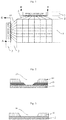
- the display panel comprises a pixel region 1, a fan-out region 2 and a driving circuit region 3.
- the pixel region 1 comprises a plurality of gate lines 11 and a plurality of data lines 12 provided to intersect each other, a first insulation layer 13 (generally, a gate insulation layer) is provided between the gate line 11 and the data line 12, a second insulation layer 14 (generally, a passivation layer) is provided on the data line 12, and the gate line 11 and the data line 12 extend into the fan-out region 2, respectively.
- the driving circuit region 3 comprises gate driving chips for supplying gate scanning signals to the gate lines 11, and source driving chips for supplying data voltage signals to the data lines 12. As shown in Figs.
- a first via hole 15 penetrating through the first insulation layer 13 and the second insulation layer 14 is formed on the gate line 11 in the fan-out region 2
- a second via hole 16 penetrating through the second insulation layer 14 is formed on the data line 12 in the fan-out region 2 so that the gate driving chip is electrically connected with the gate line 11 through the first via hole 15, and the source driving chip is electrically connected with the data line 12 through the second via hole 16.
- the first via hole 15 and the second via hole 16 are generally formed by one patterning process, thereby reducing processing steps and saving costs.
- the embodiments of the present invention provide a display panel and a method of fabricating the same, and a display device, which can effectively solve the problem that the pins of the driving chip cannot be wrapped completely due to relatively large size of the opening, thereby avoiding the failure caused by the exposure of the data lines below the pins.
- An embodiment of the present invention provides a display panel, comprising a pixel region and a fan-out region, a plurality of first signal lines and a plurality of second signal lines are provided to intersect each other in the pixel region, the first signal lines and the second signal lines extend into the fan-out region, respectively, a first insulation layer is provided between the first signal lines and the second signal lines, a second insulation layer is provided on the second signal lines, the second insulation layer comprises at least four layers of structures, and a density of each layer of structure of the second insulation layer decreases gradually along a direction away from the first insulation layer.
- Each layer of structure of the second insulation layer may be made of the same material.
- the display panel may further comprise a driving circuit region, the fan-out regions is provided between the pixel region and the driving circuit region, the driving circuit region comprises first driving chips and second driving chips, the first driving chip is electrically connected with the first signal lines through first via holes penetrating through the first insulation layer and the second insulation layer in the fan-out region, and the second driving chip is electrically connected with the second signal lines through second via holes penetrating through the second insulation layer in the fan-out region.
- the second via hole may have a step-like inner wall, and each step is positioned at an interface between any two adjacent layers of structures in the second insulation layer.
- a diameter of a circle formed by each step may sequentially increase along the direction away from the first insulation layer.
- the second insulation layer may comprise four layers of structures.
- Thicknesses of the four layers of structures of the second insulation layer may be sequentially in ranges of 10nm to 50nm, 50nm to 500nm, 50nm to 500nm and 10nm to 50nm along the direction away from the first insulation layer.
- Etch rates of the four layers of structures of the second insulation layer may be sequentially in ranges of 300nm/min to 600nm/min, 300nm/min to 800nm/min, 300nm/min to 1000nm/min and 300nm/min to 1500nm/min along the direction away from the first insulation layer.
- the etch rate of the second layer of structure may be smaller than that of the third layer of structure by 100nm/min to 700nm/min in the four layers of structures of the second insulation layer.
- the first signal line is a gate line
- the second signal line is a data line
- the first driving chip is a gate driving chip
- the second driving chip is a source driving chip.
- the first signal line is a data line
- the second signal line is a gate line
- the first driving chip is a source driving chip
- the second driving chip is a gate driving chip
- Another embodiment of the present invention provides a method of fabricating a display panel, the display panel comprises a pixel region and a fan-out region, the method comprises steps of sequentially forming first signal lines, a first insulation layer, second signal lines and a second insulation layer on a substrate, the first signal lines and the second signal lines are provided in the pixel region to intersect each other, and extend from the pixel region into the fan-out region, respectively, the step of forming the second insulation layer comprises sequentially forming, on the substrate having the second signal lines formed thereon, at least four layers of insulation films whose densities decrease gradually, to form the layers of structures of the second insulation layer.
- Each layer of structure of the second insulation layer may be made of the same material.
- the second insulation layer may comprise four layers of structures, the step of sequentially forming the four layers of structures of the second insulation layer on the substrate having the second signal lines formed thereon comprises: forming the second insulation layer by a chemical vapor deposition process using reaction gases of NH 3 , N 2 and SiH 4 under a temperature ranging from 250°C to 400°C.
- a flow rate of SiH 4 ranges from 500sccm to 1500sccm
- a flow rate of NH 3 ranges from 2000sccm to 4000sccm
- a flow rate of N 2 ranges from 10000sccm to 30000sccm
- a reaction power ranges from 3000W to 6000W
- a reaction pressure ranges from 500mtorr to 1000mtorr
- a reaction distance ranges from 500mils to 1500mils.
- the flow rate of SiH 4 ranges from 1000sccm to 2000sccm
- the flow rate of NH 3 ranges from 3000sccm to 5000sccm
- the flow rate of N 2 ranges from 10000sccm to 30000sccm
- the reaction power ranges from 3000W to 7000W
- the reaction pressure ranges from 800mtorr to 1500mtorr
- the reaction distance ranges from 800mils to 1500mils.
- the flow rate of SiH 4 ranges from 1000sccm to 2000sccm
- the flow rate of NH 3 ranges from 3000sccm to 7000sccm
- the flow rate of N 2 ranges from 10000sccm to 30000sccm
- the reaction power ranges from 3000W to 7000W
- the reaction pressure ranges from 1000mtorr to 2500mtorr
- the reaction distance ranges from 800mils to 1500mils.
- the flow rate of SiH 4 ranges from 1000sccm to 2000sccm
- the flow rate of NH 3 ranges from 4000sccm to 8000sccm
- the flow rate of N 2 ranges from 10000sccm to 30000sccm
- the reaction power ranges from 5000W to 7000W
- the reaction pressure ranges from 2000mtorr to 3000mtorr
- the reaction distance ranges from 800mils to 1500mils.
- the display panel may further comprise a driving circuit region, the fan-out region is provided between the pixel region and the driving circuit region, the driving circuit region comprises first driving chips and second driving chips, after forming the second insulation layer, the method may further comprise forming first via holes penetrating through the first insulation layer and the second insulation layer in the fan-out region, and forming second via holes penetrating through the second insulation layer in the fan-out region by patterning process, so that the first driving chip is electrically connected with the first signal lines through the first via holes, and the second driving chip is electrically connected with the second signal lines through the second via holes.
- the second via hole may have a step-like inner wall, and each step is positioned at an interface between any two adjacent layers of structures in the second insulation layer.
- a diameter of a circle formed by each step may increase sequentially along a direction away from the first insulation layer.
- Thicknesses of the four layers of structures of the second insulation layer may be sequentially in ranges of 10nm to 50nm, 50nm to 500nm, 50nm to 500nm and 10nm to 50nm along a direction away from the first insulation layer.
- Etch rates of the four layers of structures of the second insulation layer may be sequentially in ranges of 300nm/min to 600nm/min, 300nm/min to 800nm/min, 300nm/min to 1000nm/min and 300nm/min to 1500nm/min along a direction away from the first insulation layer.
- the etch rate of the second layer of structure may be smaller than that of the third layer of structure by 100nm/min to 700nm/min in the four layers of structures of the second insulation layer.
- Yet another embodiment of the present invention provides a display device, comprising the above described display panel.
- the via hole having a step-like inner wall is formed after etching the second insulation layer with such structure, and the aperture of the via hole is reduced accordingly, so as to avoid occurrence of exposure of the signal line.
- the above described display panel may be fabricated, the process of the method is simple and easy to implement.
- the display device of the embodiment of the present invention comprises the above described display panel, the yield of the display device is high and the display quality thereof is good.
- An embodiment of the present invention provides a display panel comprising a pixel region and a fan-out region, the pixel region comprises a plurality of first signal lines and a plurality of second signal lines provided to intersect each other, the first signal lines and the second signal lines extend into the fan-out region, respectively, a first insulation layer is provided between the first signal lines and the second signal lines, a second insulation layer is provided on the second signal lines, the second insulation layer comprises at least four layers of structures, and a density of each layer of structure decreases gradually along a direction away from the first insulation layer.
- the signal lines on the display panel are electrically connected with a driving chip, so as to supply signals to pixel units connected with the signal lines from the driving chip. These signal lines extend from the pixel region into the fan-out region.
- the driving chip is electrically connected with the signal lines.
- these signal lines are not provided in the same layer, and thus depths of the via holes are different either.
- these via holes are generally formed by one patterning process, and thus apertures of the via holes with relatively small depths are relatively large. Consequently, the pins of the driving chip cannot be completely wrapped by walls of the via holes after being inserted into the via holes, which results in exposure of a portion of the signal line below the via hole and further causes failure of the signal line, thereby affecting a display effect.
- the structure of the insulation layer (the second insulation layer) having shallow via holes formed therein is changed, i.e., the second insulation layer having at least four layers of structures is utilized, and the density of each layer of structure in the second insulation layer decreases gradually along the direction away from the first insulation layer (the gate insulation layer).
- the via hole having a step-like inner wall is formed, and the aperture of the via hole is reduced accordingly, so as to avoid occurrence of exposure of the signal line, and flexibly change a monitored size in production.
- a display panel comprises a pixel region, a fan-out region and a driving circuit region, each fan-out region is provided between the pixel region and the driving circuit region.
- First signal lines and second signal lines intersecting each other in different planes are provided in the pixel region, and the first signal lines and the second signal lines extend into the fan-out region, respectively.
- a first driving chip and a second driving chip are provided in the driving circuit region.
- a first insulation layer is provided between a layer where the first signal lines are provided and a layer where the second signal lines are provided, and a second insulation layer is provided on the second signal lines.
- the first driving chip is electrically connected with the first signal lines through first via holes penetrating through the first insulation layer and the second insulation layer on the first signal lines in the fan-out region
- the second driving chip is electrically connected with the second signal lines through second via holes penetrating through the second insulation layer on the second signal lines in the fan-out region.
- the second insulation layer in the embodiment comprises at least four layers of structures, and a density of each layer of structure of the second insulation layer decreases gradually along a direction away from the first insulation layer.
- the first signal lines may be gate lines 11, the second signal lines may be data lines 12, the first driving chip may be a gate driving chip, and the second driving chip may be a source driving chip.
- the first signal lines may be data lines 12, the second signal lines may be gate lines 11, the first driving chip may be a source driving chip, and the second driving chip may be a gate driving chip.
- the plurality of gate lines 11 and the plurality of data lines 12 intersecting each other define a plurality of pixel units
- a gate insulation layer 13 (the first insulation layer) is provided between the gate lines 11 and the data lines 12
- a passivation layer 14 (the second insulation layer) is provided on the data lines 12.
- the first via holes 15 are etched in the gate insulation layer 13 and the passivation layer 14 formed on the gate lines 11, close to the driving circuit region, in the fan-out region, to penetrate through the gate insulation layer 13 and the passivation layer 14, and the second via holes 16 are etched in the passivation layer 14 formed on the data lines 12 to penetrate through the passivation layer 14.
- the pins of the gate driving chip of the driving circuit region are electrically connected with the gate lines 11 through the first via holes 15, so as to supply gate scanning signals to the gate lines 11, and the pins of the source driving chip are electrically connected with the data lines 12 through the second via holes 16, so as to supply data voltage signals to the data lines 12.
- the passivation layer 14 comprises at least four layers of structures, i.e., the structures 14-1, 14-2, 14-3 and 14-4 shown in Fig. 4 , and the density of each layer of structure decreases gradually along the direction away from the gate insulation layer 13, so that the inner wall of the second via hole 16 formed by etching the passivation layer 14 has a circular step-like shape.
- the densities of two adjacent layers of structures are different, and thus etched degrees of the two layers of structures are also different, i.e., an aperture of the via hole formed in the layer of structure with a larger density is smaller than that of the via hole formed in the layer of structure with a smaller density, so that a step is easily formed at an interface between the adjacent layers of structures, and further, the aperture of the inner wall of the second via hole 16 gradually increases along the direction away from the gate insulation layer 13.
- a diameter of the pin that can be held by the second via hole 16 is actually the smallest aperture in the inner wall of the second via hole 16, i.e., the aperture of the via hole formed by etching the layer of structure with the largest density.
- the aperture of the second via hole 16 in the embodiment is smaller, thereby avoiding the exposure of the data line caused when the pins of the source driving chip cannot be completely wrapped by the second via hole 16 due to the large aperture of the second via hole 16, and further avoiding the display failure.
- the change in structure of the passivation layer 14 may also have a certain impact on the aperture of the first via hole 15.
- the density of the gate insulation layer 13 is larger than that of the layer of structure with the largest density in the passivation layer 14 (i.e., the first layer of structure 14-1 of the passivation layer 14), and thus the aperture of the first via hole 15 depends on the gate insulation layer 13.
- the aperture of the formed first via hole 15 may decrease to some extent due to the increasing difficulty in etching, but it will not prevent the pins of the gate driving chip from being inserted into the first via holes 15, and instead, the pins can be inserted into the first via holes 15 to be connected with the gate lines, as long as a small force is applied to press down the gate driving chip.
- each layer of structure of the passivation layer 14 is made of the same material.
- the process becomes simple and the productivity can be increased.
- layers of structures of the passivation layer 14 may be made of different materials, as long as the densities of the respective layers of structures of the passivation layer sequentially decrease along the direction away from the gate insulation layer 13, and the inner wall of the second via hole 16 formed after the passivation layer 14 is etched has a step-like shape.
- the material of the passivation layer 14 may be, but not limited to, silicon nitride, and may also be other insulation material such as silicon oxide, etc.
- the passivation layer 14 in the embodiment may be a passivation layer having four layers of structures. It is verified by experiments that, when the passivation layer 14 has two layers or three layers of structures having densities decreasing gradually, the via hole having the step-like inner wall cannot be formed, but a via hole having a convex arc-shaped inner wall is formed, after etching the passivation layer 14. It could be understood that, the via hole of this kind still cannot completely wrap the pins of the driving chip.
- the passivation layer 14 has five layers or more layers of structures, although the via hole having the step-like inner wall can be formed after etching the passivation layer 14, the process inevitably becomes complicated, the fabrication costs are increased and the efficiency is reduced, as the number of layers of structures of the passivation layer 14 increases.
- the passivation layer 14 having four layers of structures has a simple structure, and in this case, the via hole having the step-like inner wall may be formed after etching, the pins of the driving chip can be completely wrapped, and thus the problem of failure caused by the exposed data line existing in the prior art can be solved. Further, it is easy to fabricate of the passivation layer 14 with four layers of structures, and thus the fabrication time is saved and the productivity is increased.
- the thicknesses of the four layers of structures are in ranges of 10nm to 50nm, 50nm to 500nm, 50nm to 500nm and 10nm to 50nm, respectively.
- the embodiment is not limited thereto, and other ranges of the thicknesses may be set according to the specific situation.
- etch rates of the four layers of structures are in ranges of 300nm/min to 600nm/min, 300nm/min to 800nm/min, 300nm/min to 1000nm/min, and 300nm/min to 1500nm/min, respectively.
- the density of each layer of structure may be represented by the etch rate of the layer of structure in the passivation layer 14, the layer of structure having a relatively large density has a relatively low etch rate, and the layer of structure having a relatively small density has a relatively high etch rate.
- the density of each layer of structure of the passivation layer 14 may be set appropriately, so that the inner wall of the second via hole 16 formed by etching the passivation layer 14 are more likely to have annular steps. It is verified by experiments that, when the etch rate of the second layer of structure 14-2 of the passivation layer 14 is smaller than that of the third layer of structure 14-3 by 100nm/min to 700nm/min, that is, when the difference between the densities of the second layer of structure 14-2 and the third layer of structure 14-3 is relatively large, relatively perfect annular steps may be formed on the inner wall of the second via hole 16 formed by etching the passivation layer 14. In this case, the diameter of the annular (circular) step formed at the interface between the second layer of structure 14-2 and the third layer of structure 14-3 of the passivation layer 14 may be regarded as the aperture of the second via hole 16 to be monitored.
- the display panel comprises a pixel region, a fan-out region and a driving circuit region.
- the fan-out region is provided between the pixel region and the driving circuit region.
- the pixel region comprises a plurality of first signal lines and a plurality of second signal lines intersecting each other, and the first signal lines and the second signal lines extend into the fan-out region, respectively.
- a first insulation layer is provided between the first signal lines and the second signal lines, and a second insulation layer is provided on the second signal lines.
- the second insulation layer comprises at least four layers of structures, and a density of each layer of structure decreases gradually along a direction away from the first insulation layer.
- the driving circuit region comprises first driving chips and second driving chips.
- the first driving chips are electrically connected with the first signal lines through first via holes penetrating through the first insulation layer and the second insulation layer in the fan-out region
- the second driving chips are electrically connected with the second signal lines through second via holes penetrating through the second insulation layer in the fan-out region.
- the second insulation layer comprises four layers of structures, and the four layers of structures are made of the same material, which may be silicon nitride.
- the method of fabricating the display panel in the embodiment comprises the following steps 1 to 3.
- step 1 a pattern of the first signal lines and the first insulation layer are formed on a substrate.
- the substrate is made of transparent material such as glass and is subjected to a pre-cleaning process.
- a first metal film is formed on the substrate by sputtering, thermal evaporation, plasma enhanced chemical vapor deposition (PECVD), low pressure chemical vapor deposition (LPCVD), atmospheric pressure chemical vapor deposition (APCVD) or electron cyclotron resonance chemical vapor deposition (ECR-CVD), a pattern of the first signal lines is formed by performing a patterning process comprising exposure, development, etching and stripping on the first metal film, and then the first insulation layer is formed by plasma enhanced chemical vapor deposition, low pressure chemical vapor deposition, atmospheric pressure chemical vapor deposition or electron cyclotron resonance chemical vapor deposition or sputtering.
- PECVD plasma enhanced chemical vapor deposition
- LPCVD low pressure chemical vapor deposition
- APCVD atmospheric pressure chemical vapor deposition
- ECR-CVD electron cyclotron resonance chemical vapor deposition
- step 2 a pattern of the second signal lines and the second insulation layer are formed on the substrate subjected to the above step, by patterning process.
- the method of forming the second signal lines is the same as that of forming the first signal lines, and the detailed description thereof is omitted herein.
- the method of forming the second insulation layer is different from that of forming the first insulation layer.
- the step of forming the second insulation layer specifically comprises: sequentially forming the first layer to the fourth layer of the second insulation layer by a chemical vapor deposition process using reaction gases of NH 3 , N 2 and SiH 4 under a temperature ranging from 250°C to 400°C, and the specific processing conditions will be respectively described as follows.
- a flow rate of SiH 4 ranges from 500sccm to 1500sccm
- a flow rate of NH 3 ranges from 2000sccm to 4000sccm
- a flow rate of N 2 ranges from 10000sccm to 30000sccm
- a reaction power ranges from 3000W to 6000W
- a reaction pressure ranges from 500mtorr to 1000mtorr
- a reaction distance ranges from 500mils to 1500mils.
- the flow rate of SiH 4 ranges from 1000sccm to 2000sccm
- the flow rate of NH 3 ranges from 3000sccm to 5000sccm
- the flow rate of N 2 ranges from 10000sccm to 30000sccm
- the reaction power ranges from 3000W to 7000W
- the reaction pressure ranges from 800mtorr to 1500mtorr
- the reaction distance ranges from 800mils to 1500mils.
- the flow rate of SiH 4 ranges from 1000sccm to 2000sccm
- the flow rate of NH 3 ranges from 3000sccm to 7000sccm
- the flow rate of N 2 ranges from 10000sccm to 30000sccm
- the reaction power ranges from 3000W to 7000W
- the reaction pressure ranges from 1000mtorr to 2500mtorr
- the reaction distance ranges from 800mils to 1500mils.
- the flow rate of SiH 4 ranges from 1000sccm to 2000sccm
- the flow rate of NH 3 ranges from 4000sccm to 8000sccm
- the flow rate of N 2 ranges from 10000sccm to 30000sccm
- the reaction power ranges from 5000W to 7000W
- the reaction pressure ranges from 2000mtorr to 3000mtorr
- the reaction distance ranges from 800mils to 1500mils.
- the four layers of structures of the second insulation layer may be formed by adjusting the flow rates of the gases and controlling the reaction power, the reaction pressure and the reaction distance in practical applications.
- the flow rate of SiH 4 ranges from 1000sccm to 2000sccm
- the flow rate of NH 3 ranges from 2000sccm to 8000sccm
- the flow rate of N 2 ranges from 10000sccm to 30000sccm
- the reaction power ranges from 3000W to 7000W
- the reaction pressure ranges from 500mtorr to 3000mtorr
- the reaction distance ranges from 500mils to 1500mils.
- the flow rates of gases, the reaction power, the reaction pressure and the reaction distance differ in forming the respective layers of structures of the second insulation layer, so that the four layers of structures having different densities can be formed.
- How to control the flow rates of gases, the reaction power, the reaction pressure and the reaction distance so as to form films of the same material but having different densities are well known to a person skilled in the art, and the description thereof is omitted herein.
- the thicknesses of the four layers of structures are in ranges of 10nm to 50nm, 50nm to 500nm, 50nm to 500nm and 10nm to 50nm, respectively.
- the embodiment is not limited thereto, and other ranges of thicknesses may be set according to the specific situation.
- etch rates of the four layers of structures are in ranges of 300nm/min to 600nm/min, 300nm/min to 800nm/min, 300nm/min to 1000nm/min, and 300nm/min to 1500nm/min, respectively. It could be understood that, the density of each layer of structure may be represented by the etch rate of the layer of structure in the second insulation layer, the layer of structure having a relatively large density has a relatively low etch rate, and the layer of structure having a relatively small density has a relatively high etch rate.
- the density of each layer of structure of the second insulation layer may be set appropriately, so that annular steps are formed more easily in the inner wall of the second via hole in a subsequent step of etching the second insulation layer. It is verified by experiments that, when the etch rate of the second layer of structure of the second insulation layer is smaller than that of the third layer of structure by 100nm/min to 700nm/min, that is, when the difference between the densities of the second layer of structure and the third layer of structure is relatively large, relatively perfect annular steps may be formed on the inner wall of the second via hole in the subsequent step of etching the second insulation layer. In this case, the diameter of the annular step formed at the interface between the second layer of structure and the third layer of structure of the second insulation layer in the subsequent step may be regarded as the aperture of the second via hole to be monitored.
- step 3 a pattern comprising the first via holes and the second via holes are formed on the substrate subjected to the above steps, by patterning process.
- an organic film is formed on the fourth layer of structure of the second insulation layer by using a coating (comprising spin-coating) method.
- the organic film is made of organic resin, which comprises acrylic film-forming resin, phenolic film-forming resin, vinyl polymer film-forming resin or polyimide film-forming resin.
- the first via holes penetrating through the first insulation layer and the second insulation layer and used for connecting the first signal lines with the first driving chip and the second via holes penetrating through the second insulation layer and used for connecting the second signal lines with the second driving chip are formed by patterning process.
- the position of each step is the position of interface between any two adjacent layers of structures in the second insulation layer, and the diameter of the circle formed by each step increases sequentially along the direction away from the first insulation layer.
- the example of fabricating the second insulation layer having four layers of structures is only described in the embodiment, and a second insulation layer having more than four layers of structures may also be fabricated by the same method, as long as the flow rates of gases, the reaction power, the reaction pressure and the reaction distance are controlled correspondingly.
- the layers of structures of the formed second insulation layer comprise at least four layers, and thus the annular steps can be formed on the inner wall of the second via hole formed by etching the second insulation layer.
- the monitored aperture of the second via hole in the second insulation layer of the embodiment may be changed, that is, the monitored aperture of the second via hole may be reduced, so that the second insulation layer can completely wrap the pins of the second driving chip inserted into the second via holes, thereby preventing the external environment from contaminating the pins of the second driving chip and the second signal lines below the second via holes, and further avoiding the failure.
- Another embodiment of the present invention provides a display device comprising the display panel described in the above embodiment.
- the display device of the embodiment has a better performance and a higher yield.
- the display device of the embodiment may be a liquid crystal display device of any mode such as TN, ADS, IPS, LTPS, etc.
- the display device may be any product or component with a display function, such as a liquid crystal panel, a liquid crystal TV set, a display, a mobile phone, a navigator, etc.
Landscapes
- Engineering & Computer Science (AREA)
- Microelectronics & Electronic Packaging (AREA)
- Manufacturing & Machinery (AREA)
- Devices For Indicating Variable Information By Combining Individual Elements (AREA)
- Internal Circuitry In Semiconductor Integrated Circuit Devices (AREA)
- Chemical & Material Sciences (AREA)
- Chemical Kinetics & Catalysis (AREA)
Applications Claiming Priority (2)
| Application Number | Priority Date | Filing Date | Title |
|---|---|---|---|
| CN201510018279.0A CN104538407B (zh) | 2015-01-14 | 2015-01-14 | 显示面板及其制备方法、显示装置 |
| PCT/CN2015/087334 WO2016112684A1 (zh) | 2015-01-14 | 2015-08-18 | 显示面板及其制备方法、显示装置 |
Publications (3)
| Publication Number | Publication Date |
|---|---|
| EP3249687A1 true EP3249687A1 (de) | 2017-11-29 |
| EP3249687A4 EP3249687A4 (de) | 2018-10-24 |
| EP3249687B1 EP3249687B1 (de) | 2020-05-06 |
Family
ID=52853910
Family Applications (1)
| Application Number | Title | Priority Date | Filing Date |
|---|---|---|---|
| EP15832873.2A Active EP3249687B1 (de) | 2015-01-14 | 2015-08-18 | Herstelllungsverfahren einer anzeigetafel |
Country Status (4)
| Country | Link |
|---|---|
| US (1) | US9825063B2 (de) |
| EP (1) | EP3249687B1 (de) |
| CN (1) | CN104538407B (de) |
| WO (1) | WO2016112684A1 (de) |
Families Citing this family (12)
| Publication number | Priority date | Publication date | Assignee | Title |
|---|---|---|---|---|
| CN104538407B (zh) | 2015-01-14 | 2017-11-10 | 京东方科技集团股份有限公司 | 显示面板及其制备方法、显示装置 |
| CN105097839B (zh) * | 2015-07-20 | 2019-08-09 | 京东方科技集团股份有限公司 | 一种绝缘层、阵列基板及其制作方法、显示装置 |
| CN107331694B (zh) | 2017-09-04 | 2020-03-17 | 京东方科技集团股份有限公司 | 一种oled显示面板及其制备方法、oled显示装置 |
| CN111244039B (zh) | 2018-11-29 | 2025-03-07 | 合肥鑫晟光电科技有限公司 | 密封结构及其制作方法和显示装置 |
| CN109671669A (zh) * | 2018-12-25 | 2019-04-23 | 信利半导体有限公司 | 过孔加工方法、基板结构及显示装置 |
| CN113272881B (zh) * | 2019-11-15 | 2023-08-29 | 京东方科技集团股份有限公司 | 显示面板、拼接显示面板、其制备方法 |
| CN111323949A (zh) * | 2020-04-15 | 2020-06-23 | 昆山国显光电有限公司 | 阵列基板及显示面板 |
| EP4162345A1 (de) * | 2020-06-03 | 2023-04-12 | Apple Inc. | Biofeedback auf augenblickbasis |
| US12099654B1 (en) | 2021-06-21 | 2024-09-24 | Apple Inc. | Adaptation of electronic content |
| CN113782579B (zh) * | 2021-09-15 | 2025-03-28 | 京东方科技集团股份有限公司 | 显示基板及显示装置 |
| CN114678327A (zh) * | 2022-03-04 | 2022-06-28 | 惠科股份有限公司 | 阵列基板的制作方法、显示面板及显示装置 |
| CN115332273B (zh) * | 2022-10-14 | 2023-04-07 | 广州华星光电半导体显示技术有限公司 | 阵列基板、阵列基板的制作方法及显示面板 |
Family Cites Families (15)
| Publication number | Priority date | Publication date | Assignee | Title |
|---|---|---|---|---|
| JPH04142740A (ja) * | 1990-10-03 | 1992-05-15 | Oki Electric Ind Co Ltd | コンタクトホールの形成方法 |
| US6458657B1 (en) * | 2000-09-25 | 2002-10-01 | Macronix International Co., Ltd. | Method of fabricating gate |
| JP5234301B2 (ja) | 2005-10-03 | 2013-07-10 | Nltテクノロジー株式会社 | 薄膜トランジスタ、薄膜トランジスタアレイ基板、液晶表示装置およびそれらの製造方法 |
| US20080017859A1 (en) * | 2006-07-18 | 2008-01-24 | Tpo Displays Corp. | System for displaying images including thin film transistor device and method for fabricating the same |
| KR20100041165A (ko) * | 2008-10-13 | 2010-04-22 | 삼성전자주식회사 | 표시 장치 및 그를 포함하는 멀티 표시 장치 |
| JP2012038965A (ja) * | 2010-08-09 | 2012-02-23 | Lapis Semiconductor Co Ltd | 半導体装置及びその製造方法 |
| US8970799B2 (en) * | 2011-07-19 | 2015-03-03 | Panasonic Intellectual Property Management Co., Ltd. | Liquid crystal display device and method of manufacturing the same |
| CN202189209U (zh) | 2011-09-05 | 2012-04-11 | 京东方科技集团股份有限公司 | 引线结构、液晶显示屏引线区结构和液晶显示屏 |
| KR101945866B1 (ko) * | 2012-03-19 | 2019-02-11 | 삼성디스플레이 주식회사 | 차폐 도전체를 가지는 액정 표시 장치 |
| JP5838119B2 (ja) * | 2012-04-24 | 2015-12-24 | 株式会社ジャパンディスプレイ | 薄膜トランジスタ及びそれを用いた表示装置 |
| CN103117249A (zh) * | 2013-01-29 | 2013-05-22 | 信利半导体有限公司 | 像素电极上钝化层的制作方法、液晶显示器及其制作方法 |
| US9893088B2 (en) * | 2013-05-29 | 2018-02-13 | Joled Inc. | Thin film transistor device, method for manufacturing same and display device |
| US9117879B2 (en) * | 2013-12-30 | 2015-08-25 | Taiwan Semiconductor Manufacturing Company Ltd. | Semiconductor device and manufacturing method thereof |
| CN104538407B (zh) | 2015-01-14 | 2017-11-10 | 京东方科技集团股份有限公司 | 显示面板及其制备方法、显示装置 |
| CN204375751U (zh) * | 2015-01-14 | 2015-06-03 | 京东方科技集团股份有限公司 | 显示面板及显示装置 |
-
2015
- 2015-01-14 CN CN201510018279.0A patent/CN104538407B/zh not_active Expired - Fee Related
- 2015-08-18 EP EP15832873.2A patent/EP3249687B1/de active Active
- 2015-08-18 US US14/905,380 patent/US9825063B2/en not_active Expired - Fee Related
- 2015-08-18 WO PCT/CN2015/087334 patent/WO2016112684A1/zh not_active Ceased
Also Published As
| Publication number | Publication date |
|---|---|
| WO2016112684A1 (zh) | 2016-07-21 |
| US9825063B2 (en) | 2017-11-21 |
| US20160372489A1 (en) | 2016-12-22 |
| CN104538407A (zh) | 2015-04-22 |
| EP3249687B1 (de) | 2020-05-06 |
| EP3249687A4 (de) | 2018-10-24 |
| CN104538407B (zh) | 2017-11-10 |
Similar Documents
| Publication | Publication Date | Title |
|---|---|---|
| EP3249687A1 (de) | Anzeigetafel und herstellungsverfahren dafür sowie anzeigevorrichtung | |
| CN110246879B (zh) | 一种有机发光显示面板及装置 | |
| US9508867B2 (en) | Thin film transistor, array substrate, method of fabricating same, and display device | |
| CN105116655B (zh) | 液晶显示面板、阵列基板及其制造方法 | |
| US9268169B2 (en) | Display panel with pixel define layer, manufacturing method of pixel define layer of display panel, and display device | |
| CN102790012A (zh) | 阵列基板的制造方法及阵列基板、显示装置 | |
| US11450839B2 (en) | Display device and manufacturing method thereof comprising patterning light-emitting layer in opening region | |
| US11659729B2 (en) | Electronic device substrate, manufacturing method and display device | |
| US9716117B2 (en) | Method for producing a via, a method for producing an array substrate, an array substrate, and a display device | |
| KR20180116118A (ko) | 플렉시블 디스플레이 패널, 이를 갖는 플렉시블 디스플레이 장치, 및 그 제조 방법 | |
| US20170205655A1 (en) | Display substrate, manufacturing method thereof and display device | |
| US20170110587A1 (en) | Array substrate and manufacturing method thereof, display panel, display device | |
| CN103531593B (zh) | 像素结构、阵列基板、显示装置及像素结构的制造方法 | |
| JP2016520205A (ja) | アレイ基板およびその製作方法、当該アレイ基板を備える表示装置 | |
| US9299727B2 (en) | Array substrate and manufacturing method thereof as well as display panel | |
| US20170040251A1 (en) | Display substrate, manufacturing method thereof and display device | |
| US20150372012A1 (en) | Array substrate, method of producing array substrate, and display panel | |
| CN110323350A (zh) | 一种薄膜封装方法、薄膜封装结构、显示装置 | |
| CN204375751U (zh) | 显示面板及显示装置 | |
| US10312461B2 (en) | Flexible OLED display panel having a substrate with a titanium layer and method for manufacturing same | |
| CN102956551B (zh) | 阵列基板的制作方法、阵列基板及显示装置 | |
| TW201618168A (zh) | 顯示面板之製備方法 | |
| WO2020258465A1 (zh) | 一种阵列基板及其制作方法、显示面板 | |
| US20240036423A1 (en) | Array substrate and manufacturing method thereof | |
| CN104835827B (zh) | 显示面板 |
Legal Events
| Date | Code | Title | Description |
|---|---|---|---|
| STAA | Information on the status of an ep patent application or granted ep patent |
Free format text: STATUS: THE INTERNATIONAL PUBLICATION HAS BEEN MADE |
|
| PUAI | Public reference made under article 153(3) epc to a published international application that has entered the european phase |
Free format text: ORIGINAL CODE: 0009012 |
|
| STAA | Information on the status of an ep patent application or granted ep patent |
Free format text: STATUS: REQUEST FOR EXAMINATION WAS MADE |
|
| 17P | Request for examination filed |
Effective date: 20160224 |
|
| AK | Designated contracting states |
Kind code of ref document: A1 Designated state(s): AL AT BE BG CH CY CZ DE DK EE ES FI FR GB GR HR HU IE IS IT LI LT LU LV MC MK MT NL NO PL PT RO RS SE SI SK SM TR |
|
| AX | Request for extension of the european patent |
Extension state: BA ME |
|
| DAV | Request for validation of the european patent (deleted) | ||
| DAX | Request for extension of the european patent (deleted) | ||
| A4 | Supplementary search report drawn up and despatched |
Effective date: 20180926 |
|
| RIC1 | Information provided on ipc code assigned before grant |
Ipc: H01L 27/12 20060101AFI20180920BHEP Ipc: H01L 21/768 20060101ALI20180920BHEP Ipc: H01L 27/32 20060101ALI20180920BHEP Ipc: H01L 21/77 20170101ALI20180920BHEP |
|
| GRAP | Despatch of communication of intention to grant a patent |
Free format text: ORIGINAL CODE: EPIDOSNIGR1 |
|
| STAA | Information on the status of an ep patent application or granted ep patent |
Free format text: STATUS: GRANT OF PATENT IS INTENDED |
|
| INTG | Intention to grant announced |
Effective date: 20191129 |
|
| GRAS | Grant fee paid |
Free format text: ORIGINAL CODE: EPIDOSNIGR3 |
|
| GRAA | (expected) grant |
Free format text: ORIGINAL CODE: 0009210 |
|
| STAA | Information on the status of an ep patent application or granted ep patent |
Free format text: STATUS: THE PATENT HAS BEEN GRANTED |
|
| AK | Designated contracting states |
Kind code of ref document: B1 Designated state(s): AL AT BE BG CH CY CZ DE DK EE ES FI FR GB GR HR HU IE IS IT LI LT LU LV MC MK MT NL NO PL PT RO RS SE SI SK SM TR |
|
| REG | Reference to a national code |
Ref country code: GB Ref legal event code: FG4D |
|
| REG | Reference to a national code |
Ref country code: CH Ref legal event code: EP Ref country code: AT Ref legal event code: REF Ref document number: 1268199 Country of ref document: AT Kind code of ref document: T Effective date: 20200515 |
|
| REG | Reference to a national code |
Ref country code: IE Ref legal event code: FG4D |
|
| REG | Reference to a national code |
Ref country code: DE Ref legal event code: R096 Ref document number: 602015052459 Country of ref document: DE |
|
| REG | Reference to a national code |
Ref country code: LT Ref legal event code: MG4D |
|
| REG | Reference to a national code |
Ref country code: NL Ref legal event code: MP Effective date: 20200506 |
|
| PG25 | Lapsed in a contracting state [announced via postgrant information from national office to epo] |
Ref country code: GR Free format text: LAPSE BECAUSE OF FAILURE TO SUBMIT A TRANSLATION OF THE DESCRIPTION OR TO PAY THE FEE WITHIN THE PRESCRIBED TIME-LIMIT Effective date: 20200807 Ref country code: NO Free format text: LAPSE BECAUSE OF FAILURE TO SUBMIT A TRANSLATION OF THE DESCRIPTION OR TO PAY THE FEE WITHIN THE PRESCRIBED TIME-LIMIT Effective date: 20200806 Ref country code: LT Free format text: LAPSE BECAUSE OF FAILURE TO SUBMIT A TRANSLATION OF THE DESCRIPTION OR TO PAY THE FEE WITHIN THE PRESCRIBED TIME-LIMIT Effective date: 20200506 Ref country code: FI Free format text: LAPSE BECAUSE OF FAILURE TO SUBMIT A TRANSLATION OF THE DESCRIPTION OR TO PAY THE FEE WITHIN THE PRESCRIBED TIME-LIMIT Effective date: 20200506 Ref country code: PT Free format text: LAPSE BECAUSE OF FAILURE TO SUBMIT A TRANSLATION OF THE DESCRIPTION OR TO PAY THE FEE WITHIN THE PRESCRIBED TIME-LIMIT Effective date: 20200907 Ref country code: IS Free format text: LAPSE BECAUSE OF FAILURE TO SUBMIT A TRANSLATION OF THE DESCRIPTION OR TO PAY THE FEE WITHIN THE PRESCRIBED TIME-LIMIT Effective date: 20200906 Ref country code: SE Free format text: LAPSE BECAUSE OF FAILURE TO SUBMIT A TRANSLATION OF THE DESCRIPTION OR TO PAY THE FEE WITHIN THE PRESCRIBED TIME-LIMIT Effective date: 20200506 |
|
| PGFP | Annual fee paid to national office [announced via postgrant information from national office to epo] |
Ref country code: DE Payment date: 20200819 Year of fee payment: 6 |
|
| PG25 | Lapsed in a contracting state [announced via postgrant information from national office to epo] |
Ref country code: RS Free format text: LAPSE BECAUSE OF FAILURE TO SUBMIT A TRANSLATION OF THE DESCRIPTION OR TO PAY THE FEE WITHIN THE PRESCRIBED TIME-LIMIT Effective date: 20200506 Ref country code: BG Free format text: LAPSE BECAUSE OF FAILURE TO SUBMIT A TRANSLATION OF THE DESCRIPTION OR TO PAY THE FEE WITHIN THE PRESCRIBED TIME-LIMIT Effective date: 20200806 Ref country code: LV Free format text: LAPSE BECAUSE OF FAILURE TO SUBMIT A TRANSLATION OF THE DESCRIPTION OR TO PAY THE FEE WITHIN THE PRESCRIBED TIME-LIMIT Effective date: 20200506 Ref country code: HR Free format text: LAPSE BECAUSE OF FAILURE TO SUBMIT A TRANSLATION OF THE DESCRIPTION OR TO PAY THE FEE WITHIN THE PRESCRIBED TIME-LIMIT Effective date: 20200506 |
|
| REG | Reference to a national code |
Ref country code: AT Ref legal event code: MK05 Ref document number: 1268199 Country of ref document: AT Kind code of ref document: T Effective date: 20200506 |
|
| PG25 | Lapsed in a contracting state [announced via postgrant information from national office to epo] |
Ref country code: AL Free format text: LAPSE BECAUSE OF FAILURE TO SUBMIT A TRANSLATION OF THE DESCRIPTION OR TO PAY THE FEE WITHIN THE PRESCRIBED TIME-LIMIT Effective date: 20200506 Ref country code: NL Free format text: LAPSE BECAUSE OF FAILURE TO SUBMIT A TRANSLATION OF THE DESCRIPTION OR TO PAY THE FEE WITHIN THE PRESCRIBED TIME-LIMIT Effective date: 20200506 |
|
| PG25 | Lapsed in a contracting state [announced via postgrant information from national office to epo] |
Ref country code: ES Free format text: LAPSE BECAUSE OF FAILURE TO SUBMIT A TRANSLATION OF THE DESCRIPTION OR TO PAY THE FEE WITHIN THE PRESCRIBED TIME-LIMIT Effective date: 20200506 Ref country code: CZ Free format text: LAPSE BECAUSE OF FAILURE TO SUBMIT A TRANSLATION OF THE DESCRIPTION OR TO PAY THE FEE WITHIN THE PRESCRIBED TIME-LIMIT Effective date: 20200506 Ref country code: AT Free format text: LAPSE BECAUSE OF FAILURE TO SUBMIT A TRANSLATION OF THE DESCRIPTION OR TO PAY THE FEE WITHIN THE PRESCRIBED TIME-LIMIT Effective date: 20200506 Ref country code: DK Free format text: LAPSE BECAUSE OF FAILURE TO SUBMIT A TRANSLATION OF THE DESCRIPTION OR TO PAY THE FEE WITHIN THE PRESCRIBED TIME-LIMIT Effective date: 20200506 Ref country code: RO Free format text: LAPSE BECAUSE OF FAILURE TO SUBMIT A TRANSLATION OF THE DESCRIPTION OR TO PAY THE FEE WITHIN THE PRESCRIBED TIME-LIMIT Effective date: 20200506 Ref country code: IT Free format text: LAPSE BECAUSE OF FAILURE TO SUBMIT A TRANSLATION OF THE DESCRIPTION OR TO PAY THE FEE WITHIN THE PRESCRIBED TIME-LIMIT Effective date: 20200506 Ref country code: EE Free format text: LAPSE BECAUSE OF FAILURE TO SUBMIT A TRANSLATION OF THE DESCRIPTION OR TO PAY THE FEE WITHIN THE PRESCRIBED TIME-LIMIT Effective date: 20200506 Ref country code: SM Free format text: LAPSE BECAUSE OF FAILURE TO SUBMIT A TRANSLATION OF THE DESCRIPTION OR TO PAY THE FEE WITHIN THE PRESCRIBED TIME-LIMIT Effective date: 20200506 |
|
| REG | Reference to a national code |
Ref country code: DE Ref legal event code: R097 Ref document number: 602015052459 Country of ref document: DE |
|
| PG25 | Lapsed in a contracting state [announced via postgrant information from national office to epo] |
Ref country code: SK Free format text: LAPSE BECAUSE OF FAILURE TO SUBMIT A TRANSLATION OF THE DESCRIPTION OR TO PAY THE FEE WITHIN THE PRESCRIBED TIME-LIMIT Effective date: 20200506 Ref country code: PL Free format text: LAPSE BECAUSE OF FAILURE TO SUBMIT A TRANSLATION OF THE DESCRIPTION OR TO PAY THE FEE WITHIN THE PRESCRIBED TIME-LIMIT Effective date: 20200506 |
|
| PLBE | No opposition filed within time limit |
Free format text: ORIGINAL CODE: 0009261 |
|
| STAA | Information on the status of an ep patent application or granted ep patent |
Free format text: STATUS: NO OPPOSITION FILED WITHIN TIME LIMIT |
|
| PG25 | Lapsed in a contracting state [announced via postgrant information from national office to epo] |
Ref country code: MC Free format text: LAPSE BECAUSE OF FAILURE TO SUBMIT A TRANSLATION OF THE DESCRIPTION OR TO PAY THE FEE WITHIN THE PRESCRIBED TIME-LIMIT Effective date: 20200506 |
|
| REG | Reference to a national code |
Ref country code: CH Ref legal event code: PL |
|
| 26N | No opposition filed |
Effective date: 20210209 |
|
| GBPC | Gb: european patent ceased through non-payment of renewal fee |
Effective date: 20200818 |
|
| PG25 | Lapsed in a contracting state [announced via postgrant information from national office to epo] |
Ref country code: LI Free format text: LAPSE BECAUSE OF NON-PAYMENT OF DUE FEES Effective date: 20200831 Ref country code: LU Free format text: LAPSE BECAUSE OF NON-PAYMENT OF DUE FEES Effective date: 20200818 Ref country code: CH Free format text: LAPSE BECAUSE OF NON-PAYMENT OF DUE FEES Effective date: 20200831 |
|
| REG | Reference to a national code |
Ref country code: BE Ref legal event code: MM Effective date: 20200831 |
|
| PG25 | Lapsed in a contracting state [announced via postgrant information from national office to epo] |
Ref country code: SI Free format text: LAPSE BECAUSE OF FAILURE TO SUBMIT A TRANSLATION OF THE DESCRIPTION OR TO PAY THE FEE WITHIN THE PRESCRIBED TIME-LIMIT Effective date: 20200506 |
|
| PG25 | Lapsed in a contracting state [announced via postgrant information from national office to epo] |
Ref country code: FR Free format text: LAPSE BECAUSE OF NON-PAYMENT OF DUE FEES Effective date: 20200831 |
|
| PG25 | Lapsed in a contracting state [announced via postgrant information from national office to epo] |
Ref country code: GB Free format text: LAPSE BECAUSE OF NON-PAYMENT OF DUE FEES Effective date: 20200818 Ref country code: IE Free format text: LAPSE BECAUSE OF NON-PAYMENT OF DUE FEES Effective date: 20200818 Ref country code: BE Free format text: LAPSE BECAUSE OF NON-PAYMENT OF DUE FEES Effective date: 20200831 |
|
| REG | Reference to a national code |
Ref country code: DE Ref legal event code: R119 Ref document number: 602015052459 Country of ref document: DE |
|
| PG25 | Lapsed in a contracting state [announced via postgrant information from national office to epo] |
Ref country code: TR Free format text: LAPSE BECAUSE OF FAILURE TO SUBMIT A TRANSLATION OF THE DESCRIPTION OR TO PAY THE FEE WITHIN THE PRESCRIBED TIME-LIMIT Effective date: 20200506 Ref country code: MT Free format text: LAPSE BECAUSE OF FAILURE TO SUBMIT A TRANSLATION OF THE DESCRIPTION OR TO PAY THE FEE WITHIN THE PRESCRIBED TIME-LIMIT Effective date: 20200506 Ref country code: CY Free format text: LAPSE BECAUSE OF FAILURE TO SUBMIT A TRANSLATION OF THE DESCRIPTION OR TO PAY THE FEE WITHIN THE PRESCRIBED TIME-LIMIT Effective date: 20200506 |
|
| PG25 | Lapsed in a contracting state [announced via postgrant information from national office to epo] |
Ref country code: MK Free format text: LAPSE BECAUSE OF FAILURE TO SUBMIT A TRANSLATION OF THE DESCRIPTION OR TO PAY THE FEE WITHIN THE PRESCRIBED TIME-LIMIT Effective date: 20200506 |
|
| PG25 | Lapsed in a contracting state [announced via postgrant information from national office to epo] |
Ref country code: DE Free format text: LAPSE BECAUSE OF NON-PAYMENT OF DUE FEES Effective date: 20220301 |