EP3249701B1 - Led für den tief-ultravioletten spektralbereich und verfahren zu ihrer herstellung - Google Patents
Led für den tief-ultravioletten spektralbereich und verfahren zu ihrer herstellung Download PDFInfo
- Publication number
- EP3249701B1 EP3249701B1 EP16861100.2A EP16861100A EP3249701B1 EP 3249701 B1 EP3249701 B1 EP 3249701B1 EP 16861100 A EP16861100 A EP 16861100A EP 3249701 B1 EP3249701 B1 EP 3249701B1
- Authority
- EP
- European Patent Office
- Prior art keywords
- layer
- photonic crystal
- algan
- periodic structure
- contact layer
- Prior art date
- Legal status (The legal status is an assumption and is not a legal conclusion. Google has not performed a legal analysis and makes no representation as to the accuracy of the status listed.)
- Active
Links
Images











Classifications
-
- H—ELECTRICITY
- H10—SEMICONDUCTOR DEVICES; ELECTRIC SOLID-STATE DEVICES NOT OTHERWISE PROVIDED FOR
- H10H—INORGANIC LIGHT-EMITTING SEMICONDUCTOR DEVICES HAVING POTENTIAL BARRIERS
- H10H20/00—Individual inorganic light-emitting semiconductor devices having potential barriers, e.g. light-emitting diodes [LED]
- H10H20/80—Constructional details
- H10H20/81—Bodies
- H10H20/817—Bodies characterised by the crystal structures or orientations, e.g. polycrystalline, amorphous or porous
-
- H—ELECTRICITY
- H10—SEMICONDUCTOR DEVICES; ELECTRIC SOLID-STATE DEVICES NOT OTHERWISE PROVIDED FOR
- H10H—INORGANIC LIGHT-EMITTING SEMICONDUCTOR DEVICES HAVING POTENTIAL BARRIERS
- H10H20/00—Individual inorganic light-emitting semiconductor devices having potential barriers, e.g. light-emitting diodes [LED]
- H10H20/80—Constructional details
- H10H20/81—Bodies
- H10H20/822—Materials of the light-emitting regions
- H10H20/824—Materials of the light-emitting regions comprising only Group III-V materials, e.g. GaP
- H10H20/825—Materials of the light-emitting regions comprising only Group III-V materials, e.g. GaP containing nitrogen, e.g. GaN
-
- H—ELECTRICITY
- H10—SEMICONDUCTOR DEVICES; ELECTRIC SOLID-STATE DEVICES NOT OTHERWISE PROVIDED FOR
- H10H—INORGANIC LIGHT-EMITTING SEMICONDUCTOR DEVICES HAVING POTENTIAL BARRIERS
- H10H20/00—Individual inorganic light-emitting semiconductor devices having potential barriers, e.g. light-emitting diodes [LED]
- H10H20/01—Manufacture or treatment
- H10H20/011—Manufacture or treatment of bodies, e.g. forming semiconductor layers
- H10H20/013—Manufacture or treatment of bodies, e.g. forming semiconductor layers having light-emitting regions comprising only Group III-V materials
- H10H20/0137—Manufacture or treatment of bodies, e.g. forming semiconductor layers having light-emitting regions comprising only Group III-V materials the light-emitting regions comprising nitride materials
-
- H—ELECTRICITY
- H10—SEMICONDUCTOR DEVICES; ELECTRIC SOLID-STATE DEVICES NOT OTHERWISE PROVIDED FOR
- H10H—INORGANIC LIGHT-EMITTING SEMICONDUCTOR DEVICES HAVING POTENTIAL BARRIERS
- H10H20/00—Individual inorganic light-emitting semiconductor devices having potential barriers, e.g. light-emitting diodes [LED]
- H10H20/80—Constructional details
- H10H20/81—Bodies
- H10H20/811—Bodies having quantum effect structures or superlattices, e.g. tunnel junctions
-
- H—ELECTRICITY
- H10—SEMICONDUCTOR DEVICES; ELECTRIC SOLID-STATE DEVICES NOT OTHERWISE PROVIDED FOR
- H10H—INORGANIC LIGHT-EMITTING SEMICONDUCTOR DEVICES HAVING POTENTIAL BARRIERS
- H10H20/00—Individual inorganic light-emitting semiconductor devices having potential barriers, e.g. light-emitting diodes [LED]
- H10H20/80—Constructional details
- H10H20/81—Bodies
- H10H20/814—Bodies having reflecting means, e.g. semiconductor Bragg reflectors
-
- H—ELECTRICITY
- H10—SEMICONDUCTOR DEVICES; ELECTRIC SOLID-STATE DEVICES NOT OTHERWISE PROVIDED FOR
- H10H—INORGANIC LIGHT-EMITTING SEMICONDUCTOR DEVICES HAVING POTENTIAL BARRIERS
- H10H20/00—Individual inorganic light-emitting semiconductor devices having potential barriers, e.g. light-emitting diodes [LED]
- H10H20/80—Constructional details
- H10H20/81—Bodies
- H10H20/815—Bodies having stress relaxation structures, e.g. buffer layers
-
- H—ELECTRICITY
- H10—SEMICONDUCTOR DEVICES; ELECTRIC SOLID-STATE DEVICES NOT OTHERWISE PROVIDED FOR
- H10H—INORGANIC LIGHT-EMITTING SEMICONDUCTOR DEVICES HAVING POTENTIAL BARRIERS
- H10H20/00—Individual inorganic light-emitting semiconductor devices having potential barriers, e.g. light-emitting diodes [LED]
- H10H20/80—Constructional details
- H10H20/81—Bodies
- H10H20/816—Bodies having carrier transport control structures, e.g. highly-doped semiconductor layers or current-blocking structures
-
- H—ELECTRICITY
- H10—SEMICONDUCTOR DEVICES; ELECTRIC SOLID-STATE DEVICES NOT OTHERWISE PROVIDED FOR
- H10H—INORGANIC LIGHT-EMITTING SEMICONDUCTOR DEVICES HAVING POTENTIAL BARRIERS
- H10H20/00—Individual inorganic light-emitting semiconductor devices having potential barriers, e.g. light-emitting diodes [LED]
- H10H20/80—Constructional details
- H10H20/83—Electrodes
- H10H20/832—Electrodes characterised by their material
- H10H20/835—Reflective materials
-
- H—ELECTRICITY
- H10—SEMICONDUCTOR DEVICES; ELECTRIC SOLID-STATE DEVICES NOT OTHERWISE PROVIDED FOR
- H10H—INORGANIC LIGHT-EMITTING SEMICONDUCTOR DEVICES HAVING POTENTIAL BARRIERS
- H10H20/00—Individual inorganic light-emitting semiconductor devices having potential barriers, e.g. light-emitting diodes [LED]
- H10H20/01—Manufacture or treatment
- H10H20/032—Manufacture or treatment of electrodes
-
- H—ELECTRICITY
- H10—SEMICONDUCTOR DEVICES; ELECTRIC SOLID-STATE DEVICES NOT OTHERWISE PROVIDED FOR
- H10H—INORGANIC LIGHT-EMITTING SEMICONDUCTOR DEVICES HAVING POTENTIAL BARRIERS
- H10H20/00—Individual inorganic light-emitting semiconductor devices having potential barriers, e.g. light-emitting diodes [LED]
- H10H20/01—Manufacture or treatment
- H10H20/036—Manufacture or treatment of packages
- H10H20/0363—Manufacture or treatment of packages of optical field-shaping means
Definitions
- the present invention relates to a technology of an AlGaN-based deep ultraviolet LED.
- a deep ultraviolet LED with a light emission wavelength of less than or equal to 280 nm is attracting attention as an alternative technology for mercury germicidal lamps in a variety of fields of application, such as sterilization, water purification, air purification, and medical care.
- the wall-plug efficiency (WPE) of a LED is as low as several %, which is significantly lower than a wall-plug efficiency of 20% of a mercury lamp. This is mainly because greater than or equal to 50 % of the emitted light is absorbed by a p-GaN contact layer, with the result that the light extraction efficiency (LEE) becomes as low as about 6 %.
- photonic crystals are provided in the thickness direction in a region including an interface between a p-GaN contact layer and a p-AlGaN layer, so that incident light is reflected and the aforementioned absorption is suppressed.
- Prior art document JP 5757512 B discloses a deep ultraviolet LED having a design wavelength of ⁇ , that includes a reflective electrode layer, a metal layer, a p-type GaN contact layer, and a p-type AlGaN layer transparent to the wavelength ⁇ .
- the deep ultraviolet LED has a photonic crystal period structure in which a substrate is provided in this order from a side opposite to a substrate and penetrates at least the p-type GaN contact layer and the p-type AlGaN layer, and the photonic crystal periodic structure has a photonic band gap.
- said prior art document describes a structure in which the p-type AlGaN contact layer and the p-type GaN contact layer are used in combination with the p-type contact layer of the deep ultraviolet LED.
- this structure although the voltage rise in the case of only the p-type AlGaN contact layer can be surpressed, light absorbtion occurs in the p-type GaN contact layer, and the light extraction efficiency is lowered. Therefore, in order to suppress this light absorption, the interface betweend the p-type AlGaN contact layer (or the p-type AlGaN layer with the p-type AlGaN layer and the p-type AlGaN contact layer as one layer) and the p-type GaN contact layer is included.
- a reflective photonic crystal structure is formed at the interface. The depth of the reflective photonic crystal structure needs to be about 300 nm in order to obtain an increase in light extraction efficiency with a factor of about 2.
- non-polar light emitting diode having a photonic crystal structure and a method of fabricating the same.
- the non-polar LED includes a support substrate, a lower semiconductor layer positioned on the support substrate, an upper semiconductor layer positioned over the lower semiconductor layer, a non-polar active region positioned between the lower and upper semiconductor layers, and a photonic crystal structure embedded in the lower semiconductor layer.
- the photonic crystal structure embedded in the lower semiconductor layer may improve the light emitting efficiency by preventing the loss of light in the semiconductor layer, and the photonic crystal structure is used to improve the polarization rate of the non-polar LED.
- the prior art document for example discloses a stripe-shaped photonic crystal structure parallel to the c-axis as a p-optical layer and a p-contact layer. It also discloses that it is possible to suppress the electric field component parallel to the m-axis and to increase the electric field component parallel to the c-axis.
- the photonic crystals described in Patent Literature 1 cannot obtain an effective reflection effect unless the depths of the photonic crystals are about 300 nm that is equal to the period of the photonic crystals.
- the total thickness of the p-GaN contact layer and the p-AlGaN layer needs to be greater than or equal to 300 nm or the thickness of the p-AlGaN contact layer needs to be greater than or equal to 300 nm.
- the p-AlGaN layer is formed to a thickness of 300 nm, problems would arise such that the layer becomes cloudy and sufficient transparency cannot be obtained, with the result that the LEE decreases.
- a deep ultraviolet LED with a design wavelength ⁇ including, sequentially arranged from a side opposite to a substrate, a reflecting electrode layer, a metal layer, a p-AlGaN contact layer that is transparent to light with the wavelength ⁇ , one of a multi-quantum barrier layer (or an electron blocking layer), a barrier layer, and a quantum well layer.
- a thickness of the p-AlGaN contact layer is less than or equal to 100 nm; a reflecting photonic crystal periodic structure having a plurality of voids is provided within the p-AlGaN contact layer in a region in a thickness direction where the reflecting photonic crystal periodic structure does not extend beyond the p-AlGaN contact layer in a direction of the substrate; to obtain maximum light extraction efficiency a distance from end faces of the voids in the direction of the substrate to the quantum well layer is greater than or equal to a total thickness of the barrier layer and the one of the multi-quantum barrier layer (or the electron blocking layer) and less than or equal to 80 nm, and when a depth h of each void is less than or equal to the thickness of the p-AlGaN contact layer; the reflecting photonic crystal periodic structure has a photonic band gap that opens for TE polarized components; a period a of the photonic crystal periodic structure satisfies a Bragg condition with respect to light with the design wavelength
- a deep ultraviolet LED with a design wavelength ⁇ including, sequentially arranged from a side opposite to a substrate, a reflecting electrode layer, a metal layer, a p-GaN contact layer, a p-AlGaN layer that is transparent to light with the wavelength ⁇ , one of a multi-quantum barrier layer (or an electron blocking layer), a barrier layer, and a quantum well layer.
- a thickness of the p-AlGaN layer is less than 100 nm; a reflecting photonic crystal periodic structure having a plurality of voids is provided in a region within a thickness of the p-GaN contact layer in a direction of the substrate such that the reflecting photonic crystal periodic structure does not extend beyond an interface between the p-GaN contact layer and the p-AlGaN layer; to obtain maximum light extraction efficiency a distance from end faces of the voids in the direction of the substrate to the quantum well layer is greater than a total thickness of the barrier layer and the one of the multi-quantum barrier layer (or the electron blocking layer) and less than or equal to 80 nm, and a depth h of each void is less than or equal to the thickness of the p-GaN contact layer; the reflecting photonic crystal periodic structure has a photonic band gap that opens for TE polarized components; a period a of the photonic crystal periodic structure satisfies a Bragg condition with respect to light with the design wavelength
- a method for producing the deep ultraviolet LED including: preparing a stacked structure including, sequentially arranged from a side opposite to a substrate, a reflecting electrode layer, a metal layer, and a p-AlGaN contact layer that is transparent to light with the wavelength ⁇ ; preparing a mold for forming a reflecting photonic crystal periodic structure, wherein: a thickness of the p-AlGaN contact layer is less than or equal to 100 nm, the reflecting photonic crystal periodic structure has a plurality of voids and is provided in a region in a thickness direction within the p-AlGaN contact layer such that the reflecting photonic crystal periodic structure does not extend beyond the p-AlGaN layer in a direction of the substrate, and to obtain maximum light extraction efficiency a distance from end faces of the voids in the direction of the substrate to the quantum well layer is greater than or equal to a total thickness of the barrier layer and the one of the
- a method for producing the deep ultraviolet LED including: preparing a stacked structure including, sequentially arranged from a side opposite to a substrate, a reflecting electrode layer, a metal layer, a p-GaN contact layer, and a p-AlGaN layer that is transparent to light with the wavelength ⁇ ; preparing a mold for forming a reflecting photonic crystal periodic structure, wherein: a thickness of the p-AlGaN layer is less than 100 nm, the reflecting photonic crystal periodic structure has a plurality of voids and is provided in a region within a thickness of the p-GaN contact layer in a direction of the substrate such that the reflecting photonic crystal periodic structure does not extend beyond an interface between the p-GaN contact layer and the p-AlGaN layer, and to obtain maximum light extraction efficiency a distance from end faces of the voids in the direction of the substrate to the quantum well layer is greater
- the LEE of a deep ultraviolet LED can be drastically improved by providing a photonic crystal periodic structure in a thin p-AlGaN layer.
- Fig. 1A (a-1) and 1A(a-2) illustrate the structure (cross-sectional view and a plan view, respectively) of an AlGaN-based deep ultraviolet LED having a design wavelength ⁇ of 280 nm, as a deep ultraviolet LED in accordance with the first embodiment.
- Fig. 1B(b) illustrates a deep ultraviolet LED mounted in in a surface-mount package.
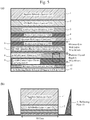
- the deep ultraviolet LED includes, sequentially from the top of the cross-sectional view in Fig. 1A (a-1), a sapphire substrate 1, an A1N buffer layer 2, an n-AlGaN layer 3, a barrier layer 4, a quantum well layer 5, a barrier layer 6, a multi-quantum barrier layer (MQB) 7, a p-AlGaN layer (transparent p-AlGaN layer) 8, a p-GaN contact layer 9, a Ni layer 10, and an Au reflecting electrode layer 11.
- MQB multi-quantum barrier layer
- the thickness of the p-AlGaN layer 8 is less than or equal to 100 nm, and a photonic crystal periodic structure 100 is provided in a region including the interface between the p-GaN contact layer 9 and the p-AlGaN layer 8 such that the photonic crystal periodic structure 100 does not extend beyond the p-AlGaN layer in the direction of the substrate.
- the photonic crystal periodic structure 100 is a reflecting photonic crystal periodic structure that is designed to reflect light with the wavelength ⁇ by having voids (columnar structures or holes) 101(h) and thus having a photonic band gap.
- the photonic crystal periodic structure is formed within only the p-GaN contact layer 9, light will be undesirably absorbed by the p-GaN contact layer.
- the multi-quantum barrier layer (MQB) 7 may also be an electron blocking layer. This is also true of the following embodiments.
- the reflecting photonic crystal periodic structure 100 has hole structures in which the voids 101(h) each having a columnar shape or the like, having a lower refractive index than those of the p-AlGaN layer and p-GaN contact layer, such as the air, and having a circular cross-section with a radius R, are formed in a triangular lattice pattern with a period of a along the x-direction and the y-direction.
- the voids 101(h) are structures that do not extend beyond the interface between the p-AlGaN layer 8 and the multi-quantum barrier layer 7.
- the distance G from end faces of the voids 101(h) in the direction of the substrate to the quantum well layer 5 is greater than or equal to the total thickness of the barrier layer 6 and the multi-quantum barrier layer 7 and less than or equal to 80 nm.
- the depth h of the reflecting photonic crystal periodic structure 100 is less than or equal to the total thickness of the p-AlGaN layer 8 and the p-GaN contact layer 9.
- TE light and TM light of deep ultraviolet light with a wavelength ⁇ emitted from the quantum well layer 5 are radiated in all directions and propagate through the medium while being elliptically polarized.
- the photonic crystal periodic structure 100 provided around the quantum well layer 5 is formed as two structures, which are the p-AlGaN layer 8 and the air, having different refractive indices on an end face.
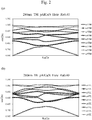
- a photonic band gap (PBG) for TM light was not observed, while as illustrated in Fig. 2(b) , a large PBG for TE light was observed between a first photonic band ( ⁇ 1TE) and a second photonic band ( ⁇ 2TE).
- PBG photonic band gap
- the photonic crystals are located closer to the quantum well layer, it becomes unnecessary to set the depths of the photonic crystals to 300 nm even when the period is 300 nm as described in Earlier Technology 1 or the like, and a reflection effect that is greater than or equal to the reflection effect of the structure of Earlier Technology 1 or the like can be obtained even when the depths of the photonic crystals are as shallow as about 60 nm. Further, the range of the order m that can be taken is increased. It should be noted that the smaller the m, the smaller the period.
- Figs. 3 illustrate views of the reflection effect of the photonic crystals.
- TE light that has entered the photonic crystal periodic structure provided around the quantum well layer from all directions is scattered within the plane and is reflected in the direction of the substrate as indicated by AR1 because the light completely satisfies the Bragg scattering condition.
- TM light will not be Bragg-scattered in the depth direction as indicated by a dashed line AR2 as there is no PBG for the TM light.
- the incident light will not be absorbed by the p-GaN contact layer or will not disappear.
- the deep ultraviolet LED in this embodiment it is possible to, by devising the position of the photonic crystal periodic structure provided in a target layer to be provided with the photonic crystal periodic structure, suppress the cloudiness of the crystal-forming layer without increasing the thickness thereof and increase the reflection effect, and thus obtain high light extraction efficiency.
- Figs. 4A (a-1) and 4A(a-2) are illustrated in accordance with the second embodiment.
- Fig. 4A (a-1) is a cross-sectional view and 4A(a-2) is a plan view.
- Fig. 4B(b) illustrates a deep ultraviolet LED mounted in a surface-mount package.
- the deep ultraviolet LED includes, sequentially from the top of Fig.
- a-1 a sapphire substrate 1, an A1N buffer layer 2, an n-AlGaN layer 3, a barrier layer 4, a quantum well layer 5, a barrier layer 6, a multi-quantum barrier layer (MQB) 7, a p-AlGaN contact layer (transparent p-AlGaN contact layer) 8a, an ultrathin Ni layer 10a, and an A1 reflecting electrode layer 11a.
- MQB multi-quantum barrier layer
- the thickness of the p-AlGaN contact layer 8a is less than or equal to 100 nm, and the photonic crystal periodic structure 100 is provided within the p-AlGaN contact layer 8a in a region in which the photonic crystal periodic structure 100 does not extend beyond the p-AlGaN layer in the direction of the substrate.
- the photonic crystal periodic structure 100 is a reflecting photonic crystal periodic structure that is designed to reflect light with the wavelength ⁇ by having voids (columnar structures or holes) 101(h) and thus having a photonic band gap.
- Figs. 4C (a-1), 4C(a-2), and 4D(b) illustrate modified examples of Figs. 4A (a-1), 4A(a-2), and 4B(b).
- This structure is the one in which the depths of the voids of the photonic crystal periodic structure in the thickness direction are extended in the direction opposite to the substrate such that the voids reach the reflecting electrode layer by penetrating the ultrathin metal layer, but do not penetrate the reflecting electrode layer.
- the other details of the photonic crystal periodic structure and observation of the views of TE light and TM light from the photonic band structure using the plane wave expansion method are the same as those in the first embodiment.
- light that has entered the photonic crystal periodic structure is scattered within the plane and is reflected in the direction of the substrate. Therefore, the light will not be absorbed by the A1 reflecting electrode (with a reflectivity of 90 %) or will not disappear.
- Figs. 5 illustrate a computation model (first embodiment, not according to the invention) of the photonic crystals in the p-GaN contact layer
- Figs. 6 illustrate a computation model (second embodiment, according to the invention) of the p-AlGaN contact layer.
- Fig. 7A illustrates a computation model of the pGaN contact.
- Fig. 7A (a-2) illustrates the analysis results and a radiation pattern.
- Fig. 7A(b) illustrates the details of the model and the light extraction efficiency that is analysis result.
- Fig. 7A (c-1) illustrates a computation model of the pAlGaN contact.
- Fig. 7A (c-2) illustrates the analysis results and a radiation pattern.
- Fig. 7B is a detailed process flow chart for determining the relationship between the size of the photonic band gap and the reflection/transmission effect as well as the rate of change of the light extraction efficiency (LEE) of the deep ultraviolet LED through analysis using the FDTD method, and obtaining the diameter d, the period a, and the depth h of the photonic crystals with which the LEE rate of change becomes maximum.
- LEE light extraction efficiency
- the ratio (R/a) of the period a and the radius R of the structure, which are parameters of the period structure, is tentatively determined.
- the refractive indices n 1 and n 2 of the structure are computed, and the average refractive index n av is computed from them and R/a, and then, the value is substituted into the formula of the Bragg condition to obtain the period a and the radius R for each order m.
- a photonic band structure for TE light is analyzed with the plane wave expansion method using R/a, the wavelength ⁇ , and the dielectric constants ⁇ 1 and ⁇ 2 of the structure obtained from the respective refractive indices n 1 and n 2 .
- R/a with which the PBG between the first photonic band and the second photonic band for TE light becomes maximum is determined through analysis that is repeatedly performed by changing the tentatively determined R/a value.
- the light extraction efficiency for light with the wavelength ⁇ is determined through a simulation analysis using the FDTD method that is performed by using as variables the individual period a and radius R corresponding to each order m of the Bragg condition and the depth h of a given period structure.
- Simulation using the FDTD method is repeatedly performed so as to determine the order m of the Bragg condition with which the light extraction efficiency for light with the wavelength ⁇ becomes maximum, as well as the period a, the radius R, and the depth h that are the parameters of the period structure corresponding to the order m.
- Tables 1 and 2 show the analysis results.
- Table 2 illustrates the analysis results of LEE when the order m is changed.
- pAlGaN photonic crystals in the p-AlGaN contact layer
- pGaN photonic crystals in the p-GaN contact layer
- Flat a structure without a photonic crystal periodic structure
- PhC Depth 40 nm the depths of the voids are 40 nm
- Power the output value of the FDTD method
- Flat LEE% the LEE value computed with the ray-tracing method
- Enhanced the LEE rate of change of the PhC output value relative to the output value of Flat
- PhC LEE% LEE% of photonic crystals that is Flat LEE% ⁇ (Enhanced+100%)
- G50 nm the distance from end faces of the voids to the quantum well layer is 50 nm
- Diameter the diameters of the voids
- Period the period of the photonic crystals.
- Figs. 8A are views illustrating electric field distribution Ex components; specifically, Fig. 8A(a) illustrates Flat, Fig. 8A(b) illustrates a photonic crystal periodic structure (the photonic crystal periodic structure is not illustrated), and Fig. 8A(c) illustrates a photonic crystal periodic structure (the photonic crystal periodic structure is illustrated). Each figure illustrates an electric field distribution in the cross-sectional structure. It should be noted that the photonic crystal periodic structure is omitted in Figs. 8A(c) and 8A(b) for clarification purposes.
- the results can verify that in the structure provided with a photonic crystal periodic structure, the reflection effect of the photonic crystals is obtained in the portion between the p-GaN contact layer and the Ni layer.
- a phenomenon similar to that of the Ex components in Figs. 8A are observed (see regions A3 and A4).
- Fig. 8D(a) illustrates an electric field distribution Etotal of Flat
- Fig. 8D(b) illustrates an electric field distribution Etotal of the center portion of the photonic crystals.
- an electric field propagates outward through repetition of high and low levels (shown by the gray scale of the color).
- the analysis results clearly illustrate a physical phenomenon that "TE light that has entered the photonic crystal periodic structure provided around the quantum well layer from all directions is scattered within the plane and is reflected in the direction of the substrate because the light completely satisfies the Bragg scattering condition" as has been described with reference to Figs. 3 .
- Figs. 9 illustrate the results of analyzing the LEE rate of change using the FDTD method.
- Fig. 9(a) illustrates the LEE rate of change of the photonic crystals in the p-AlGaN contact layer
- Fig. 9(b) illustrates the LEE rate of change of the photonic crystals in the p-GaN contact layer.
- FIG. 9(c) illustrates radiation patterns of the photonic crystal periodic structure in the p-GaN contact layer when the distance to the quantum well layer is 60 nm and the depths of the voids are 60 nm, and Flat of the layer, and similarly, radiation patterns of the photonic crystal periodic structure in the p-AlGaN contact layer and Flat of the layer.
- an output value in the front direction is particularly increased in comparison with that of Flat.
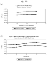
- Figs. 10 illustrate the results of analyzing the light extraction efficiency (LEE) obtained through cross simulation based on the FDTD method and the ray-tracing method.
- Fig. 10(a) illustrates the light extraction efficiency of the photonic crystals provided in the p-GaN contact layer and the p-AlGaN contact layer when the distance to the quantum well layer is 60 nm. From the results, a proportional relationship between the depth h of the photonic crystal periodic structure (holes) and the LEE is observed.
- the aforementioned results can confirm that as the photonic crystal periodic structure is located closer to the quantum well structure, the reflection effect of the photonic crystal periodic structure can be increased double in the case of the photonic crystal periodic structure provided in the p-AlGaN contact layer, and the light extraction efficiency of the photonic crystal periodic structure can be increased more than three times in the case of the photonic crystal periodic structure provided in the p-GaN contact layer.
- FIGS. 11 are views illustrating an exemplary process of forming a photonic crystal periodic structure.
- the nanoimprint lithography technique is used for forming photonic crystals.
- a resin mold 200 is used for the mold.
- bi-layer resist is used in order to perform dry etching in a direction close to vertical and accurately retain the diameters of holes.
- lower-layer resist 211 is formed on the surface of the p-GaN contact layer 209 through spin coating.
- Si-containing upper-layer resist 210 is formed thereon through spin coating to form bi-layer resist (see Fig. 11(a) ).
- the resin mold 200 having an inverted pattern of a predetermined photonic crystal periodic structure is pressed against the upper-layer resist, and is UV curing is performed to imprint a photonic crystal pattern 212 to the upper-layer resist 210 (see Fig. 11(b) ).
- the upper-layer resist 210 is etched with oxygen plasma to form a mask 213. See Fig. 11(c) .
- the mask 213 is etched with ICP plasma up to a position where the distance from an end face of the photonic crystal pattern (holes) 212 to the quantum well layer 205 becomes greater than or equal to the total thickness of the barrier layer 206 and the multi-quantum barrier layer 207 and less than or equal to 80 nm, which is also a position where the holes do not extend beyond the p-AlGaN layer 208, so that the depths of the holes are less than or equal to the total thickness of the p-AlGaN layer 208 and the p-GaN contact layer 209. See Fig. 11(d) . Finally, the remaining lower-layer resist 211 is washed to obtain a clean surface.
- a photonic crystal pattern is formed after a p-GaN contact layer or a p-AlGaN contact layer is formed, and then, a metal layer and a reflecting electrode layer are formed thereon using oblique deposition, so that a structure illustrated in Figs. 16A or 19A is formed.
- a metal layer and a reflecting electrode layer can be stacked on the surface of the p-GaN contact layer or the p-AlGaN contact layer without the metal layer and the reflecting electrode layer formed in the holes of the photonic crystal pattern.
- a structure of an AlGaN-based deep ultraviolet LED with a design wavelength ⁇ of 280 nm is represented in Fig. 12A (a-1) and 12A(a-2).
- Fig. 12A (a-1) is a cross-sectional view and Fig. 12A (a-2) is a plan view.
- Fig. 12B(b) is a deep ultraviolet LED mounted in a surface-mount package.
- This LED has the same structure as the stacked thin-film structure of the deep ultraviolet LED in the first embodiment, but is different in that the thickness of the p-GaN contact layer 9 is 200 nm. This is in order to obtain a planar surface by stacking a thick p-GaN contact layer in the device production process.
- the photonic crystal periodic structure 100 is provided in a region including the interface between the p-GaN contact layer 9 and the p-AlGaN layer 8 such that the photonic crystal periodic structure 100 does not extend beyond the p-AlGaN layer in the direction of the substrate.
- the photonic crystal periodic structure 100 is a reflecting photonic crystal periodic structure that is designed to reflect light with the wavelength ⁇ by having voids (columnar structures or holes) 101(h) and thus having a photonic band gap.
- the voids 101(h) are structures that do not extend beyond the interface between the p-AlGaN layer 8 and the multi-quantum barrier layer 7.
- the distance G from end faces of the voids 101(h) in the direction of the substrate to the quantum well layer 5 is greater than or equal to the total thickness of the barrier layer 6 and the multi-quantum barrier layer 7 and less than or equal to 80 nm.
- the depth h of the reflecting photonic crystal periodic structure 100 is less than or equal to the total thickness of the p-AlGaN layer 8 and the p-GaN contact layer 9.
- FIG. 13 illustrates a photonic crystal computation model of the p-GaN contact layer.
- Fig. 14(a) Enhancement of LEE
- Fig. 14(b) light extraction efficiency
- Fig. 14(c) radiation patterns.
- a maximum value which is greater than or equal to 2.5 times that of Flat, is obtained at all depths in the range of a distance of 50 nm from end faces of the voids to the quantum well layer.
- a structure provided with a photonic crystal periodic structure has an increased output value in the front direction (at an angle of 0 to 10°) relative to that of Flat.
- the efficiency is slightly decreased as the depths of the photonic crystals are greater.
- electric field intensity distributions in cross-sections of photonic crystals with depths of 120 nm, 140 nm, and 160 nm were compared.
- Fig. 15A illustrates an electric field intensity distribution in a cross-section of the photonic crystals with a depth of 120 nm.
- Fig. 15B illustrates an electric field intensity distribution in a cross-section of the photonic crystals with a depth of 140 nm.
- Fig. 15C illustrates an electric field intensity distribution in a cross-section of the photonic crystals with a depth of 160 nm. From Figs. 15A to 15C (electric field intensity distributions), it is seen that light (electric field) that has entered the photonic crystals with all depths reaches the deepest portions of the photonic crystals. This is considered to be due to the reason that as the photonic crystals have greater depths, light (electric field) enters the p-GaN contact layer, and the light is absorbed therein and thus disappears.
- the thickness of the p-GaN contact layer is preferably thinner so that the photonic crystals can have small depths.
- Figs. 16A (a-1) and 16A(a-2) illustrate the structure of an AlGaN-based deep ultraviolet LED with a design wavelength ⁇ of 280 nm as a deep ultraviolet LED in accordance with the fifth embodiment.
- Fig. 16A (a-1) is a cross-sectional view and Fig. 16A (a-2) is a plan view.
- Fig. 16B(b) illustrates a deep ultraviolet LED mounted in a surface-mount package.
- This LED has the same structure as the stacked thin-film structure of the deep ultraviolet LED in the fourth embodiment, but is different in that the thickness of the p-GaN contact layer 9 is 150 nm. This is a modified example seen from a perspective of using another method in the device production process.
- the photonic crystal periodic structure 100 is provided in a region including the interface between the p-GaN contact layer 9 and the p-AlGaN layer 8 such that the photonic crystal periodic structure 100 does not extend beyond the p-AlGaN layer in the direction of the substrate.
- the photonic crystal periodic structure 100 is a reflecting photonic crystal periodic structure that is designed to reflect light with the wavelength ⁇ by having voids (columnar structures or holes) 101(h) and thus having a photonic band gap.
- the voids 101(h) have structures in which the voids do not extend beyond the interface between the p-AlGaN layer 8 and the multi-quantum barrier layer 7 but reach the interface between the p-GaN contact layer 9 and the Ni layer 10.
- the distance G from end faces of the voids 101(h) in the direction of the substrate to the quantum well layer 5 is greater than or equal to the total thickness of the barrier layer 6 and the multi-quantum barrier layer 7 and less than or equal to 80 nm.
- the depth h of the reflecting photonic crystal periodic structure 100 is less than or equal to the total thickness of the p-AlGaN layer 8 and the p-GaN contact layer 9.
- FIG. 17 illustrate a photonic crystal computation model of the p-GaN contact layer.
- Fig. 18(a) Enhancement of LEE
- Fig. 18(b) light extraction efficiency
- Fig. 18(c) radiation patterns.
- a maximum value which is greater than or equal to 2.5 times that of Flat, is obtained at a distance of 60 nm from the quantum well layer 5. Meanwhile, regarding the light extraction efficiency in Fig. 18(b) , a maximum value of 15.7 % is obtained. Further, regarding the radiation patterns, an output on the axis (0 to 10°) is increased relative to that of Flat.
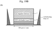
- Figs. 19A (a-1) and 19A(a-2) illustrate the structure of an AlGaN-based deep ultraviolet LED with a design wavelength ⁇ of 280 nm as a deep ultraviolet LED in accordance with the sixth embodiment.
- Fig. 19A (a-1) is a cross-sectional view and Fig. 19A (a-2) is a plan view.
- Fig. 19B(b) is a deep ultraviolet LED mounted in a surface-mount package.
- the LED has the same structure as the stacked thin-film structure of the deep ultraviolet LED in the second embodiment, but is a modified example seen from a perspective of using another method in the device production process.
- the thickness of the p-AlGaN contact layer 8a is less than or equal to 100 nm, and the photonic crystal periodic structure 100 is provided in a region within the p-AlGaN contact layer 8a such that the photonic crystal periodic structure 100 does not extend beyond the p-AlGaN contact layer in the direction of the substrate.
- the photonic crystal periodic structure 100 is a reflecting photonic crystal periodic structure that is designed to reflect light with the wavelength ⁇ by having voids (columnar structures or holes) 101(h) and thus having a photonic band gap.
- the voids 101(h) have structures in which the voids 101(h) do not extend beyond the interface between the p-AlGaN contact layer 8a and the multi-quantum barrier layer 7 but reach the interface between the p-AlGaN contact layer 8a and the ultrathin Ni layer 10a.
- the distance G of from end faces of the voids 101(h) in the direction of the substrate to the quantum well layer 5 is greater than or equal to the total thickness of the barrier layer 6 and the multi-quantum barrier layer 7 and less than or equal to 80 nm.
- the depth h of the reflecting photonic crystal periodic structure 100 is less than or equal to the thickness of the p-AlGaN contact layer 8a.
- FIG. 20 illustrate a photonic crystal computation model of the p-AlGaN contact layer.
- FIG. 21(a) Enhancement of LEE
- Fig. 21(b) LEE
- Fig. 21(c) radiation patterns.
- a maximum value which is 1.75 times that of Flat, is obtained at a distance of 50 nm from the quantum well layer 5. Meanwhile, regarding the light extraction efficiency in Fig. 21(b) , a maximum value of 23.0% is obtained. Further, regarding the radiation patterns in Fig. 21(c) , an output on the axis (0 to 10°) is increased relative to that of Flat.
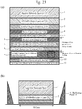
- Figs. 22A (a-1) and 22A(a-2) illustrate the structure of an AlGaN-based deep ultraviolet LED with a design wavelength ⁇ of 280 nm as a deep ultraviolet LED in accordance with the seventh embodiment.
- Fig. 22A (a-1) is a cross-sectional view and Fig. 22A (a-2) is a plan view.
- Fig. 22B(b) is a deep ultraviolet LED mounted in a surface-mount package.
- the LED has the same structure as the stacked thin-film structures of the deep ultraviolet LEDs in the first and forth embodiments, but is different in the position where the photonic crystal periodic structure 100 is provided. This is a modified example seen from a perspective of using another method in the device production process.
- the photonic crystal periodic structure 100 is provided in a region within the thickness of the p-GaN contact layer 9 such that the photonic crystal periodic structure 100 does not extend beyond the interface between the p-GaN contact layer 9 and the p-AlGaN layer 8 in the direction of the substrate.
- the photonic crystal periodic structure 100 is a reflecting photonic crystal periodic structure that is designed to reflect light with the wavelength ⁇ by having voids (columnar structures or holes) 101(h) and thus having a photonic band gap.
- the voids 101(h) are provided such that they do not extend beyond the interface between the p-GaN contact layer 9 and the Ni layer 10.
- the distance G from end faces of the voids 101(h) in the direction of the substrate to the quantum well layer 5 is greater than or equal to the total thickness of the barrier layer 6 and the multi-quantum barrier layer 7 and less than or equal to 80 nm.
- the depth h of the reflecting photonic crystal periodic structure 100 is less than or equal to the thickness of the p-GaN contact layer 9.
- TE light and TM light of deep ultraviolet light with a wavelength ⁇ emitted from the quantum well layer 5 are radiated in all directions and propagate through the medium while being elliptically polarized.
- the photonic crystal periodic structure 100 provided around the quantum well layer 5 is provided within the thickness of the p-GaN contact layer 9. Therefore, the photonic crystal periodic structure 100 is formed as a structure having two different refractive indices, which are the p-GaN contact layer 9 and the air, at an end face thereof.
- FIG. 23 illustrate a photonic crystal computation model of the LED structure.
- the computation model was designed such that the thickness of the p-AlGaN layer 8 was changed in increments of 10 nm in the range of 0 to 30 nm, and the positions of the voids 101(h) were set such that end faces of the voids in the direction of the substrate had depths of 120 nm from the interface between the p-AlGaN layer 8 and the p-GaN contact layer 9.
- the thinner the p-AlGaN layer 8 the shorter the distance G between the quantum well layer 5 and the end faces of the voids 101(h) in the direction of the substrate. That is, the computation model was designed such that the distance G became 50 nm when the thickness of the p-AlGaN layer 8 was 0 nm, and the thickness of the p-AlGaN layer 8 was changed in increments of 10 nm so that the distance G similarly became 80 nm when the thickness of the p-AlGaN layer 8 was 30 nm.
- the analysis results are shown in Table 6, Fig. 24(a) : Enhancement of LEE, Fig. 24(b) : light extraction efficiency, and Fig.
- a maximum value which is about 2.7 times as high, is obtained at a distance G of 50 nm from the quantum well layer 5 (the thickness of the p-AlGaN layer in this case is 0 nm), and an intensity, which is about 2.5 times as high, is also obtained at a distance G of 60 nm (likewise, the thickness of the p-AlGaN layer is 10 nm).
- a maximum value of 17.3% is obtained at a distance G of 50 nm.
- Fig. 24(c) illustrates radiation patterns at a distance G of 50 nm. It is found that an output in the axial direction (0 to 30°) is increased relative to that of Flat.
- an LED device is formed.
- the LEE of the deep ultraviolet LED can be drastically improved by providing a photonic crystal periodic structure in a thin p-AlGaN layer.
Landscapes
- Led Devices (AREA)
Claims (4)
- LED für den tief-ultravioletten Spektralbereich mit einer Auslegungswellenlänge λ, die, aufeinanderfolgend von einer Seite gegenüber einem Substrat (1) angeordnet, eine reflektierende Elektrodenschicht (11a), eine Metallschicht (10a), eine p-AlGaN-Kontaktschicht (8a), die für Licht mit der Wellenlänge λ durchlässig ist, eine aus einer Multiquanten-Barriereschicht (7) oder einer Elektronenblockierschicht, eine Barriereschicht (6) und eine Quantentopfschicht (5) umfasst,
wobei:eine Dicke der p-AlGaN-Kontaktschicht (8a) kleiner oder gleich 100 nm ist,eine reflektierende photonische periodische Kristallstruktur (100), die mehrere Hohlräume (101) aufweist, innerhalb der p-AlGaN-Kontaktschicht (8a) in einem Bereich in einer Dickenrichtung vorgesehen ist, in dem sich die reflektierende photonische periodische Kristallstruktur (100) nicht über die p-AlGaN-Kontaktschicht (8a) in einer Richtung des Substrats (1) hinaus erstreckt,um eine maximale Lichtextraktionseffizienz zu erhalten, ein Abstand von Endflächen der Hohlräume (101) in der Richtung des Substrats (1) zu der Quantentopfschicht (5) größer oder gleich einer Gesamtdicke aus der Barriereschicht (6) und der Multiquanten-Barriereschicht (7) oder der Elektronenblockierschicht und kleiner oder gleich 80 nm ist und eine Tiefe h jedes Hohlraums (101) kleiner oder gleich der Dicke der p-AlGaN-Kontaktschicht (8a) ist,die reflektierende photonische periodische Kristallstruktur (100) eine photonische Bandlücke aufweist, die für TE-polarisierte Komponenten öffnet,eine Periode a der photonischen periodischen Kristallstruktur (100) eine Bragg-Bedingung in Bezug auf Licht mit der Auslegungswellenlänge λ erfüllt,eine Ordnung m in einer Formel der Bragg-Bedingung 1≤m≤5 erfüllt, und, vorausgesetzt, dass ein Radius jedes Hohlraums R ist, R/a, womit die photonische Bandlücke maximal wird, erfüllt ist. - LED für den tief-ultravioletten Spektralbereich mit einer Auslegungswellenlänge λ, die, aufeinanderfolgend von einer Seite gegenüber einem Substrat (1) angeordnet, eine reflektierende Elektrodenschicht (11), eine Metallschicht (10), eine p-GaN-Kontaktschicht (9), eine p-AlGaN-Schicht (8), die für Licht mit der Wellenlänge λ durchlässig ist, eine aus einer Multiquanten-Barriereschicht (7) oder einer Elektronenblockierschicht, eine Barriereschicht (6) und eine Quantentopfschicht (5) umfasst,
wobei:eine Dicke der p-AlGaN-Schicht (8) kleiner als 100 nm ist,eine reflektierende photonische periodische Kristallstruktur (100), die mehrere Hohlräume (101) aufweist, in einem Bereich innerhalb einer Dicke der p-GaN-Kontaktschicht (9) in einer Richtung des Substrats (1) derart vorgesehen ist, dass sich die reflektierende photonische periodische Kristallstruktur (100) nicht über eine Schnittstelle zwischen der p-GaN-Kontaktschicht (9) und der p-AlGaN-Schicht (8) hinaus erstreckt,um eine maximale Lichtextraktionseffizienz zu erhalten, ein Abstand von Endflächen der Hohlräume (101) in der Richtung des Substrats (1) zu der Quantentopfschicht (5) größer als eine Gesamtdicke aus der Barriereschicht (6) und der Multiquanten-Barriereschicht (7) oder der Elektronenblockierschicht und kleiner oder gleich 80 nm ist und eine Tiefe h jedes Hohlraums (101) kleiner oder gleich der Dicke der p-GaN-Kontaktschicht (9) ist,die reflektierende photonische periodische Kristallstruktur (100) eine photonische Bandlücke aufweist, die für TE-polarisierte Komponenten öffnet,eine Periode a der photonischen periodischen Kristallstruktur (100) eine Bragg-Bedingung in Bezug auf Licht mit der Auslegungswellenlänge λ erfüllt,eine Ordnung m in einer Formel der Bragg-Bedingung 1≤m≤5 erfüllt und, vorausgesetzt, dass ein Radius jedes Hohlraums R ist, R/a, womit die photonische Bandlücke maximal wird, erfüllt ist. - Verfahren zum Herstellen der LED für den tief-ultravioletten Spektralbereich nach Anspruch 1, umfassend:Vorbereiten einer gestapelten Struktur, die, aufeinanderfolgend von einer Seite gegenüber einem Substrat (1) angeordnet, eine reflektierende Elektrodenschicht (11a), eine Metallschicht (10a) und eine p-AlGaN-Kontaktschicht (8a), die für Licht mit der Wellenlänge λ durchlässig ist, aufweist;Vorbereiten einer Form zum Bilden einer reflektierenden photonischen periodischen Kristallstruktur (100), wobei:eine Dicke der p-AlGaN-Kontaktschicht (8a) kleiner oder gleich 100 nm ist,die reflektierende photonische periodische Kristallstruktur (100) mehrere Hohlräume (101) aufweist und in einem Bereich in einer Dickenrichtung innerhalb der p-AlGaN-Kontaktschicht (8a) derart vorgesehen ist, dass sich die reflektierende photonische periodische Kristallstruktur (100) nicht über die p-AlGaN-Schicht (8a) in einer Richtung des Substrats hinaus erstreckt, undum eine maximale Lichtextraktionseffizienz zu erhalten, ein Abstand von Endflächen der Hohlräume (101) in der Richtung des Substrats (1) zu der Quantentopfschicht (5) größer oder gleich einer Gesamtdicke aus der Barriereschicht (6) und der Multiquanten-Barriereschicht (7) oder der Elektronenblockierschicht und kleiner oder gleich 80 nm ist und eine Tiefe h jedes Hohlraums (101) kleiner oder gleich einer Dicke der p-AlGaN-Kontaktschicht (8a) ist;Bilden einer Resistschicht auf der gestapelten Struktur und Abdrücken einer Struktur der Form darauf; undnachfolgendes Ätzen der gestapelten Struktur unter Verwendung der Resistschicht als Maske, wodurch die photonische periodische Kristallstruktur (100) gebildet wird.
- Verfahren zum Herstellen der LED für den tief-ultravioletten Spektralbereich nach Anspruch 2, umfassend:Vorbereiten einer gestapelten Struktur, die, aufeinanderfolgend von einer Seite gegenüber einem Substrat (1) angeordnet, eine reflektierende Elektrodenschicht (11), eine Metallschicht (10), eine p-GaN-Kontaktschicht (8) und eine p-AlGaN-Schicht (8), die für Licht mit der Wellenlänge λ durchlässig ist, aufweist;Vorbereiten einer Form zum Bilden einer reflektierenden photonischen periodischen Kristallstruktur (100), wobei:eine Dicke der p-AlGaN-Schicht (8) kleiner als 100 nm ist,die reflektierende photonische periodische Kristallstruktur (100) mehrere Hohlräume (101) aufweist und in einem Bereich innerhalb einer Dicke der p-GaN-Kontaktschicht (9) in einer Richtung des Substrats (1) derart vorgesehen ist, dass sich die reflektierende photonische periodische Kristallstruktur (100) nicht über eine Schnittstelle zwischen der p-GaN-Kontaktschicht (9) und der p-AlGaN-Schicht (8) hinaus erstreckt, undum eine maximale Lichtextraktionseffizienz zu erhalten, ein Abstand von Endflächen der Hohlräume (101) in der Richtung des Substrats (1) zu der Quantentopfschicht (5) größer als eine Gesamtdicke aus der Barriereschicht (6) und der Multiquanten-Barriereschicht (7) oder der Elektronenblockierschicht und kleiner oder gleich 80 nm ist und eine Tiefe h jedes Hohlraums (101) kleiner oder gleich der Dicke der p-GaN-Kontaktschicht (9) ist;Züchten von Kristallen bis zu der p-GaN-Kontaktschicht (9) der gestapelten Struktur, Bilden einer Resistschicht darauf und Abdrücken einer Struktur der Form darauf; undnachfolgendes Ätzen der gestapelten Struktur unter Verwendung der Resistschicht als Maske, wodurch die photonische periodische Kristallstruktur (101) gebildet wird.
Applications Claiming Priority (2)
| Application Number | Priority Date | Filing Date | Title |
|---|---|---|---|
| JP2016069434 | 2016-03-30 | ||
| PCT/JP2016/082397 WO2017168811A1 (ja) | 2016-03-30 | 2016-11-01 | 深紫外led及びその製造方法 |
Publications (3)
| Publication Number | Publication Date |
|---|---|
| EP3249701A1 EP3249701A1 (de) | 2017-11-29 |
| EP3249701A4 EP3249701A4 (de) | 2017-11-29 |
| EP3249701B1 true EP3249701B1 (de) | 2020-07-08 |
Family
ID=59014415
Family Applications (1)
| Application Number | Title | Priority Date | Filing Date |
|---|---|---|---|
| EP16861100.2A Active EP3249701B1 (de) | 2016-03-30 | 2016-11-01 | Led für den tief-ultravioletten spektralbereich und verfahren zu ihrer herstellung |
Country Status (6)
| Country | Link |
|---|---|
| US (1) | US10056526B2 (de) |
| EP (1) | EP3249701B1 (de) |
| KR (1) | KR101811819B1 (de) |
| CN (1) | CN107534072B (de) |
| TW (1) | TWI634674B (de) |
| WO (1) | WO2017168811A1 (de) |
Families Citing this family (10)
| Publication number | Priority date | Publication date | Assignee | Title |
|---|---|---|---|---|
| US10680134B2 (en) * | 2015-09-03 | 2020-06-09 | Marubun Corporation | Deep ultraviolet LED and method for manufacturing the same |
| US11309454B2 (en) | 2018-01-26 | 2022-04-19 | Marubun Corporation | Deep ultraviolet LED and method for producing the same |
| CN110197839B (zh) * | 2018-06-15 | 2021-08-03 | 京东方科技集团股份有限公司 | 双面显示面板及其制备方法、双面显示装置 |
| TW202027304A (zh) * | 2018-08-24 | 2020-07-16 | 日商丸文股份有限公司 | 深紫外led裝置及其製造方法 |
| JP2020107778A (ja) * | 2018-12-28 | 2020-07-09 | 丸文株式会社 | 深紫外led装置及びその製造方法 |
| JP2021097148A (ja) * | 2019-12-18 | 2021-06-24 | 日機装株式会社 | 半導体発光素子 |
| CN111106212A (zh) * | 2019-12-26 | 2020-05-05 | 南京亮芯信息科技有限公司 | 垂直结构深紫外发光二极管及其制备方法 |
| JP6814902B1 (ja) * | 2020-04-24 | 2021-01-20 | 日機装株式会社 | 半導体発光素子および半導体発光素子の製造方法 |
| CN118156389B (zh) * | 2024-05-13 | 2024-08-02 | 江西乾照光电有限公司 | 一种白光led外延片、外延生长方法及led芯片 |
| CN121710049B (zh) * | 2026-02-13 | 2026-04-24 | 山东省科学院激光研究所 | 一种基于环形光子晶体的芯片及其制备方法 |
Family Cites Families (78)
| Publication number | Priority date | Publication date | Assignee | Title |
|---|---|---|---|---|
| US5337328A (en) | 1992-05-08 | 1994-08-09 | Sdl, Inc. | Semiconductor laser with broad-area intra-cavity angled grating |
| US5955749A (en) | 1996-12-02 | 1999-09-21 | Massachusetts Institute Of Technology | Light emitting device utilizing a periodic dielectric structure |
| EP1378949A4 (de) | 2001-03-21 | 2006-03-22 | Mitsubishi Cable Ind Ltd | Lichtemittierendes halbleiterbauelement |
| JP3991612B2 (ja) | 2001-04-09 | 2007-10-17 | 日亜化学工業株式会社 | 発光素子 |
| US6936854B2 (en) | 2001-05-10 | 2005-08-30 | Canon Kabushiki Kaisha | Optoelectronic substrate |
| WO2003034113A2 (en) | 2001-10-19 | 2003-04-24 | Nkt Research & Innovation A/S | Integrated photonic crystal structure and method of producing same |
| JP4329374B2 (ja) | 2002-07-29 | 2009-09-09 | パナソニック電工株式会社 | 発光素子およびその製造方法 |
| US6878969B2 (en) | 2002-07-29 | 2005-04-12 | Matsushita Electric Works, Ltd. | Light emitting device |
| JP2004200209A (ja) | 2002-12-16 | 2004-07-15 | Fuji Xerox Co Ltd | 電極等の導電パターンの形成方法およびこれを用いた面発光型半導体レーザ並びにその製造方法 |
| JP4610863B2 (ja) | 2003-03-19 | 2011-01-12 | フィリップス ルミレッズ ライティング カンパニー リミテッド ライアビリティ カンパニー | フォトニック結晶構造を使用するled効率の改良 |
| JP4317375B2 (ja) | 2003-03-20 | 2009-08-19 | 株式会社日立製作所 | ナノプリント装置、及び微細構造転写方法 |
| US7083993B2 (en) | 2003-04-15 | 2006-08-01 | Luminus Devices, Inc. | Methods of making multi-layer light emitting devices |
| US7367691B2 (en) | 2003-06-16 | 2008-05-06 | Industrial Technology Research Institute | Omnidirectional one-dimensional photonic crystal and light emitting device made from the same |
| WO2005008791A2 (en) | 2003-07-16 | 2005-01-27 | Matsushita Electric Industrial Co., Ltd. | Semiconductor light emitting device, method of manufacturing the same, and lighting apparatus and display apparatus using the same |
| US7012279B2 (en) | 2003-10-21 | 2006-03-14 | Lumileds Lighting U.S., Llc | Photonic crystal light emitting device |
| US20070267646A1 (en) | 2004-06-03 | 2007-11-22 | Philips Lumileds Lighting Company, Llc | Light Emitting Device Including a Photonic Crystal and a Luminescent Ceramic |
| JP2008521211A (ja) | 2004-07-24 | 2008-06-19 | ヨン ラグ ト | 二次元ナノ周期構造体を有する薄膜蛍光体を備えるled装置 |
| US20060043400A1 (en) | 2004-08-31 | 2006-03-02 | Erchak Alexei A | Polarized light emitting device |
| JP2006196658A (ja) | 2005-01-13 | 2006-07-27 | Matsushita Electric Ind Co Ltd | 半導体発光素子およびその製造方法 |
| JP2006276388A (ja) | 2005-03-29 | 2006-10-12 | Alps Electric Co Ltd | フォトニック結晶スラブ及びフォトニック結晶導波路と光デバイス |
| WO2006116030A2 (en) | 2005-04-21 | 2006-11-02 | Aonex Technologies, Inc. | Bonded intermediate substrate and method of making same |
| JP4027393B2 (ja) * | 2005-04-28 | 2007-12-26 | キヤノン株式会社 | 面発光レーザ |
| WO2006138465A2 (en) | 2005-06-17 | 2006-12-28 | Goldeneye, Inc. | Light emitting diodes with reflective electrode and side electrode |
| US8163575B2 (en) | 2005-06-17 | 2012-04-24 | Philips Lumileds Lighting Company Llc | Grown photonic crystals in semiconductor light emitting devices |
| TWI253771B (en) | 2005-07-25 | 2006-04-21 | Formosa Epitaxy Inc | Light emitting diode structure |
| JP2007109689A (ja) | 2005-10-11 | 2007-04-26 | Seiko Epson Corp | 発光素子、発光素子の製造方法及び画像表示装置 |
| US7679098B2 (en) | 2006-01-30 | 2010-03-16 | Avago Technologies Ecbu Ip (Singapore) Pte. Ltd. | Highly directional light emitting diode using photonic bandgap waveguides |
| US7687811B2 (en) | 2006-03-21 | 2010-03-30 | Lg Electronics Inc. | Vertical light emitting device having a photonic crystal structure |
| JP2007294789A (ja) | 2006-04-27 | 2007-11-08 | Sony Corp | 半導体レーザ素子 |
| KR100736623B1 (ko) | 2006-05-08 | 2007-07-09 | 엘지전자 주식회사 | 수직형 발광 소자 및 그 제조방법 |
| JP4231880B2 (ja) | 2006-07-26 | 2009-03-04 | 株式会社東芝 | 3次元構造体およびそれを有する発光素子ならびにその製造方法 |
| JP2008053425A (ja) | 2006-08-24 | 2008-03-06 | Matsushita Electric Ind Co Ltd | 半導体発光装置 |
| US7829905B2 (en) | 2006-09-07 | 2010-11-09 | Hong Kong Applied Science And Technology Research Institute Co., Ltd. | Semiconductor light emitting device |
| US7697584B2 (en) | 2006-10-02 | 2010-04-13 | Philips Lumileds Lighting Company, Llc | Light emitting device including arrayed emitters defined by a photonic crystal |
| JP2008098526A (ja) | 2006-10-13 | 2008-04-24 | Toyoda Gosei Co Ltd | 発光素子 |
| JP2008117922A (ja) * | 2006-11-02 | 2008-05-22 | Yamaguchi Univ | 半導体発光素子及びその製造方法 |
| KR100886821B1 (ko) | 2007-05-29 | 2009-03-04 | 한국광기술원 | 전기적 특성을 향상한 광자결정 발광 소자 및 제조방법 |
| JP2008311317A (ja) | 2007-06-12 | 2008-12-25 | Eudyna Devices Inc | 半導体発光素子 |
| KR101341374B1 (ko) | 2007-07-30 | 2013-12-16 | 삼성전자주식회사 | 광자결정 발광소자 및 그 제조방법 |
| JP4408443B2 (ja) | 2007-08-01 | 2010-02-03 | 株式会社日立製作所 | 回転電機 |
| JP2009267263A (ja) | 2008-04-28 | 2009-11-12 | Kyocera Corp | 発光装置およびその製造方法 |
| KR100933529B1 (ko) | 2008-05-28 | 2009-12-23 | 재단법인서울대학교산학협력재단 | 광자결정 구조체를 구비한 발광소자 |
| JPWO2009148138A1 (ja) | 2008-06-05 | 2011-11-04 | 旭硝子株式会社 | ナノインプリント用モールド、その製造方法および表面に微細凹凸構造を有する樹脂成形体ならびにワイヤグリッド型偏光子の製造方法 |
| JP5282503B2 (ja) | 2008-09-19 | 2013-09-04 | 日亜化学工業株式会社 | 半導体発光素子 |
| JP5379434B2 (ja) | 2008-09-22 | 2013-12-25 | 学校法人 名城大学 | 発光素子用サファイア基板の製造方法 |
| JP4892025B2 (ja) | 2008-09-26 | 2012-03-07 | 株式会社東芝 | インプリント方法 |
| KR101040462B1 (ko) | 2008-12-04 | 2011-06-09 | 엘지이노텍 주식회사 | 발광 소자 및 그 제조방법 |
| KR20110106287A (ko) | 2008-12-05 | 2011-09-28 | 아사히 가라스 가부시키가이샤 | 광경화성 조성물 및 표면에 미세 패턴을 갖는 성형체의 제조 방법 |
| GB0902569D0 (en) | 2009-02-16 | 2009-04-01 | Univ Southampton | An optical device |
| KR100999713B1 (ko) | 2009-03-17 | 2010-12-08 | 엘지이노텍 주식회사 | 발광소자 및 그 제조방법 |
| JP5300078B2 (ja) | 2009-10-19 | 2013-09-25 | 国立大学法人京都大学 | フォトニック結晶発光ダイオード |
| US9028070B2 (en) | 2009-10-23 | 2015-05-12 | Nec Corporation | Light emitting element having structural bodies arrayed at a first pitch along a first direction and arrayed at a second pitch different from said first pitch along a second direction and projection display device provided with same |
| DE102009057780A1 (de) | 2009-12-10 | 2011-06-16 | Osram Opto Semiconductors Gmbh | Optoelektronisches Halbleiterbauteil und photonischer Kristall |
| US8759813B2 (en) | 2010-02-24 | 2014-06-24 | Riken | Light-emitting element having nitride semiconductor multiquantum barrier, and process for production thereof |
| JP5549338B2 (ja) | 2010-04-09 | 2014-07-16 | ウシオ電機株式会社 | 紫外光放射用窒素化合物半導体ledおよびその製造方法 |
| JP5331051B2 (ja) | 2010-04-21 | 2013-10-30 | パナソニック株式会社 | 発光素子 |
| US8907322B2 (en) | 2010-06-18 | 2014-12-09 | Sensor Electronic Technology, Inc. | Deep ultraviolet light emitting diode |
| US9130348B2 (en) | 2010-07-30 | 2015-09-08 | Kyoto University | Two-dimensional photonic crystal laser |
| US9103527B2 (en) | 2010-11-18 | 2015-08-11 | Nec Corporation | Light source unit and projection display device with the same |
| JP5620827B2 (ja) | 2011-01-06 | 2014-11-05 | 富士フイルム株式会社 | ナノインプリントモールドの洗浄方法 |
| KR20120092326A (ko) * | 2011-02-11 | 2012-08-21 | 서울옵토디바이스주식회사 | 광 결정 구조를 갖는 비극성 발광 다이오드 및 그것을 제조하는 방법 |
| KR20120092325A (ko) | 2011-02-11 | 2012-08-21 | 서울옵토디바이스주식회사 | 광 결정 구조를 갖는 발광 다이오드 및 그것을 제조하는 방법 |
| JP5678728B2 (ja) | 2011-03-03 | 2015-03-04 | 大日本印刷株式会社 | モールドおよびその製造方法 |
| JP2012186414A (ja) | 2011-03-08 | 2012-09-27 | Toshiba Corp | 発光装置 |
| JP5715686B2 (ja) | 2011-03-23 | 2015-05-13 | 創光科学株式会社 | 窒化物半導体紫外線発光素子 |
| CN104210047B (zh) | 2011-06-23 | 2016-09-28 | 旭化成株式会社 | 微细图案形成用积层体及微细图案形成用积层体的制造方法 |
| US20130009167A1 (en) | 2011-07-06 | 2013-01-10 | Sharp Kabushiki Kaisha | Light emitting diode with patterned structures and method of making the same |
| EP2733752B1 (de) | 2011-07-12 | 2016-10-05 | Marubun Corporation | Lichtemittierendes element und verfahren zu dessen herstellung |
| JP2013042079A (ja) | 2011-08-19 | 2013-02-28 | Sharp Corp | 半導体発光装置 |
| JP2013120829A (ja) * | 2011-12-07 | 2013-06-17 | Sharp Corp | 窒化物半導体紫外発光素子 |
| CN103597619B (zh) | 2012-03-07 | 2015-10-14 | 株式会社爱发科 | 制造装置的方法 |
| US20150044417A1 (en) | 2012-03-12 | 2015-02-12 | Asahi Kasei E-Materials Corporation | Mold, resist layered product, manufacturing method of the product, and concavo-convex structure product |
| KR102059030B1 (ko) | 2012-09-24 | 2019-12-24 | 엘지이노텍 주식회사 | 자외선 발광 소자 |
| CN103165771B (zh) | 2013-03-28 | 2015-07-15 | 天津三安光电有限公司 | 一种具有埋入式孔洞结构的氮化物底层及其制备方法 |
| CN105283968A (zh) * | 2013-07-17 | 2016-01-27 | 丸文株式会社 | 半导体发光元件及其制造方法 |
| JP2015041763A (ja) | 2013-08-20 | 2015-03-02 | 正幸 安部 | 光半導体装置及びその製造方法 |
| JP5757512B1 (ja) | 2014-03-06 | 2015-07-29 | 丸文株式会社 | 深紫外led及びその製造方法 |
| JP5999800B1 (ja) | 2015-01-16 | 2016-09-28 | 丸文株式会社 | 深紫外led及びその製造方法 |
-
2016
- 2016-11-01 EP EP16861100.2A patent/EP3249701B1/de active Active
- 2016-11-01 CN CN201680003179.3A patent/CN107534072B/zh active Active
- 2016-11-01 KR KR1020177013240A patent/KR101811819B1/ko active Active
- 2016-11-01 US US15/526,860 patent/US10056526B2/en active Active
- 2016-11-01 WO PCT/JP2016/082397 patent/WO2017168811A1/ja not_active Ceased
-
2017
- 2017-02-03 TW TW106103640A patent/TWI634674B/zh active
Non-Patent Citations (1)
| Title |
|---|
| None * |
Also Published As
| Publication number | Publication date |
|---|---|
| EP3249701A1 (de) | 2017-11-29 |
| EP3249701A4 (de) | 2017-11-29 |
| TW201735393A (zh) | 2017-10-01 |
| KR101811819B1 (ko) | 2017-12-22 |
| TWI634674B (zh) | 2018-09-01 |
| US10056526B2 (en) | 2018-08-21 |
| CN107534072A (zh) | 2018-01-02 |
| WO2017168811A1 (ja) | 2017-10-05 |
| CN107534072B (zh) | 2019-04-19 |
| US20180198026A1 (en) | 2018-07-12 |
Similar Documents
| Publication | Publication Date | Title |
|---|---|---|
| EP3249701B1 (de) | Led für den tief-ultravioletten spektralbereich und verfahren zu ihrer herstellung | |
| US9349918B2 (en) | Light emitting element and method for manufacturing same | |
| US10811577B2 (en) | Semiconductor light emitting element and method for manufacturing the same | |
| US11309454B2 (en) | Deep ultraviolet LED and method for producing the same | |
| US10950751B2 (en) | Deep ultraviolet LED and method for manufacturing the same | |
| KR101862500B1 (ko) | 광학 기판, 반도체 발광 소자 및 반도체 발광 소자의 제조 방법 | |
| KR101580619B1 (ko) | 반도체 발광 소자 및 제조 방법 | |
| CN101421889B (zh) | 具有用于衍射导波的光子晶体镜的vcsel | |
| EP3246956A1 (de) | Tiefultraviolett-led und verfahren zur herstellung davon | |
| EP2942818A1 (de) | Tiefultraviolett-led und verfahren zur herstellung davon | |
| JP6156898B1 (ja) | 深紫外led及びその製造方法 | |
| CN102138229B (zh) | 光电子半导体芯片 | |
| KR100867499B1 (ko) | 질화물 반도체 발광소자 및 그 제조방법 | |
| Chavoor et al. | Light extraction improvement of GaN LEDs using nano-scale top transmission gratings | |
| WO2018025805A1 (ja) | 半導体発光素子及びその製造方法 | |
| Lee et al. | Nanophotonics of Hexagonal Lattice GaN Crystals Fabricated using an Electron Beam Nanolithography Process | |
| Feng et al. | Theoretical analysis of enhanced light output from a GaN light emitting diode with an embedded photonic crystal |
Legal Events
| Date | Code | Title | Description |
|---|---|---|---|
| STAA | Information on the status of an ep patent application or granted ep patent |
Free format text: STATUS: UNKNOWN |
|
| STAA | Information on the status of an ep patent application or granted ep patent |
Free format text: STATUS: THE INTERNATIONAL PUBLICATION HAS BEEN MADE |
|
| PUAI | Public reference made under article 153(3) epc to a published international application that has entered the european phase |
Free format text: ORIGINAL CODE: 0009012 |
|
| STAA | Information on the status of an ep patent application or granted ep patent |
Free format text: STATUS: REQUEST FOR EXAMINATION WAS MADE |
|
| 17P | Request for examination filed |
Effective date: 20170512 |
|
| A4 | Supplementary search report drawn up and despatched |
Effective date: 20170717 |
|
| AK | Designated contracting states |
Kind code of ref document: A1 Designated state(s): AL AT BE BG CH CY CZ DE DK EE ES FI FR GB GR HR HU IE IS IT LI LT LU LV MC MK MT NL NO PL PT RO RS SE SI SK SM TR |
|
| AX | Request for extension of the european patent |
Extension state: BA ME |
|
| STAA | Information on the status of an ep patent application or granted ep patent |
Free format text: STATUS: EXAMINATION IS IN PROGRESS |
|
| 17Q | First examination report despatched |
Effective date: 20180523 |
|
| DAV | Request for validation of the european patent (deleted) | ||
| DAX | Request for extension of the european patent (deleted) | ||
| RIC1 | Information provided on ipc code assigned before grant |
Ipc: H01L 33/40 20100101ALN20191219BHEP Ipc: H01L 33/32 20100101ALI20191219BHEP Ipc: H01L 33/10 20100101AFI20191219BHEP |
|
| GRAP | Despatch of communication of intention to grant a patent |
Free format text: ORIGINAL CODE: EPIDOSNIGR1 |
|
| STAA | Information on the status of an ep patent application or granted ep patent |
Free format text: STATUS: GRANT OF PATENT IS INTENDED |
|
| RIC1 | Information provided on ipc code assigned before grant |
Ipc: H01L 33/10 20100101AFI20200109BHEP Ipc: H01L 33/32 20100101ALI20200109BHEP Ipc: H01L 33/40 20100101ALN20200109BHEP |
|
| INTG | Intention to grant announced |
Effective date: 20200129 |
|
| GRAS | Grant fee paid |
Free format text: ORIGINAL CODE: EPIDOSNIGR3 |
|
| GRAA | (expected) grant |
Free format text: ORIGINAL CODE: 0009210 |
|
| STAA | Information on the status of an ep patent application or granted ep patent |
Free format text: STATUS: THE PATENT HAS BEEN GRANTED |
|
| AK | Designated contracting states |
Kind code of ref document: B1 Designated state(s): AL AT BE BG CH CY CZ DE DK EE ES FI FR GB GR HR HU IE IS IT LI LT LU LV MC MK MT NL NO PL PT RO RS SE SI SK SM TR |
|
| REG | Reference to a national code |
Ref country code: CH Ref legal event code: EP Ref country code: AT Ref legal event code: REF Ref document number: 1289408 Country of ref document: AT Kind code of ref document: T Effective date: 20200715 |
|
| REG | Reference to a national code |
Ref country code: DE Ref legal event code: R096 Ref document number: 602016039762 Country of ref document: DE |
|
| REG | Reference to a national code |
Ref country code: IE Ref legal event code: FG4D |
|
| REG | Reference to a national code |
Ref country code: DE Ref legal event code: R082 Ref document number: 602016039762 Country of ref document: DE Representative=s name: GLEISS GROSSE SCHRELL UND PARTNER MBB PATENTAN, DE Ref country code: DE Ref legal event code: R081 Ref document number: 602016039762 Country of ref document: DE Owner name: MARUBUN CORPORATION, JP Free format text: FORMER OWNERS: MARUBUN CORPORATION, TOKYO, JP; RIKEN, WAKO-SHI, SAITAMA, JP; TOKYO OHKA KOGYO CO., LTD., KAWASAKI-SHI, JP; TOSHIBA KIKAI KABUSHIKI KAISHA, TOKYO, JP; ULVAC, INC., CHIGASAKI-SHI, KANAGAWA, JP Ref country code: DE Ref legal event code: R081 Ref document number: 602016039762 Country of ref document: DE Owner name: ULVAC, INC., CHIGASAKI-SHI, JP Free format text: FORMER OWNERS: MARUBUN CORPORATION, TOKYO, JP; RIKEN, WAKO-SHI, SAITAMA, JP; TOKYO OHKA KOGYO CO., LTD., KAWASAKI-SHI, JP; TOSHIBA KIKAI KABUSHIKI KAISHA, TOKYO, JP; ULVAC, INC., CHIGASAKI-SHI, KANAGAWA, JP Ref country code: DE Ref legal event code: R081 Ref document number: 602016039762 Country of ref document: DE Owner name: TOKYO OHKA KOGYO CO., LTD., JP Free format text: FORMER OWNERS: MARUBUN CORPORATION, TOKYO, JP; RIKEN, WAKO-SHI, SAITAMA, JP; TOKYO OHKA KOGYO CO., LTD., KAWASAKI-SHI, JP; TOSHIBA KIKAI KABUSHIKI KAISHA, TOKYO, JP; ULVAC, INC., CHIGASAKI-SHI, KANAGAWA, JP Ref country code: DE Ref legal event code: R081 Ref document number: 602016039762 Country of ref document: DE Owner name: SHIBAURA MACHINE CO., LTD., JP Free format text: FORMER OWNERS: MARUBUN CORPORATION, TOKYO, JP; RIKEN, WAKO-SHI, SAITAMA, JP; TOKYO OHKA KOGYO CO., LTD., KAWASAKI-SHI, JP; TOSHIBA KIKAI KABUSHIKI KAISHA, TOKYO, JP; ULVAC, INC., CHIGASAKI-SHI, KANAGAWA, JP Ref country code: DE Ref legal event code: R081 Ref document number: 602016039762 Country of ref document: DE Owner name: RIKEN, WAKO-SHI, JP Free format text: FORMER OWNERS: MARUBUN CORPORATION, TOKYO, JP; RIKEN, WAKO-SHI, SAITAMA, JP; TOKYO OHKA KOGYO CO., LTD., KAWASAKI-SHI, JP; TOSHIBA KIKAI KABUSHIKI KAISHA, TOKYO, JP; ULVAC, INC., CHIGASAKI-SHI, KANAGAWA, JP |
|
| RAP2 | Party data changed (patent owner data changed or rights of a patent transferred) |
Owner name: RIKEN Owner name: SHIBAURA MACHINE CO., LTD. Owner name: ULVAC, INC. Owner name: TOKYO OHKA KOGYO CO., LTD. Owner name: MARUBUN CORPORATION |
|
| REG | Reference to a national code |
Ref country code: LT Ref legal event code: MG4D |
|
| REG | Reference to a national code |
Ref country code: AT Ref legal event code: MK05 Ref document number: 1289408 Country of ref document: AT Kind code of ref document: T Effective date: 20200708 |
|
| REG | Reference to a national code |
Ref country code: NL Ref legal event code: MP Effective date: 20200708 |
|
| PG25 | Lapsed in a contracting state [announced via postgrant information from national office to epo] |
Ref country code: GR Free format text: LAPSE BECAUSE OF FAILURE TO SUBMIT A TRANSLATION OF THE DESCRIPTION OR TO PAY THE FEE WITHIN THE PRESCRIBED TIME-LIMIT Effective date: 20201009 Ref country code: AT Free format text: LAPSE BECAUSE OF FAILURE TO SUBMIT A TRANSLATION OF THE DESCRIPTION OR TO PAY THE FEE WITHIN THE PRESCRIBED TIME-LIMIT Effective date: 20200708 Ref country code: FI Free format text: LAPSE BECAUSE OF FAILURE TO SUBMIT A TRANSLATION OF THE DESCRIPTION OR TO PAY THE FEE WITHIN THE PRESCRIBED TIME-LIMIT Effective date: 20200708 Ref country code: NO Free format text: LAPSE BECAUSE OF FAILURE TO SUBMIT A TRANSLATION OF THE DESCRIPTION OR TO PAY THE FEE WITHIN THE PRESCRIBED TIME-LIMIT Effective date: 20201008 Ref country code: LT Free format text: LAPSE BECAUSE OF FAILURE TO SUBMIT A TRANSLATION OF THE DESCRIPTION OR TO PAY THE FEE WITHIN THE PRESCRIBED TIME-LIMIT Effective date: 20200708 Ref country code: PT Free format text: LAPSE BECAUSE OF FAILURE TO SUBMIT A TRANSLATION OF THE DESCRIPTION OR TO PAY THE FEE WITHIN THE PRESCRIBED TIME-LIMIT Effective date: 20201109 Ref country code: SE Free format text: LAPSE BECAUSE OF FAILURE TO SUBMIT A TRANSLATION OF THE DESCRIPTION OR TO PAY THE FEE WITHIN THE PRESCRIBED TIME-LIMIT Effective date: 20200708 Ref country code: BG Free format text: LAPSE BECAUSE OF FAILURE TO SUBMIT A TRANSLATION OF THE DESCRIPTION OR TO PAY THE FEE WITHIN THE PRESCRIBED TIME-LIMIT Effective date: 20201008 Ref country code: ES Free format text: LAPSE BECAUSE OF FAILURE TO SUBMIT A TRANSLATION OF THE DESCRIPTION OR TO PAY THE FEE WITHIN THE PRESCRIBED TIME-LIMIT Effective date: 20200708 Ref country code: HR Free format text: LAPSE BECAUSE OF FAILURE TO SUBMIT A TRANSLATION OF THE DESCRIPTION OR TO PAY THE FEE WITHIN THE PRESCRIBED TIME-LIMIT Effective date: 20200708 |
|
| PG25 | Lapsed in a contracting state [announced via postgrant information from national office to epo] |
Ref country code: LV Free format text: LAPSE BECAUSE OF FAILURE TO SUBMIT A TRANSLATION OF THE DESCRIPTION OR TO PAY THE FEE WITHIN THE PRESCRIBED TIME-LIMIT Effective date: 20200708 Ref country code: PL Free format text: LAPSE BECAUSE OF FAILURE TO SUBMIT A TRANSLATION OF THE DESCRIPTION OR TO PAY THE FEE WITHIN THE PRESCRIBED TIME-LIMIT Effective date: 20200708 Ref country code: RS Free format text: LAPSE BECAUSE OF FAILURE TO SUBMIT A TRANSLATION OF THE DESCRIPTION OR TO PAY THE FEE WITHIN THE PRESCRIBED TIME-LIMIT Effective date: 20200708 Ref country code: IS Free format text: LAPSE BECAUSE OF FAILURE TO SUBMIT A TRANSLATION OF THE DESCRIPTION OR TO PAY THE FEE WITHIN THE PRESCRIBED TIME-LIMIT Effective date: 20201108 |
|
| PG25 | Lapsed in a contracting state [announced via postgrant information from national office to epo] |
Ref country code: NL Free format text: LAPSE BECAUSE OF FAILURE TO SUBMIT A TRANSLATION OF THE DESCRIPTION OR TO PAY THE FEE WITHIN THE PRESCRIBED TIME-LIMIT Effective date: 20200708 |
|
| REG | Reference to a national code |
Ref country code: DE Ref legal event code: R097 Ref document number: 602016039762 Country of ref document: DE |
|
| PG25 | Lapsed in a contracting state [announced via postgrant information from national office to epo] |
Ref country code: DK Free format text: LAPSE BECAUSE OF FAILURE TO SUBMIT A TRANSLATION OF THE DESCRIPTION OR TO PAY THE FEE WITHIN THE PRESCRIBED TIME-LIMIT Effective date: 20200708 Ref country code: CZ Free format text: LAPSE BECAUSE OF FAILURE TO SUBMIT A TRANSLATION OF THE DESCRIPTION OR TO PAY THE FEE WITHIN THE PRESCRIBED TIME-LIMIT Effective date: 20200708 Ref country code: RO Free format text: LAPSE BECAUSE OF FAILURE TO SUBMIT A TRANSLATION OF THE DESCRIPTION OR TO PAY THE FEE WITHIN THE PRESCRIBED TIME-LIMIT Effective date: 20200708 Ref country code: IT Free format text: LAPSE BECAUSE OF FAILURE TO SUBMIT A TRANSLATION OF THE DESCRIPTION OR TO PAY THE FEE WITHIN THE PRESCRIBED TIME-LIMIT Effective date: 20200708 Ref country code: EE Free format text: LAPSE BECAUSE OF FAILURE TO SUBMIT A TRANSLATION OF THE DESCRIPTION OR TO PAY THE FEE WITHIN THE PRESCRIBED TIME-LIMIT Effective date: 20200708 Ref country code: SM Free format text: LAPSE BECAUSE OF FAILURE TO SUBMIT A TRANSLATION OF THE DESCRIPTION OR TO PAY THE FEE WITHIN THE PRESCRIBED TIME-LIMIT Effective date: 20200708 |
|
| PLBE | No opposition filed within time limit |
Free format text: ORIGINAL CODE: 0009261 |
|
| STAA | Information on the status of an ep patent application or granted ep patent |
Free format text: STATUS: NO OPPOSITION FILED WITHIN TIME LIMIT |
|
| PG25 | Lapsed in a contracting state [announced via postgrant information from national office to epo] |
Ref country code: AL Free format text: LAPSE BECAUSE OF FAILURE TO SUBMIT A TRANSLATION OF THE DESCRIPTION OR TO PAY THE FEE WITHIN THE PRESCRIBED TIME-LIMIT Effective date: 20200708 |
|
| 26N | No opposition filed |
Effective date: 20210409 |
|
| PG25 | Lapsed in a contracting state [announced via postgrant information from national office to epo] |
Ref country code: MC Free format text: LAPSE BECAUSE OF FAILURE TO SUBMIT A TRANSLATION OF THE DESCRIPTION OR TO PAY THE FEE WITHIN THE PRESCRIBED TIME-LIMIT Effective date: 20200708 Ref country code: SK Free format text: LAPSE BECAUSE OF FAILURE TO SUBMIT A TRANSLATION OF THE DESCRIPTION OR TO PAY THE FEE WITHIN THE PRESCRIBED TIME-LIMIT Effective date: 20200708 |
|
| REG | Reference to a national code |
Ref country code: CH Ref legal event code: PL |
|
| GBPC | Gb: european patent ceased through non-payment of renewal fee |
Effective date: 20201101 |
|
| PG25 | Lapsed in a contracting state [announced via postgrant information from national office to epo] |
Ref country code: LU Free format text: LAPSE BECAUSE OF NON-PAYMENT OF DUE FEES Effective date: 20201101 |
|
| REG | Reference to a national code |
Ref country code: BE Ref legal event code: MM Effective date: 20201130 |
|
| PG25 | Lapsed in a contracting state [announced via postgrant information from national office to epo] |
Ref country code: SI Free format text: LAPSE BECAUSE OF FAILURE TO SUBMIT A TRANSLATION OF THE DESCRIPTION OR TO PAY THE FEE WITHIN THE PRESCRIBED TIME-LIMIT Effective date: 20200708 Ref country code: LI Free format text: LAPSE BECAUSE OF NON-PAYMENT OF DUE FEES Effective date: 20201130 Ref country code: CH Free format text: LAPSE BECAUSE OF NON-PAYMENT OF DUE FEES Effective date: 20201130 |
|
| PG25 | Lapsed in a contracting state [announced via postgrant information from national office to epo] |
Ref country code: FR Free format text: LAPSE BECAUSE OF NON-PAYMENT OF DUE FEES Effective date: 20201130 Ref country code: IE Free format text: LAPSE BECAUSE OF NON-PAYMENT OF DUE FEES Effective date: 20201101 |
|
| PG25 | Lapsed in a contracting state [announced via postgrant information from national office to epo] |
Ref country code: GB Free format text: LAPSE BECAUSE OF NON-PAYMENT OF DUE FEES Effective date: 20201101 |
|
| PG25 | Lapsed in a contracting state [announced via postgrant information from national office to epo] |
Ref country code: IS Free format text: LAPSE BECAUSE OF FAILURE TO SUBMIT A TRANSLATION OF THE DESCRIPTION OR TO PAY THE FEE WITHIN THE PRESCRIBED TIME-LIMIT Effective date: 20201108 Ref country code: TR Free format text: LAPSE BECAUSE OF FAILURE TO SUBMIT A TRANSLATION OF THE DESCRIPTION OR TO PAY THE FEE WITHIN THE PRESCRIBED TIME-LIMIT Effective date: 20200708 Ref country code: MT Free format text: LAPSE BECAUSE OF FAILURE TO SUBMIT A TRANSLATION OF THE DESCRIPTION OR TO PAY THE FEE WITHIN THE PRESCRIBED TIME-LIMIT Effective date: 20200708 Ref country code: CY Free format text: LAPSE BECAUSE OF FAILURE TO SUBMIT A TRANSLATION OF THE DESCRIPTION OR TO PAY THE FEE WITHIN THE PRESCRIBED TIME-LIMIT Effective date: 20200708 |
|
| PG25 | Lapsed in a contracting state [announced via postgrant information from national office to epo] |
Ref country code: MK Free format text: LAPSE BECAUSE OF FAILURE TO SUBMIT A TRANSLATION OF THE DESCRIPTION OR TO PAY THE FEE WITHIN THE PRESCRIBED TIME-LIMIT Effective date: 20200708 |
|
| PG25 | Lapsed in a contracting state [announced via postgrant information from national office to epo] |
Ref country code: BE Free format text: LAPSE BECAUSE OF NON-PAYMENT OF DUE FEES Effective date: 20201130 |
|
| REG | Reference to a national code |
Ref country code: DE Ref legal event code: R079 Ref document number: 602016039762 Country of ref document: DE Free format text: PREVIOUS MAIN CLASS: H01L0033100000 Ipc: H10H0020814000 |
|
| PGFP | Annual fee paid to national office [announced via postgrant information from national office to epo] |
Ref country code: DE Payment date: 20251119 Year of fee payment: 10 |