EP3252829A1 - Organisches halbleiterelement - Google Patents
Organisches halbleiterelement Download PDFInfo
- Publication number
- EP3252829A1 EP3252829A1 EP16743394.5A EP16743394A EP3252829A1 EP 3252829 A1 EP3252829 A1 EP 3252829A1 EP 16743394 A EP16743394 A EP 16743394A EP 3252829 A1 EP3252829 A1 EP 3252829A1
- Authority
- EP
- European Patent Office
- Prior art keywords
- organic semiconductor
- strain
- semiconductor element
- semiconductor layer
- given
- Prior art date
- Legal status (The legal status is an assumption and is not a legal conclusion. Google has not performed a legal analysis and makes no representation as to the accuracy of the status listed.)
- Pending
Links
Images


Classifications
-
- G—PHYSICS
- G01—MEASURING; TESTING
- G01L—MEASURING FORCE, STRESS, TORQUE, WORK, MECHANICAL POWER, MECHANICAL EFFICIENCY, OR FLUID PRESSURE
- G01L1/00—Measuring force or stress, in general
- G01L1/18—Measuring force or stress, in general using properties of piezo-resistive materials, i.e. materials of which the ohmic resistance varies according to changes in magnitude or direction of force applied to the material
-
- H—ELECTRICITY
- H10—SEMICONDUCTOR DEVICES; ELECTRIC SOLID-STATE DEVICES NOT OTHERWISE PROVIDED FOR
- H10D—INORGANIC ELECTRIC SEMICONDUCTOR DEVICES
- H10D30/00—Field-effect transistors [FET]
- H10D30/60—Insulated-gate field-effect transistors [IGFET]
- H10D30/67—Thin-film transistors [TFT]
-
- H—ELECTRICITY
- H10—SEMICONDUCTOR DEVICES; ELECTRIC SOLID-STATE DEVICES NOT OTHERWISE PROVIDED FOR
- H10D—INORGANIC ELECTRIC SEMICONDUCTOR DEVICES
- H10D48/00—Individual devices not covered by groups H10D1/00 - H10D44/00
- H10D48/50—Devices controlled by mechanical forces, e.g. pressure
-
- H—ELECTRICITY
- H10—SEMICONDUCTOR DEVICES; ELECTRIC SOLID-STATE DEVICES NOT OTHERWISE PROVIDED FOR
- H10K—ORGANIC ELECTRIC SOLID-STATE DEVICES
- H10K10/00—Organic devices specially adapted for rectifying, amplifying, oscillating or switching; Organic capacitors or resistors having potential barriers
- H10K10/40—Organic transistors
- H10K10/46—Field-effect transistors, e.g. organic thin-film transistors [OTFT]
- H10K10/462—Insulated gate field-effect transistors [IGFETs]
- H10K10/466—Lateral bottom-gate IGFETs comprising only a single gate
-
- H—ELECTRICITY
- H10—SEMICONDUCTOR DEVICES; ELECTRIC SOLID-STATE DEVICES NOT OTHERWISE PROVIDED FOR
- H10K—ORGANIC ELECTRIC SOLID-STATE DEVICES
- H10K10/00—Organic devices specially adapted for rectifying, amplifying, oscillating or switching; Organic capacitors or resistors having potential barriers
- H10K10/40—Organic transistors
- H10K10/46—Field-effect transistors, e.g. organic thin-film transistors [OTFT]
- H10K10/462—Insulated gate field-effect transistors [IGFETs]
- H10K10/484—Insulated gate field-effect transistors [IGFETs] characterised by the channel regions
- H10K10/488—Insulated gate field-effect transistors [IGFETs] characterised by the channel regions the channel region comprising a layer of composite material having interpenetrating or embedded materials, e.g. a mixture of donor and acceptor moieties, that form a bulk heterojunction
-
- H—ELECTRICITY
- H10—SEMICONDUCTOR DEVICES; ELECTRIC SOLID-STATE DEVICES NOT OTHERWISE PROVIDED FOR
- H10K—ORGANIC ELECTRIC SOLID-STATE DEVICES
- H10K71/00—Manufacture or treatment specially adapted for the organic devices covered by this subclass
- H10K71/10—Deposition of organic active material
- H10K71/12—Deposition of organic active material using liquid deposition, e.g. spin coating
- H10K71/15—Deposition of organic active material using liquid deposition, e.g. spin coating characterised by the solvent used
-
- H—ELECTRICITY
- H10—SEMICONDUCTOR DEVICES; ELECTRIC SOLID-STATE DEVICES NOT OTHERWISE PROVIDED FOR
- H10K—ORGANIC ELECTRIC SOLID-STATE DEVICES
- H10K85/00—Organic materials used in the body or electrodes of devices covered by this subclass
- H10K85/60—Organic compounds having low molecular weight
- H10K85/615—Polycyclic condensed aromatic hydrocarbons, e.g. anthracene
- H10K85/622—Polycyclic condensed aromatic hydrocarbons, e.g. anthracene containing four rings, e.g. pyrene
-
- H—ELECTRICITY
- H10—SEMICONDUCTOR DEVICES; ELECTRIC SOLID-STATE DEVICES NOT OTHERWISE PROVIDED FOR
- H10K—ORGANIC ELECTRIC SOLID-STATE DEVICES
- H10K85/00—Organic materials used in the body or electrodes of devices covered by this subclass
- H10K85/60—Organic compounds having low molecular weight
- H10K85/615—Polycyclic condensed aromatic hydrocarbons, e.g. anthracene
- H10K85/623—Polycyclic condensed aromatic hydrocarbons, e.g. anthracene containing five rings, e.g. pentacene
-
- H—ELECTRICITY
- H10—SEMICONDUCTOR DEVICES; ELECTRIC SOLID-STATE DEVICES NOT OTHERWISE PROVIDED FOR
- H10K—ORGANIC ELECTRIC SOLID-STATE DEVICES
- H10K85/00—Organic materials used in the body or electrodes of devices covered by this subclass
- H10K85/60—Organic compounds having low molecular weight
- H10K85/649—Aromatic compounds comprising a hetero atom
- H10K85/657—Polycyclic condensed heteroaromatic hydrocarbons
- H10K85/6574—Polycyclic condensed heteroaromatic hydrocarbons comprising only oxygen in the heteroaromatic polycondensed ring system, e.g. cumarine dyes
-
- H—ELECTRICITY
- H10—SEMICONDUCTOR DEVICES; ELECTRIC SOLID-STATE DEVICES NOT OTHERWISE PROVIDED FOR
- H10K—ORGANIC ELECTRIC SOLID-STATE DEVICES
- H10K85/00—Organic materials used in the body or electrodes of devices covered by this subclass
- H10K85/60—Organic compounds having low molecular weight
- H10K85/649—Aromatic compounds comprising a hetero atom
- H10K85/657—Polycyclic condensed heteroaromatic hydrocarbons
- H10K85/6576—Polycyclic condensed heteroaromatic hydrocarbons comprising only sulfur in the heteroaromatic polycondensed ring system, e.g. benzothiophene
-
- G—PHYSICS
- G01—MEASURING; TESTING
- G01B—MEASURING LENGTH, THICKNESS OR SIMILAR LINEAR DIMENSIONS; MEASURING ANGLES; MEASURING AREAS; MEASURING IRREGULARITIES OF SURFACES OR CONTOURS
- G01B7/00—Measuring arrangements characterised by the use of electric or magnetic techniques
- G01B7/16—Measuring arrangements characterised by the use of electric or magnetic techniques for measuring the deformation in a solid, e.g. by resistance strain gauge
-
- H—ELECTRICITY
- H10—SEMICONDUCTOR DEVICES; ELECTRIC SOLID-STATE DEVICES NOT OTHERWISE PROVIDED FOR
- H10K—ORGANIC ELECTRIC SOLID-STATE DEVICES
- H10K77/00—Constructional details of devices covered by this subclass and not covered by groups H10K10/80, H10K30/80, H10K50/80 or H10K59/80
- H10K77/10—Substrates, e.g. flexible substrates
- H10K77/111—Flexible substrates
-
- Y—GENERAL TAGGING OF NEW TECHNOLOGICAL DEVELOPMENTS; GENERAL TAGGING OF CROSS-SECTIONAL TECHNOLOGIES SPANNING OVER SEVERAL SECTIONS OF THE IPC; TECHNICAL SUBJECTS COVERED BY FORMER USPC CROSS-REFERENCE ART COLLECTIONS [XRACs] AND DIGESTS
- Y02—TECHNOLOGIES OR APPLICATIONS FOR MITIGATION OR ADAPTATION AGAINST CLIMATE CHANGE
- Y02E—REDUCTION OF GREENHOUSE GAS [GHG] EMISSIONS, RELATED TO ENERGY GENERATION, TRANSMISSION OR DISTRIBUTION
- Y02E10/00—Energy generation through renewable energy sources
- Y02E10/50—Photovoltaic [PV] energy
- Y02E10/549—Organic PV cells
Definitions
- the present invention relates to an organic semiconductor element.
- an organic semiconductor element of this type there has been proposed an organic semiconductor element in which a compressive stress is applied to a multi-crystal or amorphous organic semiconductor (see Patent Literature 1, for example).
- the organic semiconductor is formed as a thin film on a bent substrate by a vapor deposition or a spin coating, and the compressive stress is applied to the organic semiconductor by stretching the bent substrate until the substrate becomes planar.
- the compressive stress applied to the organic semiconductor With the compressive stress applied to the organic semiconductor, the carrier mobility of the organic semiconductor is increased.
- organic semiconductor element since a multi-crystal or amorphous organic semiconductor is used, it is difficult to obtain organic semiconductors having an identical multi-crystal structure or an identical amorphous structure. Because of the difference in the structure, even when organic semiconductors are produced by the same technique and the same compressive stress is applied so that the same strain is given, the organic semiconductors often differ in the carrier mobility, and it is difficult to obtain organic semiconductor elements having uniform property.
- a primary object of an organic semiconductor element in the present invention is to provide organic semiconductor elements having uniform property.
- an organic semiconductor element in the present invention adopts the following configurations.
- the organic semiconductor element includes an organic semiconductor.
- the organic semiconductor is formed as a single-crystal thin film, and the organic semiconductor element operates based on carrier mobility when a strain is given to at least the organic semiconductor.
- the organic semiconductor is formed as the single-crystal thin film.
- the crystal structure of a single crystal is determined by the molecules, and therefore, basically, an identical crystal structure is obtained regardless of the production technique. Therefore, when the same strain is given, the same carrier mobility can be obtained. Accordingly, it is possible to obtain organic semiconductor elements having uniform property.
- the organic semiconductor may be formed as a thin film whose thickness is 200 nm or less, for example, 100 nm or 50 nm. It is preferable that the strain to be given to the organic semiconductor be in a range of 10% or less in a compression direction. Further, as the organic semiconductor, the organic semiconductor may be composed of a polycyclic aromatic compound with four or more rings, or a polycyclic compound with four or more rings including at least one unsaturated five-membered heterocyclic compound and a plurality of benzene rings.
- the organic semiconductor may be kept in a state where a predetermined strain is applied in a movement direction of carriers. That is, the organic semiconductor is used while the carrier mobility is fixed in the state where the predetermined strain is applied.
- the organic semiconductor By using such an organic semiconductor, it is possible to obtain various semiconductor devices.
- the organic semiconductor element may be operated based on mobility of carriers when a predetermined strain as a standard is given to the organic semiconductor and carrier mobility when a different strain from the predetermined strain is given to the organic semiconductor. Thereby, it is possible to use the organic semiconductor element as a sensor device.
- FIG 1 is an explanatory diagram showing an exemplary configuration of an organic semiconductor element 20 that functions as a strain sensor according to a first embodiment of the present invention.
- the organic semiconductor element 20 includes a substrate 22, an organic semiconductor layer 30 formed on the substrate 22, and two gauge leads 32 formed on the organic semiconductor layer 30 (one of the two gauge leads 32 is not illustrated).
- the substrate 22 is formed of a plastic (for example, polyethylene naphthalate), such that the thickness is 50 ⁇ m to 10 mm, for example, 100 ⁇ m to 200 ⁇ m.
- a plastic for example, polyethylene naphthalate
- the organic semiconductor layer 30 is formed such that the thickness is 200 nm or less, for example, 100 nm or 50 nm, as a single-crystal thin film of an organic semiconductor (for example, 3,11-didecyldinaphto [2,3-d:2',3'-d']benzo [1,2-b:4,5-b']dithiophene (C10-DNBDT) having a structure shown in the following Formula (1)).
- an organic semiconductor for example, 3,11-didecyldinaphto [2,3-d:2',3'-d']benzo [1,2-b:4,5-b']dithiophene (C10-DNBDT) having a structure shown in the following Formula (1)).
- FIG. 2 is an explanatory diagram showing an example of how the organic semiconductor layer 30 is formed.
- a blade 50 is arranged above the substrate 22, so as to be nearly perpendicular to the substrate 22.
- the blade 50 is arranged such that the distance between the substrate 22 and a tip 50a of the blade 50 is a predetermined distance (for example, 200 ⁇ m) that is greater than the thickness of the organic semiconductor layer 30 to be formed.
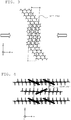
- Figure 3 is a schematic diagram schematically showing the view of the crystal structure of the organic semiconductor layer 30, as viewed from the b-axis direction
- Figure 4 is a schematic diagram schematically showing the view of the crystal structure of the organic semiconductor layer 30, as viewed from the a-axis direction
- Figure 5 is an explanatory diagram showing a relation between carrier mobility and magnitude of a strain in the organic semiconductor layer 30.
- the three crystal axes (the a-axis, the b-axis and the c-axis) are shown by arrows, and a unit cell is surrounded by a quadrangle.
- the carrier mobility changes depending on the magnitude of the given strain, as shown in Figure 5 .
- the carrier mobility is determined depending on the magnitude of the strain to be given, and increases as the strain to be given increases. For example, the carrier mobility when the strain is 3% is 16.5 [cm 2 /(V ⁇ s)], which is 1.7 times the carrier mobility when the strain is 0%.
- multi-crystal organic semiconductors differ in crystal structure, depending on the formation technique.
- FIG. 6 is a schematic diagram schematically showing how molecules vibrate before and after a compressive stress is applied to the single-crystal organic semiconductor.
- the single-crystal organic semiconductor has a property of increasing the carrier mobility as the strain to be given increases, and this property is consistent regardless of the formation technique for the organic semiconductor.
- the organic semiconductor layer 30 since the organic semiconductor layer 30 is formed as the single-crystal thin film, the organic semiconductor layer 30 can have uniform property with respect to the strain (the property of increasing the carrier mobility as the strain to be given increases).
- the magnitude of the strain of an object is detected, in the following procedure.
- a predetermined voltage is applied to the gauge leads 32 in a state where the substrate 22 sticks with the object to be detected.
- the strain of the object to be detected changes, the stress to be applied to the organic semiconductor layer 30 together with the substrate 22 changes, and the strain to be given to the organic semiconductor layer 30 changes.
- the strain to be given to the organic semiconductor layer 30 changes, the carrier mobility in the organic semiconductor layer 30 changes depending on the magnitude of the strain, and the gauge current to flow through the gauge leads 32 changes.
- the organic semiconductor element 20 by measuring the change in the gauge current, it is possible to measure the magnitude of the strain of the object to be detected.
- the organic semiconductor layer 30, which is formed as the single-crystal thin film has uniform property with respect to the strain, and therefore, it is possible to provide strain sensors having uniform property.
- the organic semiconductor layer 30 is formed as the single-crystal thin film, it is possible to measure the magnitude of the strain of the detection target. Further, since the organic semiconductor layer 30 is formed as the single-crystal thin film, it is possible to obtain the same carrier mobility when the same strain is given, and it is possible to provide strain sensors having uniform property.
- the organic semiconductor element 20 functions as a strain sensor.
- the organic semiconductor element 20 is not limited to elements that function as a strain sensor in this way, and may be used as any element that operates based on the carrier mobility when the strain changes (the carrier mobility when a predetermined strain as the standard is given and the carrier mobility when a different strain from the predetermined strain is given), as exemplified by a pressure sensor that detects the pressure given to a pressure sensitive part, and a temperature sensor that detects temperature.
- the organic semiconductor element may be stuck to a sheet, and based on the current (the carrier mobility) that flows when the strain of the organic semiconductor element changes by the press of the sheet, the pressure given to the sheet may be detected.
- the organic semiconductor element may be bonded to metals having different thermal expansion coefficients similarly to a bi-metal, and based on the current (the carrier mobility) when the strain of the organic semiconductor element changes due to the difference in thermal expansion coefficient caused by the change in temperature, the temperature may be detected.
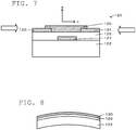
- FIG. 7 is an explanatory diagram showing an exemplary configuration of the organic semiconductor element 120 according to the second embodiment of the present invention.
- the organic semiconductor element 120 which is configured as a top contact-bottom gate type field-effect transistor, includes a substrate 122, a gate electrode 124 formed on a predetermined region of the substrate 122, a gate insulating film 126 formed on the substrate 122 and the gate electrode 124, an organic semiconductor layer 130 formed on the gate insulating film 126 so as to be positioned above the gate electrode 124, and a source electrode 132 and drain electrode 134 formed on the gate insulating film so as to be positioned on both sides of the organic semiconductor layer 130.
- the substrate 122 is formed of a plastic (for example, polyethylene naphthalate), such that the thickness is 50 ⁇ m to 10 mm, for example, 100 ⁇ m to 200 ⁇ m.
- a plastic for example, polyethylene naphthalate
- the gate electrode 124, the source electrode 132 and the drain electrode 134 are formed of a metal material such as gold.
- the gate electrode 124 is formed such that the thickness is 50 nm or less, for example, 40 nm or 30 nm.
- the source electrode 132 and the drain electrode 134 are formed such that the thickness is 50 nm or less, for example, 40 nm or 30 nm.
- the gate insulating film 126 is formed of an insulating material (for example, polymethyl methacrylate), such that the thickness is 200 nm or less, for example, 150 nm or 100 nm.
- an insulating material for example, polymethyl methacrylate
- the organic semiconductor layer 130 is formed such that the thickness is 200 nm or less, for example, 100 nm or 50 nm, as a single-crystal thin film of an organic semiconductor having the above-described structure shown in Formula (1).
- the organic semiconductor layer 130 is formed such that the c-axis of the crystal axes in the crystal structure shown in Figure 3 is parallel to the orientation of a channel to be formed, and is kept in a state where a predetermined strain is applied by applying a compressive stress in the c-axis direction.
- the "predetermined strain” only needs to be a strain by which the organic semiconductor layer 130, the substrate 122 or the gate insulating film 126 is not broken, and in the embodiment, a strain of 10% or less in the compression direction, for example, a strain of 3% in the compression direction can be used.
- FIG. 8 is an explanatory diagram showing an exemplary formation method for the organic semiconductor layer 130.
- a single-crystal thin film of the organic semiconductor (the organic semiconductor layer 30) is formed in the right-left direction in the figure, in a state where the substrate 122 having the gate insulating film 126 formed is bent. Thereafter, the substrate 122 is stretched until the substrate 122 becomes planar, and the compressive stress is applied to the thin film. Thereby, the organic semiconductor layer 130 kept in the state where the predetermined strain is applied is formed.
- the method for keeping the organic semiconductor layer 130 in a state where a predetermined strain is applied other than the method exemplified in Figure 8 , it is allowable to use another method such as a method of forming a single-crystal thin film of the organic semiconductor in a state where the substrate 122 is heated and is thermally expanded and thereafter thermally contracting the substrate 122 at normal temperature.
- the organic semiconductor layer 130 is formed as the single-crystal thin film in this way, it is possible to obtain the same carrier mobility when the same compressive stress is applied to and the same strain is given to the organic semiconductor layer 130. Accordingly, the organic semiconductor layer 130 can have uniform property with respect to the strain.
- the organic semiconductor element 120 configured in this way operates as a transistor, when a channel is formed in the organic semiconductor layer 130 by applying voltages for operation to the gate electrode 124, the source electrode 132 and the drain electrode 134 respectively.
- the organic semiconductor layer 130 which is formed as the single-crystal thin film, has uniform property with respect to the strain, and therefore, it is possible to provide transistors having uniform property. Further, since the organic semiconductor layer 130 is kept in the state where the strain is applied, the carrier mobility is higher compared to when the strain is not applied. Therefore, it is possible to make a larger current flow between the source electrode 132 and the drain electrode 134, and it is possible to provide a transistor having a higher drive power.
- the organic semiconductor layer 130 is formed as the single-crystal thin film, it is possible to provide a transistor having a high drive power. Further, since the organic semiconductor layer 130 is formed as the single-crystal thin film, it is possible to obtain the same carrier mobility when the same strain is given, and it is possible to provide transistors having uniform property.
- the organic semiconductor element 120 is configured as a top contact-bottom gate type field-effect transistor, but may be configured as any type of transistor that can be formed on an inorganic semiconductor such as silicon and gallium nitride, as exemplified by a top contact-top gate type field-effect transistor. Further, the organic semiconductor element is not limited to such transistor, and may be used as any element that can be kept in a state where a predetermined strain is applied in the movement direction of the carrier.
- the organic semiconductor layers 30, 130 are formed of the organic semiconductor having the above-described structure in Formula (1).
- the organic semiconductor for example, a polycyclic aromatic compound with four or more rings or a polycyclic compound with four or more rings including one or a plurality of unsaturated five-membered heterocyclic compounds and a plurality of benzene rings can be used.
- any structure in the following Formula (2) to Formula (14) may be adopted.
- R a straight alkyl, a branched alkyl, a fluorinated straight/branched alkyl, triisopropylsilylethynyl, phenyl or the like can be used.
- the present invention can be utilized in production industries for an organic semiconductor element, and the like.
Landscapes
- Physics & Mathematics (AREA)
- Engineering & Computer Science (AREA)
- Chemical & Material Sciences (AREA)
- Materials Engineering (AREA)
- Spectroscopy & Molecular Physics (AREA)
- General Physics & Mathematics (AREA)
- Manufacturing & Machinery (AREA)
- Composite Materials (AREA)
- Thin Film Transistor (AREA)
- Electroluminescent Light Sources (AREA)
- Pressure Sensors (AREA)
Applications Claiming Priority (2)
| Application Number | Priority Date | Filing Date | Title |
|---|---|---|---|
| JP2015015744A JP6116018B2 (ja) | 2015-01-29 | 2015-01-29 | 有機半導体素子 |
| PCT/JP2016/052266 WO2016121791A1 (ja) | 2015-01-29 | 2016-01-27 | 有機半導体素子 |
Publications (2)
| Publication Number | Publication Date |
|---|---|
| EP3252829A1 true EP3252829A1 (de) | 2017-12-06 |
| EP3252829A4 EP3252829A4 (de) | 2018-09-26 |
Family
ID=56543402
Family Applications (1)
| Application Number | Title | Priority Date | Filing Date |
|---|---|---|---|
| EP16743394.5A Pending EP3252829A4 (de) | 2015-01-29 | 2016-01-27 | Organisches halbleiterelement |
Country Status (5)
| Country | Link |
|---|---|
| US (2) | US10854825B2 (de) |
| EP (1) | EP3252829A4 (de) |
| JP (1) | JP6116018B2 (de) |
| CN (2) | CN113285023A (de) |
| WO (1) | WO2016121791A1 (de) |
Cited By (1)
| Publication number | Priority date | Publication date | Assignee | Title |
|---|---|---|---|---|
| CN112997332A (zh) * | 2018-09-04 | 2021-06-18 | 国立大学法人东京大学 | 有机半导体元件、应变传感器、振动传感器以及有机半导体元件的制造方法 |
Families Citing this family (5)
| Publication number | Priority date | Publication date | Assignee | Title |
|---|---|---|---|---|
| EP3930018A4 (de) * | 2019-02-22 | 2022-11-09 | The University of Tokyo | Organisches halbleiterbauelement, verfahren zur herstellung einer organischen halbleiter-einkristallschicht und verfahren zur herstellung eines organischen halbleiterbauelements |
| CN110487455A (zh) * | 2019-08-07 | 2019-11-22 | 北京理工大学 | 一种光辅助提高应力传感器灵敏度的方法 |
| JP7493228B2 (ja) * | 2019-09-03 | 2024-05-31 | 国立研究開発法人産業技術総合研究所 | 有機半導体材料および有機薄膜トランジスタ |
| CN115362346A (zh) * | 2020-03-19 | 2022-11-18 | 深圳纽迪瑞科技开发有限公司 | 一种应变感测膜、压力传感器、混合应变感测系统 |
| EP4492024A4 (de) | 2022-08-22 | 2026-03-18 | Univ Tokyo | Organisches halbleiterelement, dehnungsmesser, messvorrichtung und herstellungsverfahren für ein organisches halbleiterelement |
Family Cites Families (21)
| Publication number | Priority date | Publication date | Assignee | Title |
|---|---|---|---|---|
| KR20050028020A (ko) * | 2002-07-15 | 2005-03-21 | 파이오니아 가부시키가이샤 | 유기 반도체 소자 및 그 제조 방법 |
| JP2005079204A (ja) * | 2003-08-28 | 2005-03-24 | Canon Inc | 電界効果型トランジスタおよびその製造方法 |
| JP4736318B2 (ja) | 2003-11-28 | 2011-07-27 | Tdk株式会社 | 積層体の製造方法及び有機電界効果トランジスタの製造方法 |
| US20050211973A1 (en) * | 2004-03-23 | 2005-09-29 | Kiyotaka Mori | Stressed organic semiconductor |
| WO2006046521A1 (ja) | 2004-10-25 | 2006-05-04 | Matsushita Electric Industrial Co., Ltd. | 電子デバイスおよびその製造方法、ならびにそれを用いた電子機器 |
| US7671448B2 (en) * | 2005-03-24 | 2010-03-02 | Semiconductor Energy Laboratory Co., Ltd. | Semiconductor device including two organic semiconductor layers |
| CN101253610A (zh) * | 2005-08-31 | 2008-08-27 | 住友化学株式会社 | 晶体管、有机半导体元件及它们的制造方法 |
| JP4316669B2 (ja) | 2006-06-07 | 2009-08-19 | パナソニック株式会社 | 半導体素子の製造方法および電子デバイスの製造方法 |
| EP2232606A1 (de) * | 2007-12-17 | 2010-09-29 | 3M Innovative Properties Company | Lösungsverarbeitbare organische halbleiter auf der basis von anthracen |
| JP5478189B2 (ja) | 2009-10-16 | 2014-04-23 | 学校法人東海大学 | 大気安定性に優れた有機トランジスタ |
| JP5666474B2 (ja) * | 2009-12-14 | 2015-02-12 | 出光興産株式会社 | 多環縮環化合物、及び、それを用いた有機薄膜トランジスタ |
| JP2011242153A (ja) * | 2010-05-14 | 2011-12-01 | Citizen Holdings Co Ltd | 歪センサおよび歪み測定方法 |
| JPWO2012165612A1 (ja) | 2011-06-03 | 2015-02-23 | 国立大学法人九州大学 | 有機半導体材料及び有機エレクトロニクスデバイス |
| JP5950251B2 (ja) * | 2011-09-09 | 2016-07-13 | 国立研究開発法人物質・材料研究機構 | 有機半導体単結晶形成方法 |
| JPWO2013065582A1 (ja) | 2011-11-04 | 2015-04-02 | ソニー株式会社 | 有機半導体素子の製造方法、有機半導体素子、有機単結晶薄膜の成長方法、有機単結晶薄膜、電子機器および有機単結晶薄膜群 |
| JP2013159584A (ja) * | 2012-02-07 | 2013-08-19 | Univ Of Tokyo | 電子材料およびこれを用いた電子素子 |
| JP2014049722A (ja) * | 2012-09-04 | 2014-03-17 | Nec Corp | 有機半導体トランジスタおよびその製造方法 |
| CN105102462B (zh) * | 2013-03-05 | 2018-02-02 | 捷恩智株式会社 | 含有氧族元素的有机化合物、其制造方法以及用途 |
| KR102196923B1 (ko) * | 2013-04-25 | 2020-12-31 | 파이 크리스탈 가부시키가이샤 | 유기 반도체 박막의 제조 방법 |
| WO2015137304A1 (ja) | 2014-03-12 | 2015-09-17 | Dic株式会社 | 化合物、並びにそれを含有する有機半導体材料、有機半導体インク及び有機トランジスタ |
| JP6590361B2 (ja) | 2014-03-20 | 2019-10-16 | パイクリスタル株式会社 | 有機半導体膜及びその製造方法 |
-
2015
- 2015-01-29 JP JP2015015744A patent/JP6116018B2/ja active Active
-
2016
- 2016-01-27 CN CN202110544249.9A patent/CN113285023A/zh active Pending
- 2016-01-27 CN CN201680018138.1A patent/CN107431095B/zh active Active
- 2016-01-27 US US15/547,594 patent/US10854825B2/en active Active
- 2016-01-27 WO PCT/JP2016/052266 patent/WO2016121791A1/ja not_active Ceased
- 2016-01-27 EP EP16743394.5A patent/EP3252829A4/de active Pending
-
2019
- 2019-07-03 US US16/502,174 patent/US10903434B2/en active Active
Cited By (3)
| Publication number | Priority date | Publication date | Assignee | Title |
|---|---|---|---|---|
| CN112997332A (zh) * | 2018-09-04 | 2021-06-18 | 国立大学法人东京大学 | 有机半导体元件、应变传感器、振动传感器以及有机半导体元件的制造方法 |
| EP3848987A4 (de) * | 2018-09-04 | 2022-05-25 | The University of Tokyo | Organisches halbleiterelement, dehnungssensor, schwingungssensor und herstellungsverfahren für ein organisches halbleiterelement |
| US12068093B2 (en) | 2018-09-04 | 2024-08-20 | The University Of Tokyo | Organic semiconductor element, strain sensor, vibration sensor, and manufacturing method for organic semiconductor element |
Also Published As
| Publication number | Publication date |
|---|---|
| JP6116018B2 (ja) | 2017-04-19 |
| US20180145266A1 (en) | 2018-05-24 |
| US10903434B2 (en) | 2021-01-26 |
| CN113285023A (zh) | 2021-08-20 |
| JP2016143675A (ja) | 2016-08-08 |
| CN107431095A (zh) | 2017-12-01 |
| US20190326522A1 (en) | 2019-10-24 |
| WO2016121791A1 (ja) | 2016-08-04 |
| CN107431095B (zh) | 2021-06-01 |
| EP3252829A4 (de) | 2018-09-26 |
| US10854825B2 (en) | 2020-12-01 |
Similar Documents
| Publication | Publication Date | Title |
|---|---|---|
| US10903434B2 (en) | Organic semiconductor element | |
| US10504756B2 (en) | Wafer processing method and apparatus | |
| Munzenrieder et al. | Design rules for IGZO logic gates on plastic foil enabling operation at bending radii of 3.5 mm | |
| Li et al. | Oxide semiconductor thin film transistors on thin solution-cast flexible substrates | |
| KR20140032093A (ko) | 압력 센서 및 압력 센싱 방법 | |
| Richter et al. | Piezoresistance of silicon and strained Si0. 9Ge0. 1 | |
| Nguyen et al. | High-temperature tolerance of the piezoresistive effect in p-4H-SiC for harsh environment sensing | |
| CN102832177A (zh) | 用于从基部基底受控地移除半导体器件层的方法 | |
| US9666493B2 (en) | Semiconductor device structure with 110-PFET and 111-NFET curent flow direction | |
| Niu et al. | Epitaxial systems combining oxides and semiconductors | |
| US9972723B2 (en) | Piezoelectric thin-film based flexible sensing device, method for fabrication thereof and method for operating the same | |
| Ling et al. | Non-destructive probing of the anisotropy of field-effect mobility in the rubrene single crystal | |
| KR101611811B1 (ko) | 연성 기판들 상에 전자 디바이스들을 제조하기 위한 버퍼 층의 어닐링 | |
| EP2653844A1 (de) | Integrierter piezoelektrischer Sensor zur statischen Druckmessung | |
| JP6635466B2 (ja) | 有機半導体素子 | |
| EP2690418A1 (de) | Drucksensor mit flexibler Membran mit aktiven Schaltungskomponenten darauf | |
| EP2573803A4 (de) | Siliciumnitridfilm für ein halbleiterbauelement sowie verfahren und vorrichtung zur herstellung des siliciumnitridfilms | |
| WO2015038131A3 (en) | Variable ice and methods for measuring sample properties with the same | |
| US20090294853A1 (en) | Thin film transistor having a common channel and selectable doping configuration | |
| US10840377B2 (en) | Flexible high performance inorganic matter FET using built-in strain of inorganic matter on insulator wafer | |
| Seok et al. | A study on effect of wafer bow in wafer-level BCB cap transfer packaging | |
| Ghoneim et al. | Ultra-high density out-of-plane strain sensor 3D architecture based on sub-20 nm PMOS FinFET | |
| Balbola et al. | Experimental characterization of the influence of transverse prestrain on the piezoresistive coefficients of heavily doped n-type silicon | |
| Zumeit et al. | Si Nanoribbons based High Performance Printed FETs using Room-Temperature deposited Dielectric | |
| Reyes-Martinez | Mechanical and Electro-Mechanical Properties of Crystalline Organic Semiconductors |
Legal Events
| Date | Code | Title | Description |
|---|---|---|---|
| STAA | Information on the status of an ep patent application or granted ep patent |
Free format text: STATUS: THE INTERNATIONAL PUBLICATION HAS BEEN MADE |
|
| PUAI | Public reference made under article 153(3) epc to a published international application that has entered the european phase |
Free format text: ORIGINAL CODE: 0009012 |
|
| STAA | Information on the status of an ep patent application or granted ep patent |
Free format text: STATUS: REQUEST FOR EXAMINATION WAS MADE |
|
| 17P | Request for examination filed |
Effective date: 20170828 |
|
| AK | Designated contracting states |
Kind code of ref document: A1 Designated state(s): AL AT BE BG CH CY CZ DE DK EE ES FI FR GB GR HR HU IE IS IT LI LT LU LV MC MK MT NL NO PL PT RO RS SE SI SK SM TR |
|
| AX | Request for extension of the european patent |
Extension state: BA ME |
|
| DAV | Request for validation of the european patent (deleted) | ||
| DAX | Request for extension of the european patent (deleted) | ||
| A4 | Supplementary search report drawn up and despatched |
Effective date: 20180823 |
|
| RIC1 | Information provided on ipc code assigned before grant |
Ipc: H01L 21/336 20060101ALI20180817BHEP Ipc: H01L 29/84 20060101ALI20180817BHEP Ipc: H01L 29/786 20060101AFI20180817BHEP Ipc: H01L 51/05 20060101ALI20180817BHEP Ipc: G01L 1/18 20060101ALI20180817BHEP |
|
| STAA | Information on the status of an ep patent application or granted ep patent |
Free format text: STATUS: EXAMINATION IS IN PROGRESS |
|
| 17Q | First examination report despatched |
Effective date: 20200709 |
|
| RIC1 | Information provided on ipc code assigned before grant |
Ipc: H01L 21/336 19900101ALI20230112BHEP Ipc: H01L 29/786 19950101AFI20230112BHEP |
|
| GRAP | Despatch of communication of intention to grant a patent |
Free format text: ORIGINAL CODE: EPIDOSNIGR1 |
|
| STAA | Information on the status of an ep patent application or granted ep patent |
Free format text: STATUS: GRANT OF PATENT IS INTENDED |
|
| INTG | Intention to grant announced |
Effective date: 20240528 |
|
| GRAJ | Information related to disapproval of communication of intention to grant by the applicant or resumption of examination proceedings by the epo deleted |
Free format text: ORIGINAL CODE: EPIDOSDIGR1 |
|
| STAA | Information on the status of an ep patent application or granted ep patent |
Free format text: STATUS: EXAMINATION IS IN PROGRESS |
|
| INTC | Intention to grant announced (deleted) | ||
| REG | Reference to a national code |
Ref country code: DE Ref legal event code: R079 Free format text: PREVIOUS MAIN CLASS: H01L0029786000 Ipc: H10K0077000000 |
|
| GRAP | Despatch of communication of intention to grant a patent |
Free format text: ORIGINAL CODE: EPIDOSNIGR1 |
|
| STAA | Information on the status of an ep patent application or granted ep patent |
Free format text: STATUS: GRANT OF PATENT IS INTENDED |
|
| RIC1 | Information provided on ipc code assigned before grant |
Ipc: H10K 77/00 20230101AFI20260326BHEP |