EP3254862B3 - Élément de marquage de produits - Google Patents
Élément de marquage de produits Download PDFInfo
- Publication number
- EP3254862B3 EP3254862B3 EP17174013.7A EP17174013A EP3254862B3 EP 3254862 B3 EP3254862 B3 EP 3254862B3 EP 17174013 A EP17174013 A EP 17174013A EP 3254862 B3 EP3254862 B3 EP 3254862B3
- Authority
- EP
- European Patent Office
- Prior art keywords
- pixels
- electromagnetic radiation
- diffraction
- radiation
- labelling element
- Prior art date
- Legal status (The legal status is an assumption and is not a legal conclusion. Google has not performed a legal analysis and makes no representation as to the accuracy of the status listed.)
- Active
Links
Images





Classifications
-
- B—PERFORMING OPERATIONS; TRANSPORTING
- B42—BOOKBINDING; ALBUMS; FILES; SPECIAL PRINTED MATTER
- B42D—BOOKS; BOOK COVERS; LOOSE LEAVES; PRINTED MATTER CHARACTERISED BY IDENTIFICATION OR SECURITY FEATURES; PRINTED MATTER OF SPECIAL FORMAT OR STYLE NOT OTHERWISE PROVIDED FOR; DEVICES FOR USE THEREWITH AND NOT OTHERWISE PROVIDED FOR; MOVABLE-STRIP WRITING OR READING APPARATUS
- B42D25/00—Information-bearing cards or sheet-like structures characterised by identification or security features; Manufacture thereof
- B42D25/30—Identification or security features, e.g. for preventing forgery
- B42D25/328—Diffraction gratings; Holograms
Definitions
- the invention relates to a method for identifying products.
- Hologram labels tracer technologies based on RFID or generative methods such as e.g. the use of fluorescent nanoparticles.
- Especially on established hologram labels come highly complex security elements, such as Identigrams, kinegrams, computer generated holograms or nanograms are used. This provides visual, sensory or microcoscopic options for identification.
- Computer-generated holograms are usually generated with the aid of micro- and nanostructures, which generate defined wave fronts and can therefore provide a complex diffraction pattern as a security feature.
- the production of the micro- and nanostructures is usually only possible with complex, cost-intensive and complicated methods, such as electron beam lithography.
- complex algorithms such as the iterative Fourier transformation algorithm, are used.
- complex, diffractive security elements can be used by means of selective surface structuring, which can be implemented both directly and indirectly.
- pixograms can be used by means of selective surface structuring, which can be implemented both directly and indirectly.
- the effort for the production of the complex, diffractive security elements is significantly lower, both from a financial and a time perspective.
- a visual inspection of diffractive security elements is usually carried out by irradiation with monochromatic, electromagnetic radiation.
- a plurality of pixels each with a periodic lattice structure, in particular a linear lattice structure, are formed on one surface.
- Grid structures with a structure period mit and an alignment of the linear structure elements aligned parallel to one another with an angle ⁇ with respect to a reference axis are formed in individual pixels in such a way that when the pixels forming the identification element are irradiated with electromagnetic radiation on a detector array or a surface, an image is formed of the identification element by images of at least one order of the electromagnetic radiation diffracted by pixels. The image can then be used to identify the respective labeling element.
- the position of the electromagnetic radiation diffracted and transmitted or reflected by the respective pixel can be influenced in a defined manner in at least one diffraction order by the respective choice of the structure period ⁇ and / or the choice of the angle ⁇ .
- the structuring of the individual pixels of a labeling element can be selected such that the pattern of the pixels formed on the surface of a product does not correspond to the two-dimensional structure or the structure of the labeling element. When viewed directly, it cannot be recognized as the respective labeling element. Only after the diffraction of the electromagnetic radiation on the lattice-shaped structure can the actual image of the identification element with the images of the diffraction orders of the pixels be recognized as such.
- Monochromatic radiation should be used for the radiation, which is preferably emitted by a laser diode onto the surface structured with pixels.
- the illustration can be for products made of optically transparent Materials in the radiation direction behind the product, but also with electromagnetic radiation reflected from the surface and diffracted at the structural elements.
- Pixels can also be present, each of which additionally has a different structure depth of the linear structure elements.
- images can be achieved which are locally defined and have different intensities associated with the correspondingly configured structural elements, which can bring about a further possibility for differentiating usable identification elements and increasing the security against forgery.
- the pixels of a labeling element can and should be designed such that the labeling element as such cannot be recognized on the surface of the product without optical aids.
- the pixels in particular should not be easily recognizable. It should therefore not be visually perceptible without the use of magnifying optical elements, in particular optical lenses.
- the pixels can be circular or polygonal. For example, they can be arranged in a row and column arrangement, in which different numbers of pixels can be formed in individual rows and columns.
- the individually structured pixels should each occupy a maximum area of 1 mm 2 .
- the structured total area (ie the sum of all individual pixels) can be of any size.
- the pixels should have a structure period ⁇ in the range of 0.01 ⁇ m - 50 ⁇ m and / or structure depths in the range of 0.001 ⁇ m - 10 ⁇ m.
- At least electromagnetic radiation of a diffraction order preferably of the 1st order
- a combination of different diffraction orders is also possible.
- at least one radiation source, a detector array and / or a display for displaying the image of the pixels form a unit with the respective diffraction order.
- a radiation source can be arranged on a surface, with which electromagnetic radiation is directed onto the surface provided with lattice-shaped structures. Electromagnetic radiation reflected and diffracted from there can then strike a detector array arranged on the same side and be converted there into electrical signals in a spatially resolved manner.
- An optical display element can be present on the rear surface, with which the detected electrical signals enable an identification element to be imaged, which can be recognized by a user and compared with a specification.
- a pattern recognition can also be integrated, with which a check for authenticity can be reached electronically. The test result can then be displayed visually or acoustically.
- wavelength-optimized, structured areas of a marking element can direct electromagnetic radiation onto wavelength-optimized, structured areas of a marking element, so that in combination wavelength-selective security features can be evaluated and taken into account during a check.
- the surface structuring of the individual pixels which is designed in the form of an optical grating, is carried out by means of direct laser interference structuring (DLIP) known per se in a simple, inexpensive and flexible manner.
- DLIP direct laser interference structuring
- Embossing tools that are produced, for example, by replicating structural elements formed with DLIP can also be used.
- complex security features can be made available as identification elements because of the complex diffraction patterns that can be achieved.
- a check for the authenticity of a product, for example, can be carried out almost anywhere using very simple optical means. Mobile devices can be used for this.
- a marking element can be formed directly on a surface of a product, but also on an element that can be connected to the respective product.
- the pixels forming the identification element in at least one surface of a material which is covered by at least one other material or is formed within an interface between the materials.
- the other material should have a smaller absorption capacity, in particular an absorption capacity for the laser radiation used to form the pixels, which absorption capacity is at least 50% smaller than the material covered with the other material.
- the other material should very particularly preferably not absorb the wavelength of the laser radiation used.
- Sublimation that is to say transfer of, in particular, polymeric material
- polymeric material is at least partially converted into the gas phase.
- Gas can then remain between the two materials and achieve the desired effect.
- Melting or remelting can also be achieved in a locally defined manner.
- a suitable focusing of the partial beams used on the surface of the material covered by another material or an interface formed by one and another material can be selected in the corresponding plane in order to be able to form very fine, filigree structures of a marking element.
- the at least one other material should be a polymer, in particular a polymer film.
- the materials should be cohesive, preferably connected with an organic binder.
- a part can be formed from a material that is covered by two different materials on two oppositely arranged surfaces.
- the other materials can be the same but also different.
- PMMA polymethyl methacrylate
- PC polycarbonate
- PP polypropylene
- PET polyethylene
- PMMA and PI polyimide
- PMMA and PEEK polyether ether ketone
- PET and PI are processed accordingly at a wavelength of 355 nm.
- the first-mentioned polymer is the other material that covers a material.
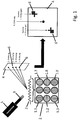
- FIG. 1 An example of a labeling element 2 with nine pixels 1.1 to 1.9 is shown in a top view and a side view.
- the pixels 1.1 to 1.9 were each formed as a structured, circular surface with a linear grid structure using DLIP.
- the top view shows that the alignment of the lattice structures has been selected at different angles / orientations.
- FIG. 1 Above the in Figure 1 top view shown is a corresponding structured surface of a product shown.
- Monochromatic electromagnetic radiation 3 from a laser diode as radiation source 5 is directed onto this structured surface.
- the electromagnetic radiation which is refracted and reflected on the structured surface of the pixels 1.1 to 1.9 forming the marking element 2 impinges on a detector array 4 with which the intensities are detected in a spatially resolved manner.
- Figure 6 can be detected in several diffraction orders. For a check, however, it may be sufficient to consider only one diffraction order, preferably the 1st order.
- pixels 1.1 to 1.9 can look at the detector array 4. After reflection and refraction, pixels 1.1 to 1.9 are mapped by the respective selection of the structure period ⁇ and the angle ⁇ for the alignment of the linear lattice structure of the individual pixels and at least one Figure 6 of the entire labeling element 2 in the 1st diffraction order can be used for a test for authenticity.
- This illustration shows two images 6 of the first diffraction order of the labeling element.
- the illustration (s) 6 correspond to the respectively given identification element 2.
- the radiation with electromagnetic radiation 3 can take place at different angles. Depending on the selected angle, only the position of the entire one changes Figure 6 .
- Grid structure is aligned with respect to an axis of a coordinate system, has an influence on the position of the image of a pixel 1 after the diffraction of electromagnetic radiation on the linear grid structure.
- the angle ⁇ 1 has a value of 90 ° in relation to an x-axis of a coordinate system and the angle ⁇ 2 has a value of 135 ° in relation to the x-axis of a coordinate system.
- the images of the diffraction orders of a pixel 1 with the structure period ⁇ 1 and an angle ⁇ 2 are not arranged on an axis on which the corresponding images of diffraction orders with structure periods ⁇ 1 and ⁇ 2 and the angle ⁇ 1 lie.
- the respective positions of images of pixels after the optical diffraction can thus be influenced by a suitable choice of the structure period ⁇ and / or the angle ⁇ of the individual pixels 1.
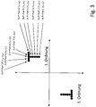
- FIG 3 a coordinate system is shown in which a Figure 6 the 1st diffraction order of 10 pixels led to a T-shaped identification element 2.
- Different values for the structure period ⁇ and angle ⁇ have been selected on the individual images of pixels, so that each diffraction is shown corresponding to the respective identification element after the diffraction at the desired position and in this example the identification element 2 has the shape of a "T"" Has.
- the respective choice of the structure period ⁇ and the angle ⁇ of the respective linear grid structure can also be made available with differently designed identification elements 2.
- the structure period ⁇ can be varied in the range 1.2 ⁇ m to 1.6 ⁇ m, the angle ⁇ in the range 24 ° to 52 ° for individual pixels.
- the structure depth of linear lattice structures can be kept constant in the range of 0.001 ⁇ m to 10 ⁇ m and also for all pixels that are assigned to a marking element 2
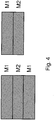
- FIG 4 an arrangement is shown on the left in which a material M2 of another material M1 is covered.
- the illustration on the right shows an arrangement in which a material M2 is covered by another material M1 on two opposite surfaces.
- a material can also be covered on two opposite surfaces by other materials and the other materials are different.
- the materials M1 and M2 are arranged directly one above the other without gaps. However, an arrangement at a distance from one another is also possible.
- the materials can be fixed on the outside with a frame.
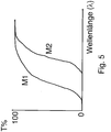
- FIG. 5 The diagram shown shows the differences in the wavelength-dependent transparency for electromagnetic radiation for different materials M1 and M2.
- a wavelength that is identified by the dashed line can therefore preferably be used to form a marking element in a material M2.
- FIGS. 6a and 6b illustrate how structural elements can be formed in the surface of a material M2 by means of DLIP with individual pixels 1.1 to 1.3, in that several partial beams 9 and 9 'can simultaneously be directed locally defined onto the surface of a material M2 by another material M1 covering it.
- Material M1 absorbs at least 80%, preferably almost 100%, of the electromagnetic laser radiation at the selected wavelength ⁇ , whereas the other material M1 does not absorb the electromagnetic radiation with the corresponding wavelength at all, or at most 40%.
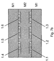
- Figures 7a and 7b shows how pixels 1.1 to 1.6 were formed to form a marking element on two oppositely arranged surfaces of a material M2. In this case, they form an almost identical pattern because they have been formed mirrored to the center axis of the material M2. However, an offset arrangement of pixels 1.1 to 1.3, 1.4 to 1.6 and 1.7 to 1.9 is also possible. This is with the representations in Figure 9 (symmetrically on the left on a surface of a material M2 and on the right offset to one another in rows on a surface or one above the other on two surfaces of a material M2).
- Figure 8 it can be seen that individual pixels 1.1 to 1.3 structure elements 10 with a lateral dimension D in an axial direction with 2 ⁇ m to 20 mm with a distance A from one another of 0 nm to 20,000 ⁇ m, preferably from 100 nm to 50 ⁇ m, can be sensibly formed. Individual pixels can be formed with a dimensioning ⁇ in the range from 100 nm to 50 ⁇ m.
Landscapes
- Credit Cards Or The Like (AREA)
- Diffracting Gratings Or Hologram Optical Elements (AREA)
Claims (5)
- Procédé d'identification pour des produits possédant un élément d'identification, dans lequel, sur une surface, plusieurs pixels (1.1 à 1.x) avec des structures de grilles périodiques, plus particulièrement des structures de grilles linéaires, sont prévus en tant qu'élément d'identification en utilisant la structuration de l'interférence laser directe et, dans certains pixels (1.1 à 1.x), sont réalisées des structures de grilles avec chacune une période de structure Λ et une orientation des éléments de structure linéaires, orientés plus particulièrement de manière parallèle entre eux, formant un angle ϕ par rapport à un axe de référence, de sorte que, lors d'une irradiation des pixels (1.1 à 1.x) constituant l'élément d'identification (2) avec un rayonnement électromagnétique (3), de préférence un rayonnement électromagnétique monochromatique provenant d'au moins une source de rayonnement, des représentations d'au moins un ordre de diffraction du rayonnement électromagnétique (3) diffracté par les pixels (1.1 à 1.x) sont obtenues, et
les représentations de l'élément d'identification (2) de l'au moins un ordre de diffraction ont lieu sur une matrice de détecteur (4) et celui-ci peut être utilisé pour l'identification de l'élément d'identification (2) correspondant. - Procédé selon la revendication 1, caractérisé en ce que plusieurs sources de rayonnement de différentes longueurs d'ondes sont utilisées pour l'irradiation.
- Procédé selon la revendication 1 ou 2, caractérisé en ce que des rayonnements électromagnétiques de plusieurs longueurs d'ondes sont orientés vers des zones structurées de manière optimisée pour des longueurs d'ondes, de façon à ce que des caractéristiques de sécurité sélectives pour des longueurs d'ondes soient analysées.
- Procédé selon l'une des revendications précédentes, caractérisé en ce que, avec un élément d'affichage optique, une représentation d'un élément d'identification (2) reconnaissable par l'utilisateur est obtenue et est comparée avec une référence.
- Procédé selon l'une des revendications précédentes, caractérisé en ce que, avec une détection de motif, un contrôle en temps réel a lieu, de préférence le résultat du contrôle de la détection de motif étant affiché de manière visuelle ou optique.
Applications Claiming Priority (2)
| Application Number | Priority Date | Filing Date | Title |
|---|---|---|---|
| DE102016210119 | 2016-06-08 | ||
| DE102016215160.6A DE102016215160A1 (de) | 2016-06-08 | 2016-08-15 | Kennzeichnungselement für Produkte |
Publications (3)
| Publication Number | Publication Date |
|---|---|
| EP3254862A1 EP3254862A1 (fr) | 2017-12-13 |
| EP3254862B1 EP3254862B1 (fr) | 2019-02-27 |
| EP3254862B3 true EP3254862B3 (fr) | 2020-04-29 |
Family
ID=59053914
Family Applications (1)
| Application Number | Title | Priority Date | Filing Date |
|---|---|---|---|
| EP17174013.7A Active EP3254862B3 (fr) | 2016-06-08 | 2017-06-01 | Élément de marquage de produits |
Country Status (1)
| Country | Link |
|---|---|
| EP (1) | EP3254862B3 (fr) |
Family Cites Families (3)
| Publication number | Priority date | Publication date | Assignee | Title |
|---|---|---|---|---|
| DE102011014114B3 (de) * | 2011-03-15 | 2012-05-10 | Ovd Kinegram Ag | Mehrschichtkörper und Verfahren zur Herstellung eines Mehrschichtkörpers |
| DE102012105571B4 (de) * | 2012-06-26 | 2017-03-09 | Ovd Kinegram Ag | Dekorelement sowie Sicherheitsdokument mit einem Dekorelement |
| DE102013105246B4 (de) * | 2013-05-22 | 2017-03-23 | Leonhard Kurz Stiftung & Co. Kg | Optisch variables Element |
-
2017
- 2017-06-01 EP EP17174013.7A patent/EP3254862B3/fr active Active
Also Published As
| Publication number | Publication date |
|---|---|
| EP3254862B1 (fr) | 2019-02-27 |
| EP3254862A1 (fr) | 2017-12-13 |
Similar Documents
| Publication | Publication Date | Title |
|---|---|---|
| EP2867031B1 (fr) | Élément de sécurité doté de microstructures comprenant des structures de diffraction et procédés de fabrication et de vérification correspondants | |
| EP1599345B1 (fr) | Element de securite | |
| EP3423286B1 (fr) | Objet de sécurité comprenant une caractéristique de sécurité de fenêtre dynamique et statique et procédé de fabrication | |
| WO2010040422A1 (fr) | Capteur optique | |
| WO2008131852A1 (fr) | Élément de sécurité transparent | |
| DE10002644A1 (de) | Münze mit Beugungsstrukturen | |
| DE102014217099B4 (de) | Verfahren zur Herstellung eines Sicherheitshologramms mit einem Transmissionsvolumenhologramm in Kontaktkopie | |
| EP2029371B1 (fr) | Élément de sécurité transparent à réfraction | |
| DE102016215160A1 (de) | Kennzeichnungselement für Produkte | |
| WO2010075881A1 (fr) | Objet d'authentification pour un produit et/ou une personne, un produit et/ou une personne muni d'un objet d'authentification correspondant, procédé d'authentification d'un produit et/ou d'une personne | |
| AT518766A2 (de) | Winkelabhängige Effekte erzeugende diffraktive Vorrichtung | |
| EP1521680B1 (fr) | Procede de production d'une image quadrillee, image quadrillee et document de securite | |
| WO2014086715A1 (fr) | Dispositif de sécurité | |
| DE19949945A1 (de) | Datenträger mit Echtheitsmerkmalen und Herstellverfahren hierfür | |
| EP3393821B1 (fr) | Procédé pour produire un document de sécurité et documenmt de sécurité | |
| DE102005003958A1 (de) | Sicherheitselement und Verfahren zu seiner Herstellung | |
| EP3648983B1 (fr) | Système de sécurité optiquement variable | |
| EP3254862B3 (fr) | Élément de marquage de produits | |
| DE102018217560A1 (de) | Beugendes Sicherheitselement | |
| WO2014041079A1 (fr) | Gabarit de création d'un hologramme de réflexion volumique à formation de repères améliorée | |
| EP3958025B1 (fr) | Élément rétro-réfléchissant doté d'un élément de sécurité | |
| EP2558303B1 (fr) | Élément de sécurité optique auto-vérifiant | |
| AT518384A2 (de) | Animierte Sicherheitsvorrichtung für ein Dokument |
Legal Events
| Date | Code | Title | Description |
|---|---|---|---|
| PUAI | Public reference made under article 153(3) epc to a published international application that has entered the european phase |
Free format text: ORIGINAL CODE: 0009012 |
|
| STAA | Information on the status of an ep patent application or granted ep patent |
Free format text: STATUS: THE APPLICATION HAS BEEN PUBLISHED |
|
| AK | Designated contracting states |
Kind code of ref document: A1 Designated state(s): AL AT BE BG CH CY CZ DE DK EE ES FI FR GB GR HR HU IE IS IT LI LT LU LV MC MK MT NL NO PL PT RO RS SE SI SK SM TR |
|
| AX | Request for extension of the european patent |
Extension state: BA ME |
|
| STAA | Information on the status of an ep patent application or granted ep patent |
Free format text: STATUS: REQUEST FOR EXAMINATION WAS MADE |
|
| 17P | Request for examination filed |
Effective date: 20180516 |
|
| RBV | Designated contracting states (corrected) |
Designated state(s): AL AT BE BG CH CY CZ DE DK EE ES FI FR GB GR HR HU IE IS IT LI LT LU LV MC MK MT NL NO PL PT RO RS SE SI SK SM TR |
|
| GRAP | Despatch of communication of intention to grant a patent |
Free format text: ORIGINAL CODE: EPIDOSNIGR1 |
|
| STAA | Information on the status of an ep patent application or granted ep patent |
Free format text: STATUS: GRANT OF PATENT IS INTENDED |
|
| RIC1 | Information provided on ipc code assigned before grant |
Ipc: B42D 25/328 20140101AFI20180814BHEP |
|
| INTG | Intention to grant announced |
Effective date: 20180917 |
|
| TPAC | Observations filed by third parties |
Free format text: ORIGINAL CODE: EPIDOSNTIPA |
|
| GRAS | Grant fee paid |
Free format text: ORIGINAL CODE: EPIDOSNIGR3 |
|
| GRAA | (expected) grant |
Free format text: ORIGINAL CODE: 0009210 |
|
| STAA | Information on the status of an ep patent application or granted ep patent |
Free format text: STATUS: THE PATENT HAS BEEN GRANTED |
|
| AK | Designated contracting states |
Kind code of ref document: B1 Designated state(s): AL AT BE BG CH CY CZ DE DK EE ES FI FR GB GR HR HU IE IS IT LI LT LU LV MC MK MT NL NO PL PT RO RS SE SI SK SM TR |
|
| REG | Reference to a national code |
Ref country code: GB Ref legal event code: FG4D Free format text: NOT ENGLISH |
|
| REG | Reference to a national code |
Ref country code: CH Ref legal event code: EP |
|
| REG | Reference to a national code |
Ref country code: AT Ref legal event code: REF Ref document number: 1100774 Country of ref document: AT Kind code of ref document: T Effective date: 20190315 |
|
| REG | Reference to a national code |
Ref country code: IE Ref legal event code: FG4D Free format text: LANGUAGE OF EP DOCUMENT: GERMAN |
|
| REG | Reference to a national code |
Ref country code: DE Ref legal event code: R096 Ref document number: 502017000814 Country of ref document: DE |
|
| REG | Reference to a national code |
Ref country code: NL Ref legal event code: MP Effective date: 20190227 |
|
| REG | Reference to a national code |
Ref country code: LT Ref legal event code: MG4D |
|
| PG25 | Lapsed in a contracting state [announced via postgrant information from national office to epo] |
Ref country code: LT Free format text: LAPSE BECAUSE OF FAILURE TO SUBMIT A TRANSLATION OF THE DESCRIPTION OR TO PAY THE FEE WITHIN THE PRESCRIBED TIME-LIMIT Effective date: 20190227 Ref country code: NO Free format text: LAPSE BECAUSE OF FAILURE TO SUBMIT A TRANSLATION OF THE DESCRIPTION OR TO PAY THE FEE WITHIN THE PRESCRIBED TIME-LIMIT Effective date: 20190527 Ref country code: SE Free format text: LAPSE BECAUSE OF FAILURE TO SUBMIT A TRANSLATION OF THE DESCRIPTION OR TO PAY THE FEE WITHIN THE PRESCRIBED TIME-LIMIT Effective date: 20190227 Ref country code: PT Free format text: LAPSE BECAUSE OF FAILURE TO SUBMIT A TRANSLATION OF THE DESCRIPTION OR TO PAY THE FEE WITHIN THE PRESCRIBED TIME-LIMIT Effective date: 20190627 Ref country code: FI Free format text: LAPSE BECAUSE OF FAILURE TO SUBMIT A TRANSLATION OF THE DESCRIPTION OR TO PAY THE FEE WITHIN THE PRESCRIBED TIME-LIMIT Effective date: 20190227 Ref country code: NL Free format text: LAPSE BECAUSE OF FAILURE TO SUBMIT A TRANSLATION OF THE DESCRIPTION OR TO PAY THE FEE WITHIN THE PRESCRIBED TIME-LIMIT Effective date: 20190227 |
|
| PG25 | Lapsed in a contracting state [announced via postgrant information from national office to epo] |
Ref country code: HR Free format text: LAPSE BECAUSE OF FAILURE TO SUBMIT A TRANSLATION OF THE DESCRIPTION OR TO PAY THE FEE WITHIN THE PRESCRIBED TIME-LIMIT Effective date: 20190227 Ref country code: GR Free format text: LAPSE BECAUSE OF FAILURE TO SUBMIT A TRANSLATION OF THE DESCRIPTION OR TO PAY THE FEE WITHIN THE PRESCRIBED TIME-LIMIT Effective date: 20190528 Ref country code: LV Free format text: LAPSE BECAUSE OF FAILURE TO SUBMIT A TRANSLATION OF THE DESCRIPTION OR TO PAY THE FEE WITHIN THE PRESCRIBED TIME-LIMIT Effective date: 20190227 Ref country code: IS Free format text: LAPSE BECAUSE OF FAILURE TO SUBMIT A TRANSLATION OF THE DESCRIPTION OR TO PAY THE FEE WITHIN THE PRESCRIBED TIME-LIMIT Effective date: 20190627 Ref country code: BG Free format text: LAPSE BECAUSE OF FAILURE TO SUBMIT A TRANSLATION OF THE DESCRIPTION OR TO PAY THE FEE WITHIN THE PRESCRIBED TIME-LIMIT Effective date: 20190527 Ref country code: RS Free format text: LAPSE BECAUSE OF FAILURE TO SUBMIT A TRANSLATION OF THE DESCRIPTION OR TO PAY THE FEE WITHIN THE PRESCRIBED TIME-LIMIT Effective date: 20190227 |
|
| PLCP | Request for limitation filed |
Free format text: ORIGINAL CODE: EPIDOSNLIM1 |
|
| REG | Reference to a national code |
Ref country code: DE Ref legal event code: R055 Ref document number: 502017000814 Country of ref document: DE |
|
| PLCQ | Request for limitation of patent found admissible |
Free format text: ORIGINAL CODE: 0009231 |
|
| PG25 | Lapsed in a contracting state [announced via postgrant information from national office to epo] |
Ref country code: AL Free format text: LAPSE BECAUSE OF FAILURE TO SUBMIT A TRANSLATION OF THE DESCRIPTION OR TO PAY THE FEE WITHIN THE PRESCRIBED TIME-LIMIT Effective date: 20190227 Ref country code: ES Free format text: LAPSE BECAUSE OF FAILURE TO SUBMIT A TRANSLATION OF THE DESCRIPTION OR TO PAY THE FEE WITHIN THE PRESCRIBED TIME-LIMIT Effective date: 20190227 Ref country code: CZ Free format text: LAPSE BECAUSE OF FAILURE TO SUBMIT A TRANSLATION OF THE DESCRIPTION OR TO PAY THE FEE WITHIN THE PRESCRIBED TIME-LIMIT Effective date: 20190227 Ref country code: DK Free format text: LAPSE BECAUSE OF FAILURE TO SUBMIT A TRANSLATION OF THE DESCRIPTION OR TO PAY THE FEE WITHIN THE PRESCRIBED TIME-LIMIT Effective date: 20190227 Ref country code: IT Free format text: LAPSE BECAUSE OF FAILURE TO SUBMIT A TRANSLATION OF THE DESCRIPTION OR TO PAY THE FEE WITHIN THE PRESCRIBED TIME-LIMIT Effective date: 20190227 Ref country code: RO Free format text: LAPSE BECAUSE OF FAILURE TO SUBMIT A TRANSLATION OF THE DESCRIPTION OR TO PAY THE FEE WITHIN THE PRESCRIBED TIME-LIMIT Effective date: 20190227 Ref country code: EE Free format text: LAPSE BECAUSE OF FAILURE TO SUBMIT A TRANSLATION OF THE DESCRIPTION OR TO PAY THE FEE WITHIN THE PRESCRIBED TIME-LIMIT Effective date: 20190227 Ref country code: SK Free format text: LAPSE BECAUSE OF FAILURE TO SUBMIT A TRANSLATION OF THE DESCRIPTION OR TO PAY THE FEE WITHIN THE PRESCRIBED TIME-LIMIT Effective date: 20190227 |
|
| LIM1 | Request for limitation found admissible |
Free format text: SEQUENCE NO: 1; FILED DURING OPPOSITION PERIOD Filing date: 20191016 Effective date: 20191016 |
|
| REG | Reference to a national code |
Ref country code: DE Ref legal event code: R097 Ref document number: 502017000814 Country of ref document: DE |
|
| PG25 | Lapsed in a contracting state [announced via postgrant information from national office to epo] |
Ref country code: PL Free format text: LAPSE BECAUSE OF FAILURE TO SUBMIT A TRANSLATION OF THE DESCRIPTION OR TO PAY THE FEE WITHIN THE PRESCRIBED TIME-LIMIT Effective date: 20190227 Ref country code: SM Free format text: LAPSE BECAUSE OF FAILURE TO SUBMIT A TRANSLATION OF THE DESCRIPTION OR TO PAY THE FEE WITHIN THE PRESCRIBED TIME-LIMIT Effective date: 20190227 |
|
| PLBE | No opposition filed within time limit |
Free format text: ORIGINAL CODE: 0009261 |
|
| STAA | Information on the status of an ep patent application or granted ep patent |
Free format text: STATUS: NO OPPOSITION FILED WITHIN TIME LIMIT |
|
| PLCO | Limitation procedure: reply received to communication from examining division + time limit |
Free format text: ORIGINAL CODE: EPIDOSNLIR3 |
|
| PG25 | Lapsed in a contracting state [announced via postgrant information from national office to epo] |
Ref country code: MC Free format text: LAPSE BECAUSE OF FAILURE TO SUBMIT A TRANSLATION OF THE DESCRIPTION OR TO PAY THE FEE WITHIN THE PRESCRIBED TIME-LIMIT Effective date: 20190227 |
|
| 26N | No opposition filed |
Effective date: 20191128 |
|
| PLCR | Communication despatched that request for limitation of patent was allowed |
Free format text: ORIGINAL CODE: 0009245 |
|
| REG | Reference to a national code |
Ref country code: DE Ref legal event code: R056 Ref document number: 502017000814 Country of ref document: DE |
|
| PG25 | Lapsed in a contracting state [announced via postgrant information from national office to epo] |
Ref country code: SI Free format text: LAPSE BECAUSE OF FAILURE TO SUBMIT A TRANSLATION OF THE DESCRIPTION OR TO PAY THE FEE WITHIN THE PRESCRIBED TIME-LIMIT Effective date: 20190227 |
|
| PLCN | Payment of fee for limitation of patent |
Free format text: ORIGINAL CODE: EPIDOSNRAL3 |
|
| PUAM | (expected) publication of b3 document |
Free format text: ORIGINAL CODE: 0009410 |
|
| REG | Reference to a national code |
Ref country code: BE Ref legal event code: MM Effective date: 20190630 |
|
| STAA | Information on the status of an ep patent application or granted ep patent |
Free format text: STATUS: THE PATENT HAS BEEN LIMITED |
|
| PG25 | Lapsed in a contracting state [announced via postgrant information from national office to epo] |
Ref country code: TR Free format text: LAPSE BECAUSE OF FAILURE TO SUBMIT A TRANSLATION OF THE DESCRIPTION OR TO PAY THE FEE WITHIN THE PRESCRIBED TIME-LIMIT Effective date: 20190227 |
|
| REG | Reference to a national code |
Ref country code: CH Ref legal event code: AELM |
|
| PG25 | Lapsed in a contracting state [announced via postgrant information from national office to epo] |
Ref country code: IE Free format text: LAPSE BECAUSE OF NON-PAYMENT OF DUE FEES Effective date: 20190601 |
|
| PG25 | Lapsed in a contracting state [announced via postgrant information from national office to epo] |
Ref country code: BE Free format text: LAPSE BECAUSE OF NON-PAYMENT OF DUE FEES Effective date: 20190630 Ref country code: LU Free format text: LAPSE BECAUSE OF NON-PAYMENT OF DUE FEES Effective date: 20190601 |
|
| REG | Reference to a national code |
Ref country code: CH Ref legal event code: PL |
|
| PG25 | Lapsed in a contracting state [announced via postgrant information from national office to epo] |
Ref country code: LI Free format text: LAPSE BECAUSE OF NON-PAYMENT OF DUE FEES Effective date: 20200630 Ref country code: CH Free format text: LAPSE BECAUSE OF NON-PAYMENT OF DUE FEES Effective date: 20200630 |
|
| PG25 | Lapsed in a contracting state [announced via postgrant information from national office to epo] |
Ref country code: CY Free format text: LAPSE BECAUSE OF FAILURE TO SUBMIT A TRANSLATION OF THE DESCRIPTION OR TO PAY THE FEE WITHIN THE PRESCRIBED TIME-LIMIT Effective date: 20190227 |
|
| PG25 | Lapsed in a contracting state [announced via postgrant information from national office to epo] |
Ref country code: HU Free format text: LAPSE BECAUSE OF FAILURE TO SUBMIT A TRANSLATION OF THE DESCRIPTION OR TO PAY THE FEE WITHIN THE PRESCRIBED TIME-LIMIT; INVALID AB INITIO Effective date: 20170601 Ref country code: MT Free format text: LAPSE BECAUSE OF FAILURE TO SUBMIT A TRANSLATION OF THE DESCRIPTION OR TO PAY THE FEE WITHIN THE PRESCRIBED TIME-LIMIT Effective date: 20190227 |
|
| PG25 | Lapsed in a contracting state [announced via postgrant information from national office to epo] |
Ref country code: MK Free format text: LAPSE BECAUSE OF FAILURE TO SUBMIT A TRANSLATION OF THE DESCRIPTION OR TO PAY THE FEE WITHIN THE PRESCRIBED TIME-LIMIT Effective date: 20190227 |
|
| P01 | Opt-out of the competence of the unified patent court (upc) registered |
Effective date: 20230524 |
|
| REG | Reference to a national code |
Ref country code: AT Ref legal event code: MM01 Ref document number: 1100774 Country of ref document: AT Kind code of ref document: T Effective date: 20220601 |
|
| PG25 | Lapsed in a contracting state [announced via postgrant information from national office to epo] |
Ref country code: AT Free format text: LAPSE BECAUSE OF NON-PAYMENT OF DUE FEES Effective date: 20220601 |
|
| PGFP | Annual fee paid to national office [announced via postgrant information from national office to epo] |
Ref country code: DE Payment date: 20250625 Year of fee payment: 9 |
|
| PGFP | Annual fee paid to national office [announced via postgrant information from national office to epo] |
Ref country code: GB Payment date: 20250618 Year of fee payment: 9 |
|
| PGFP | Annual fee paid to national office [announced via postgrant information from national office to epo] |
Ref country code: FR Payment date: 20250625 Year of fee payment: 9 |