EP3255441A1 - Capteur de courant électrique - Google Patents
Capteur de courant électrique Download PDFInfo
- Publication number
- EP3255441A1 EP3255441A1 EP16746469.2A EP16746469A EP3255441A1 EP 3255441 A1 EP3255441 A1 EP 3255441A1 EP 16746469 A EP16746469 A EP 16746469A EP 3255441 A1 EP3255441 A1 EP 3255441A1
- Authority
- EP
- European Patent Office
- Prior art keywords
- current
- current sensor
- calibration
- alternating current
- alternating
- Prior art date
- Legal status (The legal status is an assumption and is not a legal conclusion. Google has not performed a legal analysis and makes no representation as to the accuracy of the status listed.)
- Withdrawn
Links
Images





Classifications
-
- G—PHYSICS
- G01—MEASURING; TESTING
- G01R—MEASURING ELECTRIC VARIABLES; MEASURING MAGNETIC VARIABLES
- G01R15/00—Details of measuring arrangements of the types provided for in groups G01R17/00 - G01R29/00, G01R33/00 - G01R33/26 or G01R35/00
- G01R15/14—Adaptations providing voltage or current isolation, e.g. for high-voltage or high-current networks
- G01R15/20—Adaptations providing voltage or current isolation, e.g. for high-voltage or high-current networks using galvano-magnetic devices, e.g. Hall-effect devices, i.e. measuring a magnetic field via the interaction between a current and a magnetic field, e.g. magneto resistive or Hall effect devices
- G01R15/202—Adaptations providing voltage or current isolation, e.g. for high-voltage or high-current networks using galvano-magnetic devices, e.g. Hall-effect devices, i.e. measuring a magnetic field via the interaction between a current and a magnetic field, e.g. magneto resistive or Hall effect devices using Hall-effect devices
-
- G—PHYSICS
- G01—MEASURING; TESTING
- G01R—MEASURING ELECTRIC VARIABLES; MEASURING MAGNETIC VARIABLES
- G01R15/00—Details of measuring arrangements of the types provided for in groups G01R17/00 - G01R29/00, G01R33/00 - G01R33/26 or G01R35/00
- G01R15/14—Adaptations providing voltage or current isolation, e.g. for high-voltage or high-current networks
- G01R15/20—Adaptations providing voltage or current isolation, e.g. for high-voltage or high-current networks using galvano-magnetic devices, e.g. Hall-effect devices, i.e. measuring a magnetic field via the interaction between a current and a magnetic field, e.g. magneto resistive or Hall effect devices
-
- G—PHYSICS
- G01—MEASURING; TESTING
- G01R—MEASURING ELECTRIC VARIABLES; MEASURING MAGNETIC VARIABLES
- G01R19/00—Arrangements for measuring currents or voltages or for indicating presence or sign thereof
- G01R19/0092—Measuring current only
-
- G—PHYSICS
- G01—MEASURING; TESTING
- G01R—MEASURING ELECTRIC VARIABLES; MEASURING MAGNETIC VARIABLES
- G01R35/00—Testing or calibrating of apparatus covered by the other groups of this subclass
- G01R35/005—Calibrating; Standards or reference devices, e.g. voltage or resistance standards, "golden" references
Definitions
- the present invention relates to a current sensor.
- a current sensor includes setting data that associates the magnitude of current with detection signals in a predetermined correspondence relationship.
- the current sensor outputs a detection signal corresponding to the magnitude of detected current based on the setting data.
- the current sensor cannot continuously output a predetermined detection signal corresponding to the magnitude of detected current due to various causes such as an environmental change.
- the current sensor is calibrated to correct the setting data.
- the calibration is generally performed by letting the current sensor detect direct current as described in PTL 1.
- the current sensor may detect alternating current, not direct current.
- alternating current when the alternating current is detected with use of setting data corrected based on calibration using direct current, there is a problem in which an error is generated between a current value derived from a detection signal and a true value of the alternating current.
- a current sensor includes: a current detection unit that detects alternating current flowing in a conductor; and a storage unit that stores correction data based on a detection value of predetermined calibration alternating current flowing in the conductor, the detection value being detected by the current detection unit.
- an error generated between a current value derived from a detection signal and a true value of the alternating current can be reduced.
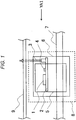
- FIGS. 1 and 2 illustrate an example in which a current sensor 8 according to the present embodiment has been implemented in an inverter device.
- FIG. 2 is a view taken along the arrow YA1 of FIG. 1 .
- a bus bar 7 is made of a conductor such as copper.
- the bus bar 7 is a part of a main circuit of the inverter. Current output from a power module or the like flows in the bus bar 7. When the current flows in the bus bar 7, magnetic flux is generated, centering on the bus bar 7.
- the current sensor 8 detects the magnetic flux generated by the current flowing in the bus bar 7 and outputs a detection signal to an inverter circuit board 9.
- the inverter circuit board 9 is a control board of the inverter and performs feedback control with use of the detection signal received from the current sensor 8.
- the current sensor 8 includes a current sensor circuit 1, a current sensor board 2, a communication terminal 3, a peripheral electronic component 4, a magnetic shield 5, and a structure mold 6.
- the communication terminal 3 is a terminal that electrically connects the current sensor circuit 1 to the inverter circuit board 9.
- the communication terminal 3 transmits a signal of the current sensor circuit 1 to the inverter circuit board 9.
- the communication terminal 3 also transmits a signal from the inverter circuit board 9 to the current sensor circuit 1. Details of transmission of the signal from the inverter circuit board 9 to the current sensor circuit 1 will be described below.
- the communication terminal 3 further transmits electric power for use in operation of the current sensor circuit 1.
- the current sensor circuit 1 detects the magnetic flux generated by the current flowing in the bus bar 7 and outputs a detection signal to the inverter circuit board 9 via the communication terminal 3. Details of the current sensor circuit 1 will be described below.
- the peripheral electronic component 4 is a peripheral RC chip component mounted on the current sensor board 2.
- the current sensor board 2 is a board on which the current sensor circuit 1, the communication terminal 3, and the peripheral electronic component 4 are mounted.
- the current sensor board 2 is fixed to the bus bar 7 via the structure mold 6 so that the current sensor circuit 1 may be located away from the bus bar 7 as much as a predetermined distance.
- the magnetic shield 5 is provided to decrease an influence of a magnetic noise. As illustrated in FIG. 2 , the magnetic shield 5 is formed in a rectangular U shape to surround the bus bar 7 and the current sensor board 2.
- the structure mold 6 is a structure mold that structurally holds the current sensor board 2, the magnetic shield 5, and a part of the bus bar 7.
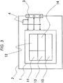
- FIG. 3 illustrates the current sensor circuit 1 and peripheral components thereof.
- the current sensor circuit 1 includes a magnetic flux detection unit 11, a signal adjustment unit 12, a control unit 13, a communication unit 14, and a memory 15.
- the control unit 13 controls operations of the respective other components of the current sensor circuit 1.
- the memory 15 is a data-rewritable memory such as an EEPROM.
- the memory 15 stores setting data including offset data and output gain data.
- the setting data stored in the memory 15 is output to the signal adjustment unit 12 by the control unit 13 as needed. Also, at the time of below-mentioned calibration of the setting data, the setting data stored in the memory 15 is corrected by the control unit 13.
- the magnetic flux detection unit 11 detects current flowing in the bus bar 7. Specifically, the magnetic flux detection unit 11 includes a hall element and detects magnetic flux generated by the current flowing in the bus bar 7 by means of the hall element to detect the current flowing in the bus bar 7. The magnetic flux detection unit 11 then outputs a voltage signal corresponding to the magnitude of the detected current to the signal adjustment unit 12.
- the signal adjustment unit 12 generates a detection signal based on the resultant current detected by the magnetic flux detection unit 11 and the setting data stored in the memory 15. Specifically, the signal adjustment unit 12 generates the detection signal by doing offset adjustment and gain adjustment of the voltage signal received from the magnetic flux detection unit 11 based on the setting data stored in the memory 15 and output from the control unit 13.
- the signal adjustment unit 12 is designed to erase stored setting data each time the electric power supply is stopped. Thus, the signal adjustment unit 12 receives setting data from the control unit 13 each time the current sensor circuit 1 is activated.
- the communication unit 14 outputs the detection signal obtained from the signal adjustment unit 12 to the inverter circuit board 9 (refer to FIG. 1 ) via the communication terminal 3.
- the communication unit 14 also receives correction data for correcting the setting data from an outside via the communication terminal 3 at the time of the calibration of the setting data stored in the memory 15. That is, the communication terminal 3 is used when the communication unit 14 outputs the detection signal and receives the correction data.
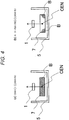
- FIGS. 4(a) and 4(b) illustrates a distribution of magnetic flux density B generated in the bus bar 7 when current flows in the bus bar 7.
- FIG. 4(a) illustrates a case in which direct current flows while FIG. 4(b) illustrates a case in which alternating current flows.
- the current density in the bus bar 7 is distributed uniformly.
- the magnetic flux density B is also distributed uniformly as illustrated in FIG. 4(a) .
- the magnetic flux density B is also concentrated on the corners of the bus bar 7 as illustrated in FIG. 4(b) .
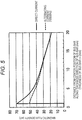
- FIG. 5 illustrates a result of current flow under each of the conditions illustrated in FIGS. 4(a) and 4(b) and illustrates magnetic flux density against a distance from a center position CEN of the bus bar 7 illustrated in each of FIGS. 4(a) and 4(b) along a thickness direction of the bus bar 7 (refer to FIGS. 4(a) and 4(b) ).
- the solid-line graph in FIG. 5 represents the result of direct current illustrated in FIG. 4(a) .
- the dashed-line graph in FIG. 5 represents the result of alternating current (frequency: 10000 Hz) illustrated in FIG. 4(b) .
- FIG. 5 illustrates a result of current flow under each of the conditions illustrated in FIGS. 4(a) and 4(b) and illustrates magnetic flux density against a distance from a center position CEN of the bus bar 7 illustrated in each of FIGS. 4(a) and 4(b) along a thickness direction of the bus bar 7 (refer to FIGS. 4(a) and 4
- a larger difference occurs in the magnetic flux density between the alternating current and the direct current at a closer position to the center position CEN.
- a detection value of the alternating current differs from a detection value of the direct current as much as the magnetic flux density of 3 mT or so. Since such a difference is generated, it is not preferable to perform calibration using direct current and then detect alternating current. That is, in a case in which alternating current is to be detected, calibration for this needs to be performed using alternating current.
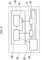
- FIG. 6 illustrates calibration according to the present embodiment.
- a calibration device 20 has a configuration from which the current sensor 8 (product sensor) to be calibrated is at least eliminated. That is, the calibration device 20 includes a current sensor calibration unit 25, an alternating current generation unit 24, a bus bar 22, and a reference current sensor 29.
- the current sensor calibration unit 25 includes a current sensor output comparison unit 26, a current sensor communication unit 27, and a switch 21.
- the reference current sensor 29 is a reference current sensor that can detect current flowing in the bus bar 22 with high accuracy.
- the bus bar 22 is made of a conductor such as copper.
- the bus bar 22 is connected to the alternating current generation unit 24 at both ends thereof.
- the reference current sensor 29 and the current sensor 8 detect alternating current flowing in the bus bar 22 (below-mentioned calibration alternating current) and output detection signals to the current sensor output comparison unit 26.
- the alternating current generation unit 24 is a single-phase alternating current generation source and mainly includes a not-illustrated voltage adjustment unit and a not-illustrated transformer.
- the alternating current generation unit 24 communicates with the current sensor output comparison unit 26 to receive an instruction from the current sensor output comparison unit 26 and output alternating current to the bus bar 22. This alternating current will be referred to as calibration alternating current.
- the current sensor output comparison unit 26 instructs the alternating current generation unit 24 to output the calibration alternating current at the time of below-mentioned output gain adjustment.
- the current sensor output comparison unit 26 compares an output of the reference current sensor 29 with an output of the current sensor 8 and outputs the difference of the output voltage to the current sensor communication unit 27.
- the current sensor communication unit 27 generates the correction data for correcting the setting data stored in the memory 15 of the current sensor 8 based on the aforementioned difference of the output voltage and outputs the correction data to the current sensor 8.
- the current sensor 8 corrects the setting data stored in the memory 15 with use of the correction data.
- the switch 21 switches between the current sensor output comparison unit 26 and the current sensor communication unit 27 as a destination of the current sensor 8.
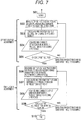
- FIG. 7 is a flowchart of calibration according to the present embodiment.
- the flowchart includes an offset voltage adjustment process consisting of steps S02 to S05 and an output gain adjustment process consisting of steps S06 to S09.
- the product sensor in FIG. 7 refers to the current sensor 8
- the reference sensor refers to the reference current sensor 29.
- a procedure of the calibration according to the present embodiment will be described with reference to FIG. 7 .
- step S01 When the calibration flow is started (step S01), the procedure moves to step S02. In step S02, no current flows in the bus bar 22. In this state, the current sensor output comparison unit 26 measures respective offset voltage of the current sensor 8 and the reference current sensor 29. After step S02, the procedure moves to step S03.
- step S03 the current sensor output comparison unit 26 subtracts the offset voltage of the reference current sensor 29 from the offset voltage of the current sensor 8 to calculate an offset voltage error.
- the current sensor output comparison unit 26 transmits offset correction data including the offset voltage error to the current sensor communication unit 27.
- step S04 the current sensor communication unit 27 outputs the aforementioned offset correction data to the current sensor 8.
- the control unit 13 corrects the offset data of the setting data stored in the memory 15 with use of the aforementioned offset correction data. Specifically, the control unit 13 adds the offset voltage error to the offset data of the setting data.
- step S05 the procedure moves to step S05.
- step S05 the current sensor output comparison unit 26 measures respective offset voltage of the current sensor 8 and the reference current sensor 29 in a state of no electric conduction to the bus bar 22 in a similar manner to step S02.
- the current sensor output comparison unit 26 then checks if the voltage value of the offset voltage of the current sensor 8 falls within a targeted output range. That is, the current sensor output comparison unit 26 determines if the difference derived by subtracting the offset voltage of the reference current sensor 29 from the offset voltage of the current sensor 8 is equal to or less than a predetermined value. In a case of affirmative determination, the procedure moves to step S06. In a case of negative determination, the procedure moves to step S02, and the similar procedure follows. In a case in which the negative determination is given a predetermined number of times, such as five times, in step S05, the current sensor 8 is determined to be a defective product.
- step S06 the alternating current generation unit 24 provides the bus bar 22 with the calibration alternating current in response to an instruction of the current sensor output comparison unit 26.
- the frequency of the calibration alternating current is a frequency for the time when the current sensor 8 is actually used, that is, a frequency of alternating current to be measured. Also, due to a below-mentioned reason (refer to FIG. 9 ), the amplitude of the calibration alternating current is set to amplitude of the maximum current to be provided to the bus bar 22 when the current sensor 8 is actually used.
- the current sensor output comparison unit 26 measures respective output voltage waveforms output from the current sensor 8 and the reference current sensor 29. After step S06, the procedure moves to step S07.
- step S07 the current sensor output comparison unit 26 calculates an output gain error from the voltage waveforms of the current sensor 8 and the reference current sensor 29.
- the current sensor output comparison unit 26 transmits output gain correction data including the output gain error to the current sensor communication unit 27.
- step S07 the procedure moves to step S08.
- step S08 the current sensor communication unit 27 outputs the aforementioned output gain correction data to the current sensor 8.
- the control unit 13 corrects the output gain data of the setting data stored in the memory 15 with use of the aforementioned output gain correction data. Specifically, the control unit 13 adds the output gain error to the output gain data of the setting data.
- step S09 the procedure moves to step S09.
- step S09 the current sensor output comparison unit 26 measures respective output voltage waveforms of the current sensor 8 and the reference current sensor 29 in a state in which the calibration alternating current flows in the bus bar 22 in a similar manner to step S06.
- the current sensor output comparison unit 26 then checks if the voltage amplified by the output gain of the current sensor 8 falls within a targeted output range. That is, the current sensor output comparison unit 26 determines if the difference between the amplitude of the output voltage waveform of the current sensor 8 and the amplitude of the output voltage waveform of the reference current sensor 29 is equal to or less than a predetermined value. In a case of affirmative determination, the procedure moves to step S10 to end the flow.
- step S06 In a case of negative determination, the procedure moves to step S06, and the similar procedure follows .
- the negative determination is given a predetermined number of times, such as five times, in step S09, the current sensor 8 is determined to be a defective product.
- the corrected setting data based on the detection value of the predetermined calibration alternating current detected by the magnetic flux detection unit 11 is stored in the memory 15.
- a detection error can be prevented from being generated when the current sensor 8 detects the alternating current.
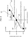
- FIG. 8 illustrates an example of a relationship between input current and output voltage of the current sensor 8 at the time of calibration using direct current.
- the current needs to be provided until the measurement is completed in a state in which the current is stable.
- calibration using a maximum current value 700 A in FIG. 8
- calibration along a dashed line L1 is supposed to be performed, calibration along a solid line L2 may actually be performed.
- FIG. 9 illustrates an example of a relationship between input current and output voltage of the current sensor 8 at the time of calibration according to the present embodiment.
- calibration is performed using alternating current having the maximum amplitude of 700A, which may actually be used.
- the frequency of the alternating current is set to a frequency that is to be used actually.
- calibration can be performed at a current area that is to be used actually, which is a range of from -700 A to +700 A. That is, at the entire current area to be used actually, voltage to be output from the current sensor 8 can have no error.
- the current sensor according to the present embodiment is configured in the following manner and has the following effects.
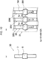
- FIG. 10(a) illustrates a current detection unit 30.
- the current detection unit 30 is a unit in which the current sensor 8 is provided on the bus bar 7 and in which the current sensor 8 detects current flowing in the bus bar 7.
- the current detection unit 30 constitutes a current detection module 31 as illustrated in FIG. 10(b) .
- the current detection module 31 includes as many current detection units 30 as the number of phases of alternating current to be used.
- FIG. 10(b) illustrates the current detection module 31 for three-phase alternating current. Since the current detection module 31 illustrated in FIG. 10(b) is configured to let three-phase alternating current flow, the current detection module 31 includes three current detection units 30. For the following description, reference signs of the three current detection units 30 illustrated in FIG.
- 10(b) will be 30U, 30V, and 30W, respectively.
- reference signs of the bus bars included in the current detection units 30U, 30V, and 30W will be 7U, 7V, and 7W, respectively.
- Reference signs of the current sensors included in the current detection units 30U, 30V, and 30W will be 8U, 8V, and 8W, respectively.
- FIG. 10(b) illustrates a state in which three-phase alternating current flows in the current detection module 31.
- U-phase, V-phase, and W-phase alternating current flows in the bus bars 7U, 7V, and 7W of the current detection units 30U, 30V, and 30W, respectively. That is, phases of alternating current flowing in the respective current detection units 30 differ from each other.
- Solid lines 801a, 801b, and 801c illustrated in FIG. 11 represent voltage waveforms that the current detection module 31 illustrated in FIG. 10(b) outputs.
- the current detection units 30U, 30V, and 30W of the current detection module 31 are supposed to output voltage waveforms represented by dashed lines 802a, 802b, and 802c, respectively.
- the current detection units 30U, 30V, and 30W output the solid lines 801a, 801b, and 801c.
- the current detection module 31 is constituted by three current detection units 30 each of which is calibrated using single-phase alternating current and detects three-phase alternating current, an error as much as a difference between the solid line and the dashed line will be generated. Under such circumstances, in the present embodiment, calibration is performed using three-phase alternating current with use of three current sensors 8.
- FIG. 12 illustrates calibration according to the present embodiment. Calibration according to the present embodiment will be described with reference to FIG. 12 . Description of similar components to those in the first embodiment will be omitted.
- calibration is performed using three-phase alternating current. This is a main difference from the calibration according to the first embodiment ( FIG. 6 ) .
- a calibration device 120 has a configuration from which the current sensors 8U, 8V, and 8W (product sensors) to be calibrated are at least eliminated. That is, the calibration device 120 includes a current sensor calibration unit 125, an alternating current generation unit 124, a bus bar 122, and reference current sensors 129U, 129V, and 129W. Meanwhile, the current sensor calibration unit 125 includes a current sensor output comparison unit, a current sensor communication unit, and a switch fitted to three-phase alternating current detection although these are not illustrated.
- the bus bar 122 includes bus bars 122U, 122V, and 122W. Respective first ends of the bus bars 122U, 122V, and 122W are connected to each other at a point 122P while respective second ends thereof are connected to the alternating current generation unit 124.
- the bus bars 122U, 122V, and 122W are provided with the reference current sensors 129U, 129V, and 129W and the current sensors 8U, 8V, and 8W to be calibrated, respectively.
- the alternating current generation unit 124 outputs three-phase alternating current in response to an instruction of the current sensor calibration unit 125.
- the current sensor according to the present embodiment is configured in the following manner and has the following effects in addition to the effects according to the first embodiment.
- the magnetic flux detection unit 11 detects magnetic flux generated by three-phase alternating current flowing in the three bus bars to respectively detect the three-phase alternating current flowing in the three bus bars.
- Calibration alternating current is also three-phase alternating current corresponding to the targets to be measured, and current of the respective phases flows in the three respective bus bars.
- FIG. 13 illustrates a power inversion device 50 (inverter device 50) including the current sensor 8.
- the current sensor 8 is provided in the current detection module 31 for detection of three-phase alternating current as illustrated in FIG. 10 (b) .
- the current detection module 31 is provided in the power inversion device 50 to cause the current sensor 8 to be provided in the power inversion device 50.
- the power inversion device 50 includes the current detection module 31, an inverter circuit 51, a smoothing capacitor 52, an inverter circuit board 59, and terminals P1, P2, P3, P4, P5, P6, and P7.
- Respective first ends of the bus bars 7U, 7V, and 7W of the current detection module 31 on the right side of the figure are connected to the terminals P5, P6, and P7, respectively.
- loads such as three-phase motors are normally connected to the terminals P5, P6, and P7.
- respective second ends of the bus bars 7U, 7V, and 7W of the current detection module 31 on the left side of the figure are connected to output terminals 51U, 51V, and 51W of the inverter circuit 51, respectively.
- the inverter circuit 51 is connected via the smoothing capacitor 52 and the terminal P1 to a not-illustrated high-voltage power source and is supplied from the high-voltage power source with power to be output to an outside via the terminals P5, P6, and P7.
- the inverter circuit 51 includes high-side U-phase switch UH, V-phase switch VH, and W-phase switch WH and low-side U-phase switch UL, V-phase switch VL, and W-phase switch WL. These switches are controlled by a control circuit 53.
- the inverter circuit board 59 includes the control circuit 53 and a switch 54.
- the control circuit 53 is supplied from a not-illustrated low-voltage power source with low-voltage power via the terminal P3.
- the control circuit 53 receives a control communication signal from a not-illustrated control device via the terminal P2 and is operated.
- the control circuit 53 controls the switch 54 as well as the switches UH, VH, WH, UL, VL, and WL included in the inverter circuit 51.
- the switch 54 is controlled so that the switch 54 may be turned off in a case of below-mentioned calibration and may be turned on in the other cases (normal cases).
- the control circuit 53 receives detection signals from the current sensors 8U, 8V, and 8W in normal cases.
- the reason for turning off the switch 54 in the case of calibration is to prevent a signal of the communication terminal 3 from being input in the control circuit 53 to enable the setting data of the current sensor 8 to be corrected (rewritten) normally by a calibration device.
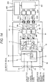
- FIG. 14 illustrates calibration according to the present embodiment.
- the current sensors 8U, 8V, and 8W are calibrated by attaching a calibration device 220 to the power inversion device 50.
- the calibration device 220 includes a current sensor calibration unit 225, an alternating current generation unit 224, bus bars 222U, 222V, and 222W, and reference current sensors 229U, 229V, and 229W.
- the current sensor calibration unit 225 includes a current sensor output comparison unit, a current sensor communication unit, and a switch fitted to three-phase alternating current detection although these are not illustrated.
- the bus bars 222U, 222V, and 222W of the calibration device 220 are connected to the terminals P5, P6, and P7 of the power inversion device 50, respectively.
- Three-phase calibration alternating current generated from the alternating current generation unit 224 is input via the bus bars 222U, 222V, and 222W and the terminals P5, P6, and P7 to the power inversion device 50, respectively.
- the three-phase calibration alternating current flows in the bus bars 7U, 7V, and 7W.
- detection signals output from the current sensors 8U, 8V, and 8W of the power inversion device 50 are input in the current sensor calibration unit 225.
- Output signals of the reference current sensors 229U, 229V, and 229W are also input in the current sensor calibration unit 225.
- the current sensor calibration unit 225 calculates differences between the detection signals of the current sensors 8U, 8V, and 8W and the output signals of the reference current sensors 229U, 229V, and 229W in terms of the U phase, V phase, and W phase, respectively. Based on the differences, the current sensor calibration unit 225 generates correction data for correcting the setting data of the respective phases and outputs the correction data to the current sensors 8U, 8V, and 8W, respectively.
- the switch 54 is controlled so that the switch 54 may be turned off at the time of correcting the setting data stored in the memory 15 of the current sensor circuit 1 of the current sensor 8, that is, at the time of calibration. After the switch 54 is turned off to disconnect the calibration device 220 from the control circuit 53, the calibration device 220 corrects the aforementioned setting data.
- the current sensor according to the present embodiment is configured in the following manner and has the following effects.
- the current sensor 8 is mounted on the power inversion device 50 including the inverter circuit 51 including the plurality of switching elements UH, UL, VH, VL, WH, and WL, the inverter direct-current terminal P1 electrically connected to the inverter circuit 51, and the inverter alternating-current terminals P5, P6, and P7 electrically connected to the inverter circuit 51.
- the plurality of bus bars 7U, 7V, and 7W are connected to the inverter circuit 51 and the inverter alternating-current terminals P5, P6, and P7.
- the respective switching elements UH, UL, VH, VL, WH, and WL of the inverter circuit 51 are in predetermined switch states . That is, the high-side U-phase switch UH, V-phase switch VH, and W-phase switch WH are turned off. Conversely, the low-side U-phase switch UL, V-phase switch VL, and W-phase switch WL are turned on.
- the current sensor 8 can be calibrated without disconnecting the current sensor 8 from the power inversion device 50. Also, unlike the second embodiment, since the current sensor 8 is calibrated in the power inversion device 50, on which the current sensor 8 is actually mounted, calibration can be performed under conditions more similar to actual use environment conditions (for example, conditions such as a magnetic flux density distribution).
- FIG. 15 illustrates calibration according to the present embodiment.
- the current sensor 8 is mounted on the power inversion device 50 illustrated in FIG. 13 and is calibrated in this state.
- a calibration device 320 includes no alternating current generation unit, the calibration device 320 is connected to a motor M as well, and calibration is performed using alternating current output from the power inversion device 50. Description of similar components to those in the third embodiment will be omitted.
- the current sensor 8 is calibrated when the power inversion device 50 outputs alternating current to the motor M serving as a load.
- the calibration device 320 according to the present embodiment is provided between the power inversion device 50 and the motor M. First ends of winding wires 61, 62, and 63 of the motor M are connected to the calibration device 320 while second ends of the winding wires 61, 62, and 63 are connected to each other.
- the calibration device 320 includes a current sensor calibration unit 325, bus bars 322U, 322V, and 322W, and reference current sensors 329U, 329V, and 329W. That is, the calibration device 320 includes no alternating current generation unit.
- high-voltage power of the power inversion device 50 from the high-voltage power source is used.
- the control circuit 53 controls the switches UH, UL, VH, VL, WH, and WL so that the inverter circuit 51 may output three-phase alternating current.
- the alternating current output from the inverter circuit 51 flows in the bus bars 7U, 7V, and 7W, passes through the terminals P5, P6, and P7, flows in the bus bars 322U, 322V, and 322W of the calibration device 320, and reaches the U-phase winding wire 61, V-phase winding wire 62, and W-phase winding wire 63 of the motor M.
- detection signals output from the current sensors 8U, 8V, and 8W of the power inversion device 50 are input in the current sensor calibration unit 325.
- Output signals of the reference current sensors 329U, 329V, and 329W are also input in the current sensor calibration unit 325.
- the current sensor calibration unit 325 calculates differences between the detection signals of the current sensors 8U, 8V, and 8W and the output signals of the reference current sensors 329U, 329V, and 329W in terms of the U phase, V phase, and W phase, respectively. Based on the differences, the current sensor calibration unit 325 generates correction data for correcting the setting data of the respective phases and outputs the correction data to the current sensors 8U, 8V, and 8W, respectively.
- the switch 54 is controlled so that the switch 54 may be turned off at the time of correcting the setting data stored in the memory 15 of the current sensor circuit 1 of the current sensor 8, that is, at the time of calibration. After the switch 54 is turned off to disconnect the calibration device 320 from the control circuit 53, the calibration device 220 corrects the aforementioned setting data.
- the current sensor according to the present embodiment is configured in the following manner and has the following effects.
- the current sensor 8 is mounted on the power inversion device 50 including the inverter circuit 51 including the plurality of switching elements UH, UL, VH, VL, WH, and WL for inverting direct current into alternating current and the inverter output terminals P5, P6, and P7 for outputting alternating current.
- the plurality of bus bars 7U, 7V, and 7W are connected to the inverter circuit 51 and the inverter output terminals P5, P6, and P7.
- calibration is performed using alternating current that the power inversion device 50 actually outputs. Since a target to be measured by the current sensor 8 is this alternating current, an error can be prevented from being included in a detection signal that the current sensor 8 outputs further than in the third embodiment.
- the structure mold 6 illustrated in FIGS. 1 and 2 is fixed to the bus bar 7, the present invention is not limited to this.
- the structure mold 6 may be fixed to the inverter circuit board 9 or may be provided integrally with a mold member included in the inverter circuit board 9.
- the current sensor board illustrated in FIGS. 1 and 2 is separated from the inverter circuit board, the current sensor board may be provided integrally with the inverter circuit board.
- the magnetic shield 5 illustrated in FIG. 2 is formed in the rectangular U shape, the present invention is not limited to this.
- the magnetic shield 5 may be in a round U shape or in a shield shape divided into plural pieces.
- the memory 15 of the current sensor 8 may be able to store setting data for a plurality of frequencies.
- one or a plurality of frequencies can be used for alternating current for use in calibration.
- one of the frequencies may be zero, that is, may be applied to direct current.
- the magnetic flux detection unit 11 in FIG. 3 may include a magnetic flux detection element other than the hall element.
- the magnetic flux detection unit 11 may include a giant magnetoresistance element (GMR element).
- GMR element giant magnetoresistance element
- the present invention is not limited to this.
- the present invention can be applied when multiphase alternating current of N (N is an integer of at least two) phases is targeted for measurement. Also, as described in the first embodiment, the present invention can be applied when single-phase alternating current is targeted for measurement.
- the setting data (offset data and output gain data) stored in the memory 15 is corrected based on the correction data received from the current sensor communication unit 27 of the calibration device 20 to calibrate the current sensor 8.
- the setting data and the correction data may be stored in the memory 15, and based on the data, the calibrated setting data may be output from the control unit 13 to the signal adjustment unit 12.
Landscapes
- Physics & Mathematics (AREA)
- General Physics & Mathematics (AREA)
- Inverter Devices (AREA)
- Measuring Instrument Details And Bridges, And Automatic Balancing Devices (AREA)
- Measurement Of Current Or Voltage (AREA)
Applications Claiming Priority (2)
| Application Number | Priority Date | Filing Date | Title |
|---|---|---|---|
| JP2015022254 | 2015-02-06 | ||
| PCT/JP2016/052223 WO2016125638A1 (fr) | 2015-02-06 | 2016-01-27 | Capteur de courant électrique |
Publications (2)
| Publication Number | Publication Date |
|---|---|
| EP3255441A1 true EP3255441A1 (fr) | 2017-12-13 |
| EP3255441A4 EP3255441A4 (fr) | 2018-12-12 |
Family
ID=56563988
Family Applications (1)
| Application Number | Title | Priority Date | Filing Date |
|---|---|---|---|
| EP16746469.2A Withdrawn EP3255441A4 (fr) | 2015-02-06 | 2016-01-27 | Capteur de courant électrique |
Country Status (5)
| Country | Link |
|---|---|
| US (1) | US20180017656A1 (fr) |
| EP (1) | EP3255441A4 (fr) |
| JP (1) | JP6513715B2 (fr) |
| CN (1) | CN107209209A (fr) |
| WO (1) | WO2016125638A1 (fr) |
Cited By (1)
| Publication number | Priority date | Publication date | Assignee | Title |
|---|---|---|---|---|
| EP3767311A1 (fr) * | 2019-07-15 | 2021-01-20 | Allegro MicroSystems, LLC | Procédé et appareil pour la compensation d'effet de fréquence dans des capteurs de courant de champ magnétique |
Families Citing this family (18)
| Publication number | Priority date | Publication date | Assignee | Title |
|---|---|---|---|---|
| JP6300881B1 (ja) * | 2016-10-24 | 2018-03-28 | 株式会社Naaファシリティーズ | 校正試験装置 |
| JP6840618B2 (ja) * | 2017-05-17 | 2021-03-10 | 日置電機株式会社 | トランス損失測定装置およびトランス損失測定方法 |
| JP2019070563A (ja) * | 2017-10-06 | 2019-05-09 | 株式会社デンソー | 電流センサ |
| JP7000572B2 (ja) * | 2018-07-04 | 2022-01-19 | 日立Astemo株式会社 | 電気回路装置 |
| KR102141598B1 (ko) * | 2018-11-22 | 2020-08-05 | 주식회사 아이티엑스엠투엠 | 시스템 정보를 이용한 보정 기능을 갖는 전류 측정 장치 및 방법 |
| KR102148159B1 (ko) * | 2018-11-22 | 2020-10-14 | 주식회사 아이티엑스에이아이 | 히스테리시스 오차 보정 기능을 갖는 전류 측정 장치 및 방법 |
| JP7172509B2 (ja) * | 2018-11-29 | 2022-11-16 | Tdk株式会社 | 異常検出装置および電力変換装置 |
| KR102497448B1 (ko) * | 2019-02-14 | 2023-02-08 | 주식회사 엘지에너지솔루션 | 배터리 셀 이상 판단 장치 및 방법 |
| JP7259632B2 (ja) * | 2019-08-09 | 2023-04-18 | Tdk株式会社 | 電流センサ |
| DE102019124405A1 (de) | 2019-09-11 | 2021-03-11 | Schaeffler Technologies AG & Co. KG | Stromsensor |
| JP7244403B2 (ja) * | 2019-11-20 | 2023-03-22 | Necプラットフォームズ株式会社 | 校正方法及び導出システム |
| DE102019132593B4 (de) | 2019-12-02 | 2021-07-22 | Schaeffler Technologies AG & Co. KG | Stromsensor |
| DE102020100297B4 (de) | 2020-01-09 | 2023-01-19 | Schaeffler Technologies AG & Co. KG | Stromsensor und elektrisches System mit dem Stromsensor |
| JP7605597B2 (ja) * | 2020-08-05 | 2024-12-24 | 横河電機株式会社 | 電流測定装置 |
| DE102020215561A1 (de) | 2020-12-09 | 2022-06-09 | Zf Friedrichshafen Ag | Leiterplattenanordnung und Bauteilanordnung zur Positionierung von Stromsensoren, sowie Montageverfahren |
| DE102021127855A1 (de) * | 2021-06-11 | 2022-12-22 | Methode Electronics Malta Ltd. | Stromsensor, der einen Magnetfeldsensor in einer V-förmigenAnordnung umfasst |
| JP7224513B1 (ja) * | 2022-05-10 | 2023-02-17 | 三菱電機株式会社 | 電力変換装置 |
| DE102023210574A1 (de) * | 2023-10-26 | 2025-04-30 | Zf Friedrichshafen Ag | Kalibrieren von Stromsensoren in Invertern mit Wechselstrom |
Family Cites Families (22)
| Publication number | Priority date | Publication date | Assignee | Title |
|---|---|---|---|---|
| US4130796A (en) * | 1977-12-07 | 1978-12-19 | Westinghouse Electric Corp. | Calibrating and measuring circuit for a capacitive probe-type instrument |
| JP2004180490A (ja) * | 2002-11-15 | 2004-06-24 | Ebara Densan Ltd | 系統連系インバータ装置の直流分検知回路及び検知システム |
| ATE443873T1 (de) * | 2004-11-18 | 2009-10-15 | Powersense As | Kompensation von einfachen faseroptischen faraday-effekt-sensoren |
| US7511468B2 (en) * | 2006-11-20 | 2009-03-31 | Mceachern Alexander | Harmonics measurement instrument with in-situ calibration |
| JP4897582B2 (ja) * | 2007-06-15 | 2012-03-14 | 中国電力株式会社 | マルチトランスデューサ及びその制御方法 |
| JP2009250666A (ja) * | 2008-04-02 | 2009-10-29 | Daihen Corp | オフセット信号検出回路、このオフセット信号検出回路を用いた信号検出装置および電流信号検出装置 |
| JP2011185775A (ja) * | 2010-03-09 | 2011-09-22 | Aisin Aw Co Ltd | 電流検出装置 |
| US8847577B2 (en) * | 2010-08-04 | 2014-09-30 | Sensus Spectrum Llc | Method and system of measuring current in an electric meter |
| US8531141B2 (en) * | 2011-02-28 | 2013-09-10 | Deere & Company | System for calibrating an electrical control system |
| JP2012184985A (ja) * | 2011-03-04 | 2012-09-27 | Panasonic Corp | 分散型発電システム |
| US8508212B2 (en) * | 2011-06-14 | 2013-08-13 | International Business Machines Corporation | Calibration of non-contact current sensors |
| DE102011078334A1 (de) * | 2011-06-29 | 2013-01-03 | Robert Bosch Gmbh | Verfahren und System zum Kalibrieren eines Shunt-Widerstands |
| CN103765230A (zh) * | 2011-08-31 | 2014-04-30 | 本田技研工业株式会社 | 电流检测电路模块 |
| EP2587268A1 (fr) * | 2011-10-26 | 2013-05-01 | LEM Intellectual Property SA | Transducteur de courant électrique |
| US9310398B2 (en) * | 2011-11-29 | 2016-04-12 | Infineon Technologies Ag | Current sensor package, arrangement and system |
| KR101238943B1 (ko) * | 2011-12-19 | 2013-03-04 | 엘에스산전 주식회사 | 전류센서의 옵셋 보상 장치 및 방법 |
| JP5629302B2 (ja) * | 2012-02-29 | 2014-11-19 | 旭化成エレクトロニクス株式会社 | 自己診断機能を有する電流センサ及び信号処理回路 |
| KR20140115586A (ko) * | 2013-03-21 | 2014-10-01 | 삼성전자주식회사 | 이동식 소모 전류 측정 장치, 전류 측정 단말 및 소모 전류 측정 방법 |
| GB201309825D0 (en) * | 2013-06-01 | 2013-07-17 | Metroic Ltd | Current measurement |
| DE102013213508A1 (de) * | 2013-07-10 | 2015-01-15 | Dr. Johannes Heidenhain Gmbh | Verfahren und Vorrichtung zur Strommessung an einem Umrichter |
| US9823328B2 (en) * | 2014-08-01 | 2017-11-21 | Dell Products Lp | Systems and methods of current sense calibration for voltage regulator circuits |
| US9671438B2 (en) * | 2014-11-05 | 2017-06-06 | Qualcomm Incorporated | High-current sensing scheme using drain-source voltage |
-
2016
- 2016-01-27 US US15/548,546 patent/US20180017656A1/en not_active Abandoned
- 2016-01-27 JP JP2016573298A patent/JP6513715B2/ja active Active
- 2016-01-27 CN CN201680006504.1A patent/CN107209209A/zh active Pending
- 2016-01-27 EP EP16746469.2A patent/EP3255441A4/fr not_active Withdrawn
- 2016-01-27 WO PCT/JP2016/052223 patent/WO2016125638A1/fr not_active Ceased
Cited By (2)
| Publication number | Priority date | Publication date | Assignee | Title |
|---|---|---|---|---|
| EP3767311A1 (fr) * | 2019-07-15 | 2021-01-20 | Allegro MicroSystems, LLC | Procédé et appareil pour la compensation d'effet de fréquence dans des capteurs de courant de champ magnétique |
| US11047928B2 (en) | 2019-07-15 | 2021-06-29 | Allegro Microsystems, Llc | Methods and apparatus for frequency effect compensation in magnetic field current sensors |
Also Published As
| Publication number | Publication date |
|---|---|
| JPWO2016125638A1 (ja) | 2017-09-14 |
| EP3255441A4 (fr) | 2018-12-12 |
| JP6513715B2 (ja) | 2019-05-15 |
| CN107209209A (zh) | 2017-09-26 |
| WO2016125638A1 (fr) | 2016-08-11 |
| US20180017656A1 (en) | 2018-01-18 |
Similar Documents
| Publication | Publication Date | Title |
|---|---|---|
| EP3255441A1 (fr) | Capteur de courant électrique | |
| KR101956406B1 (ko) | 전류를 측정하기 위한 디바이스 | |
| FI124174B (fi) | Maasulkuvirran mittaaminen | |
| CN101634668B (zh) | 多相直流/直流升压转换器的电流感测 | |
| US20110221366A1 (en) | Methods, systems and apparatus for synchronous current regulation of a five-phase machine | |
| US20180156847A1 (en) | Current detection device | |
| KR20180008790A (ko) | 전력 변환 장치 및 모터 구동 장치 | |
| US12481015B2 (en) | Method and apparatus for calibrating a measurement device | |
| JP2010175276A (ja) | 磁気比例式電流センサ | |
| US9318983B2 (en) | Motor controller | |
| US7453231B2 (en) | Electric vehicle control device | |
| US9197125B2 (en) | Method for limiting startup currents in an inverter circuit | |
| JP6621530B2 (ja) | 電流検出装置 | |
| EP3889619A1 (fr) | Dispositif de détection de courant | |
| KR20210127545A (ko) | 전류 센서, 조향 제어 장치 및 전류 검출 방법 | |
| CN110176864A (zh) | 电力变换装置 | |
| CN102158108B (zh) | 用于操作变换器电路的方法以及用于实施该方法的装置 | |
| CN104040869B (zh) | 用于校准多相逆变器的方法、用于运行的设备 | |
| US20230009497A1 (en) | Method for operating an electric machine | |
| JP2014055839A (ja) | 電流検出装置 | |
| CN111796168A (zh) | 绝缘测试装置及其方法 | |
| JP3261476B2 (ja) | 電圧検出回路 | |
| JP5871132B2 (ja) | 電力計測ユニットおよび分電盤 | |
| JP6658501B2 (ja) | バッテリ充電回路 | |
| KR101393574B1 (ko) | 모터의 전력 케이블의 단선 검출 방법 및 모터 제어 방법 |
Legal Events
| Date | Code | Title | Description |
|---|---|---|---|
| STAA | Information on the status of an ep patent application or granted ep patent |
Free format text: STATUS: THE INTERNATIONAL PUBLICATION HAS BEEN MADE |
|
| PUAI | Public reference made under article 153(3) epc to a published international application that has entered the european phase |
Free format text: ORIGINAL CODE: 0009012 |
|
| STAA | Information on the status of an ep patent application or granted ep patent |
Free format text: STATUS: REQUEST FOR EXAMINATION WAS MADE |
|
| 17P | Request for examination filed |
Effective date: 20170906 |
|
| AK | Designated contracting states |
Kind code of ref document: A1 Designated state(s): AL AT BE BG CH CY CZ DE DK EE ES FI FR GB GR HR HU IE IS IT LI LT LU LV MC MK MT NL NO PL PT RO RS SE SI SK SM TR |
|
| AX | Request for extension of the european patent |
Extension state: BA ME |
|
| DAV | Request for validation of the european patent (deleted) | ||
| DAX | Request for extension of the european patent (deleted) | ||
| RIC1 | Information provided on ipc code assigned before grant |
Ipc: G01R 19/00 20060101AFI20181031BHEP Ipc: G01R 15/20 20060101ALI20181031BHEP |
|
| A4 | Supplementary search report drawn up and despatched |
Effective date: 20181109 |
|
| STAA | Information on the status of an ep patent application or granted ep patent |
Free format text: STATUS: THE APPLICATION HAS BEEN WITHDRAWN |
|
| 18W | Application withdrawn |
Effective date: 20210215 |