EP3255443B1 - Verfahren zur schätzung der integrität eines leistungssystems - Google Patents
Verfahren zur schätzung der integrität eines leistungssystems Download PDFInfo
- Publication number
- EP3255443B1 EP3255443B1 EP17171253.2A EP17171253A EP3255443B1 EP 3255443 B1 EP3255443 B1 EP 3255443B1 EP 17171253 A EP17171253 A EP 17171253A EP 3255443 B1 EP3255443 B1 EP 3255443B1
- Authority
- EP
- European Patent Office
- Prior art keywords
- switch
- health
- voltage
- measured
- parameter
- Prior art date
- Legal status (The legal status is an assumption and is not a legal conclusion. Google has not performed a legal analysis and makes no representation as to the accuracy of the status listed.)
- Active
Links
Images


Classifications
-
- G—PHYSICS
- G01—MEASURING; TESTING
- G01R—MEASURING ELECTRIC VARIABLES; MEASURING MAGNETIC VARIABLES
- G01R31/00—Arrangements for testing electric properties; Arrangements for locating electric faults; Arrangements for electrical testing characterised by what is being tested not provided for elsewhere
- G01R31/327—Testing of circuit interrupters, switches or circuit-breakers
-
- G—PHYSICS
- G01—MEASURING; TESTING
- G01R—MEASURING ELECTRIC VARIABLES; MEASURING MAGNETIC VARIABLES
- G01R31/00—Arrangements for testing electric properties; Arrangements for locating electric faults; Arrangements for electrical testing characterised by what is being tested not provided for elsewhere
- G01R31/26—Testing of individual semiconductor devices
- G01R31/2607—Circuits therefor
- G01R31/2608—Circuits therefor for testing bipolar transistors
- G01R31/2617—Circuits therefor for testing bipolar transistors for measuring switching properties thereof
-
- G—PHYSICS
- G01—MEASURING; TESTING
- G01R—MEASURING ELECTRIC VARIABLES; MEASURING MAGNETIC VARIABLES
- G01R31/00—Arrangements for testing electric properties; Arrangements for locating electric faults; Arrangements for electrical testing characterised by what is being tested not provided for elsewhere
- G01R31/26—Testing of individual semiconductor devices
- G01R31/2607—Circuits therefor
- G01R31/2621—Circuits therefor for testing field effect transistors, i.e. FET's
-
- H—ELECTRICITY
- H02—GENERATION; CONVERSION OR DISTRIBUTION OF ELECTRIC POWER
- H02M—APPARATUS FOR CONVERSION BETWEEN AC AND AC, BETWEEN AC AND DC, OR BETWEEN DC AND DC, AND FOR USE WITH MAINS OR SIMILAR POWER SUPPLY SYSTEMS; CONVERSION OF DC OR AC INPUT POWER INTO SURGE OUTPUT POWER; CONTROL OR REGULATION THEREOF
- H02M3/00—Conversion of DC power input into DC power output
- H02M3/02—Conversion of DC power input into DC power output without intermediate conversion into AC
- H02M3/04—Conversion of DC power input into DC power output without intermediate conversion into AC by static converters
- H02M3/10—Conversion of DC power input into DC power output without intermediate conversion into AC by static converters using discharge tubes with control electrode or semiconductor devices with control electrode
- H02M3/145—Conversion of DC power input into DC power output without intermediate conversion into AC by static converters using discharge tubes with control electrode or semiconductor devices with control electrode using devices of a triode or transistor type requiring continuous application of a control signal
- H02M3/155—Conversion of DC power input into DC power output without intermediate conversion into AC by static converters using discharge tubes with control electrode or semiconductor devices with control electrode using devices of a triode or transistor type requiring continuous application of a control signal using semiconductor devices only
- H02M3/156—Conversion of DC power input into DC power output without intermediate conversion into AC by static converters using discharge tubes with control electrode or semiconductor devices with control electrode using devices of a triode or transistor type requiring continuous application of a control signal using semiconductor devices only with automatic control of output voltage or current, e.g. switching regulators
- H02M3/158—Conversion of DC power input into DC power output without intermediate conversion into AC by static converters using discharge tubes with control electrode or semiconductor devices with control electrode using devices of a triode or transistor type requiring continuous application of a control signal using semiconductor devices only with automatic control of output voltage or current, e.g. switching regulators including plural semiconductor devices as final control devices for a single load
-
- H—ELECTRICITY
- H02—GENERATION; CONVERSION OR DISTRIBUTION OF ELECTRIC POWER
- H02M—APPARATUS FOR CONVERSION BETWEEN AC AND AC, BETWEEN AC AND DC, OR BETWEEN DC AND DC, AND FOR USE WITH MAINS OR SIMILAR POWER SUPPLY SYSTEMS; CONVERSION OF DC OR AC INPUT POWER INTO SURGE OUTPUT POWER; CONTROL OR REGULATION THEREOF
- H02M7/00—Conversion of AC power input into DC power output; Conversion of DC power input into AC power output
- H02M7/02—Conversion of AC power input into DC power output without possibility of reversal
- H02M7/04—Conversion of AC power input into DC power output without possibility of reversal by static converters
- H02M7/12—Conversion of AC power input into DC power output without possibility of reversal by static converters using discharge tubes with control electrode or semiconductor devices with control electrode
- H02M7/21—Conversion of AC power input into DC power output without possibility of reversal by static converters using discharge tubes with control electrode or semiconductor devices with control electrode using devices of a triode or transistor type requiring continuous application of a control signal
- H02M7/217—Conversion of AC power input into DC power output without possibility of reversal by static converters using discharge tubes with control electrode or semiconductor devices with control electrode using devices of a triode or transistor type requiring continuous application of a control signal using semiconductor devices only
-
- H—ELECTRICITY
- H02—GENERATION; CONVERSION OR DISTRIBUTION OF ELECTRIC POWER
- H02M—APPARATUS FOR CONVERSION BETWEEN AC AND AC, BETWEEN AC AND DC, OR BETWEEN DC AND DC, AND FOR USE WITH MAINS OR SIMILAR POWER SUPPLY SYSTEMS; CONVERSION OF DC OR AC INPUT POWER INTO SURGE OUTPUT POWER; CONTROL OR REGULATION THEREOF
- H02M7/00—Conversion of AC power input into DC power output; Conversion of DC power input into AC power output
- H02M7/42—Conversion of DC power input into AC power output without possibility of reversal
- H02M7/44—Conversion of DC power input into AC power output without possibility of reversal by static converters
- H02M7/48—Conversion of DC power input into AC power output without possibility of reversal by static converters using discharge tubes with control electrode or semiconductor devices with control electrode
- H02M7/53—Conversion of DC power input into AC power output without possibility of reversal by static converters using discharge tubes with control electrode or semiconductor devices with control electrode using devices of a triode or transistor type requiring continuous application of a control signal
- H02M7/537—Conversion of DC power input into AC power output without possibility of reversal by static converters using discharge tubes with control electrode or semiconductor devices with control electrode using devices of a triode or transistor type requiring continuous application of a control signal using semiconductor devices only, e.g. single switched pulse inverters
-
- G—PHYSICS
- G01—MEASURING; TESTING
- G01R—MEASURING ELECTRIC VARIABLES; MEASURING MAGNETIC VARIABLES
- G01R31/00—Arrangements for testing electric properties; Arrangements for locating electric faults; Arrangements for electrical testing characterised by what is being tested not provided for elsewhere
- G01R31/26—Testing of individual semiconductor devices
- G01R31/2607—Circuits therefor
- G01R31/2637—Circuits therefor for testing other individual devices
-
- G—PHYSICS
- G01—MEASURING; TESTING
- G01R—MEASURING ELECTRIC VARIABLES; MEASURING MAGNETIC VARIABLES
- G01R31/00—Arrangements for testing electric properties; Arrangements for locating electric faults; Arrangements for electrical testing characterised by what is being tested not provided for elsewhere
- G01R31/40—Testing power supplies
Definitions
- the present invention relates to estimating the health of power conversion system components, and particularly the health of power electronics switches such as MOSFETs, SiC MOSFETs, and IGBTs which can be used, for example, in inverter/rectifier systems.
- power electronics switches such as MOSFETs, SiC MOSFETs, and IGBTs which can be used, for example, in inverter/rectifier systems.
- Power systems generally include power converting systems, for example inverter or rectifiers. These converters may be employed in safety critical applications such as starter generators, e-oil, e-fuel or electrical actuation systems in aero applications. In these applications, safety and reliability are of the utmost importance. They can also be used in the context of land and sea electrical/hybrid electric propulsion systems, as well as for industrial drives, solar and wind power conversion etc.
- the health of power devices has been estimated based on the threshold voltage limit of the on-stage voltage of the IGBT ( Ralf Schmidt, Felix Zeyss, and Uwe Scheuermann. Impact of absolute junction temperature on power cycling lifetime. 15th European Conference on Power Electronics and Applications (EPE), pages 1-10, 2013 ). Accelerated aging tests were performed to create thermal stress tests of the devices to induce latch-up failures, and in particular through increasing the maximum junction temperature of a given device by reducing its heat transfer capability (for example by removing the heat sink). The device was then subjected to high temperature cycling until the latch-up failure occurred. In parallel to this, the junction temperature of the device was estimated based on the power loss.
- Another approach for monitoring the health of power devices is based on the switching behaviour. It utilizes the changes in ringing behaviour during the commutation period of a power module. This requires measuring the voltage or current in the high voltage side of the inverter, and uses a bandpass filter to extract the high frequency ringing component. This approach relies on the fact that increase in the damping co-efficient and attenuation in high frequency ringing of voltage and current waveform occurs after ageing of the power modules.
- US2013328596 discloses a method including obtaining a standard value for a characteristic of a power switch and obtaining a measured value of the characteristic via a gate drive unit connected to a gate terminal of the power switch. The method also includes determining a health state of the power switch by comparing the measured value to the standard value of the characteristic.
- US2014103937 discloses systems, methods and devices which utilize Spread Spectrum Time Domain Reflectometry (SSTDR) techniques to measure degradation of electronic components. Such measurements may be implemented while the components "live” or otherwise functioning within an overall system.
- monitoring a power converter in a high power system is accomplished.
- degradation of components within the power converter e.g. metal-oxide-semiconductor field-effect transistors (MOSFETs), capacitors, insulated-gate bipolar transistors (IGBTs), and the like
- MOSFETs metal-oxide-semiconductor field-effect transistors
- IGBTs insulated-gate bipolar transistors
- an aging MOSFET may experience an increase of drain to source resistance which adds additional resistance to a current path within a power converter. Such a change is able to be analyzed monitored upon processing the reflected test signals
- WO15044205 discloses a method for determining an actual junction temperature and/or an actual collector current of an IGBT device, wherein the IGBT device has a main emitter and an auxiliary emitter. The method comprises the steps of: - measuring the characteristics of an emitter voltage drop as a difference between a main emitter voltage at the main emitter and an auxiliary emitter voltage at the auxiliary emitter during a switching operation of the IGBT device; and - determining the junction temperature and/or the collector current based on the characteristics of the emitter voltage drop.
- US2013177041 discloses a system and method for monitoring in real time the operating state of an IGBT device, to determine a junction temperature and/or the remaining lifetime of an IGBT device.
- the system includes a differential unit configured to receive a gate-emitter voltage characteristic of the IGBT device to be measured and to differentiate the gate-emitter voltage characteristic to obtain pulses correlating with edges formed by a Miller plateau phase during a switch-off phase of the IGBT device.
- the system also includes a timer unit configured to measure the time delay between the obtained pulses indicating the start and end of the Miller plateau phase during the switch-off phase of the IGBT device, and a junction temperature calculation unit configured to determine at least one of the junction temperature of the IGBT device and/or the remaining lifetime of the IGBT device based on the measured time delay.
- the invention provides a method of monitoring the health of a semiconductor power electronic switch having the steps of:
- the inventors have discovered that the health of semiconductor power electronic switches, e.g. MOSFETs, SiC MOSFETs and IGBTs can be characterised with respect to the parameters mentioned above. As is discussed below, these parameters demonstrate predicable trends as compared to the health of a semiconductor power electronic switch.
- semiconductor power electronic switches e.g. MOSFETs, SiC MOSFETs and IGBTs
- the invention provides a power conversion system including:
- the invention provides a gate driver for a semiconductor power electronic switch, suitable to be installed in a power conversion system and having:
- the invention provides a propulsion system including an electric drive, the electric drive being electrically connected to the power conversion system as set out in the second aspect.
- this may be a marine propulsion system.
- the semiconductor power electronic switch may be selected from the group consisting of: a MOSFET (metal-oxide-semiconductor field-effect transistor), a SiC MOSFET, and an IGBT (insulated-gate bipolar transistor).
- a MOSFET metal-oxide-semiconductor field-effect transistor
- SiC MOSFET silicon-oxide-semiconductor field-effect transistor
- IGBT insulated-gate bipolar transistor
- the semiconductor power electronic switch is an IGBT.
- the one or more parameters are selected from the group consisting of: the rate of change of voltage, the rate of change of current, and the charge present across the switch.
- the estimated health can include an estimate of the remaining useful lifetime (RUL) of the switch.
- RUL remaining useful lifetime
- the health estimating step may include comparing the measured parameter(s) with respective pre-defined threshold value(s) of the parameter(s).
- just two, three or four parameters or all five parameters may be measured and then used to estimate the health of the switch.
- just two or just three parameters may be measured in the measuring step; one of the measured parameters may then be used in the junction temperature estimating step to estimate the junction temperature; and the, or each, other measured parameter may be normalized in the health estimating step and used to estimate the health of the switch.
- the measuring step and the health estimating step may be repeatedly performed at a sampling frequency, and the sampling frequency may be a function of the estimated health of the switch. For example, if the estimated health of the switch is poor, the sampling frequency may be increased so as to more closely track the decline of the switch.
- the parameter(s) may be measured in the measuring step by respective embedded measuring circuit(s) of a gate driver of the switch.
- the respective embedded measuring circuit for measuring the rate of change of voltage may include an external Miller capacitor connected to the collector terminal of the switch.
- the external Miller capacitor may be a figurative capacitor which is indicative of the parasitic capacitance due to the Miller effect within the switch.
- the voltage across the capacitor may be amplified and compared with a reference operating voltage limit, the output of the comparison corresponding to a pulse width which is used to estimate the rate of change of voltage.
- the respective embedded measuring circuit for measuring the rate of change of current may be a current mirror circuit connected in parallel with a Kelvin emitter of the switch.
- a collector-current observed in the current mirror circuit may be compared with a reference operating current limit, the output of the comparison corresponding to a pulse width which is used to estimate the rate of change of current.
- the respective embedded measuring circuit for the gate charge may be a charge pump connected to a gate of the switch.
- the processor may be embedded into the gate driver. This may reduce the computational load on any health monitoring system connected to the gate drivers.
- the processor may be external to the gate driver, and electrically connected thereto. This may reduce the size and weight of the gate driver.
- the peak overshoot voltage ( V PO ) across the switch and the peak overshoot or reverse recovery current ( I RR ) through the switch may be derived (e.g. using the processor) from the measured rate of change of voltage d V d t and/or rate of change of current d i d t .
- the peak overshoot voltage ( V PO ) and/or the peak overshoot or reverse recovery current ( I RR ) may be measured using dedicated measuring circuit(s).
- IGBT insulated gate bi-polar transistor
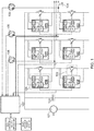
- FIG. 1 is a block diagram of an example power converter (in this case an inverter) including a health prognosis system i.e. a system for monitoring the health of the power converter.
- a DC source 101 is connected via a capacitor 102 to a series of insulated gate bipolar transistors (IGBTs) 103, which are connected to a load 104.
- IGBTs insulated gate bipolar transistors
- the IGBTs can be referred to as power converting devices.
- the IGBTs are switched such that the output current to the load is an AC current.
- each IGBT Connected to each IGBT is a gate driver 105, which includes an embedded health prognosis system.
- Each gate driver 105 includes a module for measuring: the gate charge Q G , rate of change of voltage across the IGBT d V d t , and rate of change of current d i d t .
- the gate driver 105 may also include an analogue to digital converter and/or digital to analogue converter, as well as a module for directly measuring the voltage across the collector and emitter of the IGBT when it is switched on: V CE ON .
- At least some of the outputs of the IGBTs are connected to current sensors 106, and both the current sensors and gate drivers can be connected to a digital processor 107. The output of this digital processor may be subjected to signal conditioning and data management. The health status of the IGBTs may therefore be determined.
- each power device i.e. IGBT
- IGBT power device
- a gate driver with the capabilities discussed above can be referred to as a gate driver with embedded prognosis capability (GDEPC).
- GDEPC can transmit the observed variation to a processing system such as the digital processor, which can allow the device health status to be determined and analysed.
- the device health status can be determined by a processor embedded in the gate driver.
- the digital processor either external or embedded, can intelligently manage the data acquisition from the GDEPCs and communicate with a converter system controller to enable the derivation of the system level health status and also a remaining useful lifetime (RUL) estimation for the system.
- RUL remaining useful lifetime
- the system level health indication and RUL estimation of the system can either be done in the digital processor connected to each converter or at a separate dedicated processor responsible for monitoring the health of the converter.
- This separate dedicated processor can derive the RUL and system health of the entire converter by considering the individual component health, RUL status, and expected usage profiles.
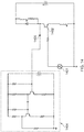
- FIG. 2 shows in more detail a gate driver with embedded prognostic capability (GDEPC).
- the GDEPC manages the switching time, isolation, and other basic functions needed to operate an IGBT 201 as well as measuring the electrical parameters needed to detect the ageing (i.e. deterioration in health) of the power module.
- the term 'ageing' can be considered to define a degradation process that leaves the device operating in an un-safe mode i.e. it is unhealthy.
- the GDEPC primarily detects the ageing of power modules due to temperature and power cycling, and does so by measuring one or more of the following parameters: the gate charge Q G , rate of change of voltage across the IGBT d V d t , and rate of change of current d i d t .
- a Miller capacitor 203 connected to a d V d t module 207, a gate resistor 202 connected to a gate driver with gate charge Q G measurement module 206, and a d i d t measurement module 205 connected to a Kelvin emitter 204.
- the Kelvin emitter 204 is connected in series with the emitter terminal of the IGBT 201.
- the rate of change of current, rate of change of voltage, and gate charge measurements require high bandwidth sensors. This would be expensive and difficult to implement as an integral part of the converter. Therefore measurement circuits may be implemented in the gate drive of each IGBT to measure each of these parameters. In addition to the three parameters discussed above, it is also possible to determine the peak overshoot voltage and peak overshoot or reverse recovery current from the circuits used to measure d V d t and d i d t respectively. Alternatively, as will be appreciated by one skilled in the art, separate circuits can be provided to directly measure the peak overshoot voltage and/or the peak overshoot or reverse recovery current.
- the derivation of the health status of the devices may have two components.
- the first monitors the abovementioned parameters to detect any significant change in the most recently measured parameters as compared to historically measured parameters.
- the second based upon the most recently measured parameters, specifies the current operating condition of the system.
- the health status of the device can be determined by observing the magnitude of the abovementioned parameters. For example the value of these observed parameters can be compared with pre-defined threshold values that indicate the health condition of the device.
- a look-up table can be provided in the GDEPC which enables the GDEPC to ascertain the health condition of the device. The data in the look-up table can be obtained by performing accelerated aging tests on representative examples of the device (e.g. IGBTs of the same or similar specification).
- a problem in the use of these parameters to indicate the health of power devices can be their dependency on the age of the device as well as the current operating conditions (such as junction temperature). Therefore in some circumstances unprocessed measurements of the parameters may not be suitable for prognostic indicators, and may require normalizing.
- an electro-thermal model is used in a processor embedded in the gate drive to normalise the parameters. In such examples, all the measured prognostic indicators can be normalised with respect to variation in temperature. It is also possible to normalise the parameters with respect to the device operating current as well.
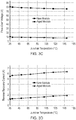
- Figures 3A-3D show the dependency of the parameters for both new/healthy and aged/unhealthy modules (i.e. components) on junction temperature. As can be seen in all of the plots, the rate of change of the respective parameter with temperature is approximately the same for both new and aged modules. For example, as is clear from Figure 3A , the rate of change of voltage decreases with increasing junction temperature for both old and new components. The same applied for Figures 3B - 3D and their respective parameters.
- the use of an embedded processor in the gate driver can enable the triggering of data capture which may facilitate data management.
- the sampling frequency i.e. the rate at which data capture is triggered
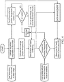
- the sampling frequency can be varied based upon the health status of the component, as shown in flow diagram in Figure 4 .
- 'x' represents the number of cycles that should have occurred before measurement is to take place.
- x can be varied in light of the comparison between the normalised measurements and the pre-defined thresholds.
- the case temperature and phase current of the device can be used to estimate the junction temperature using a compact thermal model. From the estimated junction temperature, a number of temperature cycles can be counted using a rain flow algorithm. When the temperature cycle counts reach a predetermined number of cycles 'x', the controller sends an enabling signal to trigger the collection of the various parameters. The measured parameters can then be normalised and compared with previously observed parameters. If any changes are detected a signal can be transmitted which is indicative of the health status of the device.
- the number of cycles that can be used for sampling the data can be linear or it can be changed considering the health status of the device to improve the accuracy of the RUL estimation. For example more samples can be taken when the device is near the end of its RUL.
- Figure 5 is a block schematic of a junction temperature estimation method. Any one of the three measured parameters can be taken as inputs together with or instead of the case temperature and used life. A look-up table can then be used to estimate the junction temperature, and the estimated value stored in memory.
- the three parameters are able to be used to estimate the health of a component due to their predicable behaviour with respect to the number of cycles (i.e. the age of the component).
- Figure 6 is a plot of the three parameters: rate of change of voltage, rate of change of current, and gate charge as a function of temperature cycle.
- the parameters show small changes. However once the temperature cycle value surpasses 20,000 cycles there are significant changes in comparison to the previously observed values and the observed values indicate that the device is no longer healthy.
- pre-selected threshold values are stored and used as health indicators and also to calculate the used life as well as the remaining useful life. It is also possible to use a particle filter to predict the remaining life by considering variations in the parameters towards pre-defined threshold values.
- Figure 7 is a similar plot but indicating the dependence of peak over voltage V PO and reverse recovery current I RR with respect to temperature cycle value.
- the three parameters in Figure 6 can be measured utilizing simple circuits which are embedded with the gate driver. In principle, only one or just two of the parameters can be measured, but a more accurate estimate of the health of the IGBT can be obtained by measuring all three.
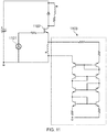
- FIG 8 shows a test circuit 803 suitable to measure the gate charge on an IGBT 802.
- the IGBT is controlled by voltage source 801.
- an approximately constant current (shown in Figure 9 ) is supplied to the gate of the IGBT from two switches s1, s2 and two current diodes.
- switch s1 is closed and s2 is open.
- switch s2 is closed and switch s1 opened.
- the gate charge at a particular gate voltage is the product of the gate charge with respect to the time required to achieve that particular gate voltage from an initial voltage value.
- the gate-emitter voltage V GE and the gate current i G are shown by the plots in Figure 9 .
- Figure 10 is a circuit which can be used to extract a value for the gate charge from the measured gate-emitter voltage under a constant gate current.
- the measured gate-emitter voltage 1003 is compared 1007 with an input voltage reference which is either an on state voltage 1001 or off state voltage 1002. In some examples this is assumed to be 15V for an on state, and -5V or 0V for an off state.
- the output of the comparator generates a logic pulse which enables an integrator 1007 to estimate the gate charge 1008 of the device.
- the rate of change of current can be estimated using the circuit shown in Figure 11 .
- a power device such as an IGBT
- the collector current will start rising and reach a steady state value in the immediate neighbourhood of the gate to the emitter junction.
- a minimum time is required for the device to spread the current conduction consistently through the conduction channel.
- the current can spread across the whole area of the junction which may surpass the transistor design limits. Due to the rate of increase in collector current, local hot spots can be formed close to the gate connection. These local hot spots can destroy the transistor. Therefore this rate of increase of current is an important factor for analysing the deterioration in health of an IGBT.
- the sub-circuit 1103 shown in Figure 11 is a current mirror connected across a sensing resistor parallel to the IGBT's 1102 Kelvin emitter, where the IGBT 1102 is controlled by voltage source 1101. If the IGBT 1102 is lacking a Kelvin emitter terminal, an emitter can be connected with a small inductance to ground in order to measure the rate of change of current.
- Figure 12 shows two waveforms: the collector current as measured in a simulation of the IGBT, and the collector current as measured in a simulation of the current mirror connected to the simulated IGBT. This plot shows that the error between the measured current using the oscilloscope and the current mirror is very small over the applicable regime (during the switch-on period). Therefore the current measured from the current mirror can be used as a representative value of the actual collector current through the IGBT over the applicable regime.
- Figure 13 is a circuit which can be used to estimate the rate of change of current 1310 from the current mirror output 1302.
- the input 1302 is compared 1306 to a reference value 1301 which in this case is the reference operating current limit 1301.
- the output of the comparator 1306 is a pulse with a modified pulse width which allows an integrator 1308 to estimate the value of the rate of change of current 1310.
- a peak detector 1309 can be used to estimate the reverse recovery current I rr of the device.
- the rate of change of voltage can be measured through the use of a sub-circuit 1404 as shown in Figure 14 .
- a forward voltage is applied across the collector and emitter of a transistor, the outer junction of the transistor is forward biased and the inner junction is reverse biased due to the space-charges exiting the depletion region. Therefore it behaves like a capacitance, as illustrated by Miller capacitor 1405, and induces a potential stress across the IGBT module.
- Figure 15 shows the results of a simulation which directly measured the rate of change of collector-emitter voltage as compared to the collector-emitter voltage measured from the external Miller capacitor 1405. This plot shows that over the relevant regime (switch-off) the rate of change of the voltage measured over the external Miller capacitor 1405 is very similar to the directly measured rate of change of collector-emitter voltage. Therefore the rate of change of voltage measured over the external Miller capacitor 1405 can be used as a representative value of the actual rate of change of collector-emitter voltage over the applicable regime.
- the rate of change of voltage can then be estimated using the circuit shown in Figure 16 , which takes as its inputs the measurement voltage from the Miller circuit 1602 and an input voltage reference 1601. The values are compared 1606 and the output is a pulse with a modified pulse width. This output can be used by an integrator 1608 to estimate the rate of change of voltage 1610. A peak detector 1609 can also be used to extract the off-state overshoot voltage ( V PO ) 1611 of the device.
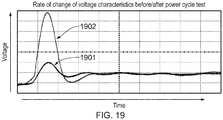
- Figure 17 to 19 show ageing test results that confirm the suitability of the three parameters for estimating aging.
- Figure 17 is a plot showing the change in gate charge characteristics before 1702 and after 1701 a power cycling test. As can be seen, whilst the gate voltage takes the same switching time to reach the operating voltage both before and after, the overall gate charge has increased after a power cycling tests.
- Figure 18 shows that the rate of change of current before 1802 and after 1801 a power cycling test are appreciably different. The results of the test is that the rate of change of current increases after being subjected to a power cycling test.
- Figure 19 shows that the rate of change of voltage before 1902 and after 1901 a power cycling test are appreciably different.
- the result of the test is that the rate of change of voltage decreases after being subjected to a power cycling test. From equation (3) it can be seen that the reduction of rate of change of voltage is the effect of decreasing the turn off delay time t doff . Asides from the rate of change of voltage, the peak overshoot voltage (highest value before reaching a steady state) also decreases.
- FIG 20 shows a schematic of an example propulsion system.
- a power supply 2001 in this example an AC supply, connects to a power device 2002 (e.g. of the type shown in Figure 1 ) which includes at least one IGBT.
- the power device 2002 provides an electrical supply to a propulsion component 2003 e.g. a motor, fuel pump etc.
- This propulsion component 2003 is functionally linked to a propulsion drive 2004 e.g. a propeller, gas-turbine engine etc.
- the invention as described above may provide the following advantages:
- the invention may be applicable in a number of industrial, automobile, and aero electric converter systems to monitor the health and life of the system.
- the converter systems can be, for example, DC/DC, DC/AC, or AC/DC converters.
- the converters can use different types of power modules, for example Si, SiC, GaN, etc.
- the health monitoring system can be expanded to include other component monitoring capabilities. For example the monitoring of capacitor and filter performance etc.
Landscapes
- Engineering & Computer Science (AREA)
- Physics & Mathematics (AREA)
- General Physics & Mathematics (AREA)
- Power Engineering (AREA)
- Microelectronics & Electronic Packaging (AREA)
- Power Conversion In General (AREA)
Claims (13)
- Verfahren zum Überwachen der Integrität eines elektronischen Halbleiter-Leistungsschalters (103; 201; 802; 1102; 1402) mit den Schritten zum:
Messen von einem oder mehreren Parametern, die aus der Gruppe ausgewählt werden, bestehend aus: einer Änderungsrate der Spannung

- Verfahren nach Anspruch 1, wobei der Schritt zum Schätzen der Integrität ein Vergleichen des oder der gemessenen Parameter mit einem oder mehreren jeweiligen vordefinierten Schwellenwerten des oder der Parameter enthält.
- Verfahren nach Anspruch 1 oder Anspruch 2, wobei:nur zwei oder alle drei Parameter in dem Messschritt gemessen werden; einer der gemessenen Parameter in dem Schritt zum Schätzen der Sperrschichttemperatur verwendet wird, um die Sperrschichttemperatur zu messen; undder oder jeder andere gemessene Parameter in dem Schritt zum Schätzen der Integrität normalisiert und zum Schätzen der Integrität des Schalters verwendet wird.
- Verfahren nach einem der vorhergehenden Ansprüche, wobei der Messschritt und der Schritt zum Schätzen der Integrität wiederholt mit einer Abtastfrequenz ausgeführt werden, und wobei die Abtastfrequenz eine Funktion der geschätzten Integrität des Schalters ist.
- Verfahren nach einem der vorhergehenden Ansprüche, wobei der oder die Parameter in dem Messschritt durch jeweils einen oder mehrere eingebettete Messschaltungen eines Gate-Treibers des Schalters gemessen werden.
- Energieumwandlungssystem, enthaltend:mindestens einen elektronischen Halbleiter-Leistungsschalter, wobei der Schalter (103) einen Gate-Treiber (105) hat; undeinen Prozessor (107), der mit dem Schalter verbunden ist;wobei der Gate-Treiber ein oder mehrere Parameter-Messmodule (205, 206, 207; 1103, 803 1404) zum Messen von einem oder mehreren jeweiligen Parametern hat, die aus der Gruppe ausgewählt werden, bestehend aus: einer Änderungsrate der Spannung


- Energieumwandlungssystem nach Anspruch 6, wobei der Prozessor in den Gate-Treiber eingebettet ist.
- Energieumwandlungssystem nach Anspruch 6 oder 7, wobei der Prozessor konfiguriert ist, um die Integrität des Schalters durch Vergleichen des oder der gemessenen Parameter mit einem oder mehreren jeweiligen vordefinierten Schwellenwerten des oder der Parameter zu schätzen.
- Energieumwandlungssystem nach einem der Ansprüche 6 bis 8, wobei die Parametermessmodule nur zwei oder alle drei Parameter messen; und
wobei der Prozessor konfiguriert ist, um die Sperrschichttemperatur unter Verwendung von einem der gemessenen Parameter zu schätzen; und die Integrität des Schalters unter Verwendung des oder jedes anderen normalisierten gemessenen Parameters zu schätzen. - Energieumwandlungssystem nach einem der Ansprüche 6 bis 9, wobei das oder die Parametermessmodule wiederholt den oder die Parameter mit einer Abtastfrequenz messen, die eine Funktion der geschätzten Integrität des Schalters ist, und der Prozessor konfiguriert ist, um die Integrität des Schalters mit der Abtastfrequenz zu schätzen.
- Energieumwandlungssystem nach einem der Ansprüche 6 bis 10, wobei das oder die Parametermessmodule jeweils eine oder mehrere eingebettete Messschaltungen (1103, 803 1404) des Gate-Treibers sind.
- Antriebssystem, enthaltend einen Elektroantrieb (2004). wobei der Elektroantrieb elektrisch mit dem Energieumwandlungssystem verbunden ist, wie in den Ansprüchen 6 bis 11 dargelegt.
- Gate-Treiber (105) für einen elektronischen Halbleiter-Leistungsschalter, wobei der Gate-Treiber geeignet ist, um in einem Energieumwandlungssystem installiert zu werden und aufweist:ein oder mehrere Parametermessmodule zum Messen von einem oder mehreren jeweiligen Parametern, die aus der Gruppe ausgewählt werden, bestehend aus: einer Änderungsrate der Spannung
 einen eingebetteten Prozessor, der konfiguriert ist, um eine Sperrschichttemperatur des Schalters zu schätzen und einen oder mehrere des oder der gemessenen Parameter in Bezug auf die geschätzte Sperrschichttemperatur zu normalisieren, um die Integrität des Schalters auf Grundlage des oder der gemessenen normalisierten Parameter zu schätzen.
Applications Claiming Priority (1)
| Application Number | Priority Date | Filing Date | Title |
|---|---|---|---|
| GBGB1609907.9A GB201609907D0 (en) | 2016-06-07 | 2016-06-07 | Method for estimating power system health |
Publications (2)
| Publication Number | Publication Date |
|---|---|
| EP3255443A1 EP3255443A1 (de) | 2017-12-13 |
| EP3255443B1 true EP3255443B1 (de) | 2018-08-22 |
Family
ID=56508175
Family Applications (1)
| Application Number | Title | Priority Date | Filing Date |
|---|---|---|---|
| EP17171253.2A Active EP3255443B1 (de) | 2016-06-07 | 2017-05-16 | Verfahren zur schätzung der integrität eines leistungssystems |
Country Status (3)
| Country | Link |
|---|---|
| US (1) | US10605854B2 (de) |
| EP (1) | EP3255443B1 (de) |
| GB (1) | GB201609907D0 (de) |
Cited By (1)
| Publication number | Priority date | Publication date | Assignee | Title |
|---|---|---|---|---|
| EP4417984A1 (de) | 2023-02-20 | 2024-08-21 | Abb Schweiz Ag | Verfahren zur vorhersage der lebensdauer einer leistungshalbleitervorrichtung |
Families Citing this family (26)
| Publication number | Priority date | Publication date | Assignee | Title |
|---|---|---|---|---|
| TWI769160B (zh) * | 2016-06-03 | 2022-07-01 | 美商英特矽爾美國有限公司 | 用以軟啟動大功率電荷泵的方法、電路,及電子系統 |
| CN106991221B (zh) * | 2017-03-24 | 2020-04-24 | 清华大学 | 一种基于igbt器件瞬态物理过程的分段折线建模方法 |
| US10942561B2 (en) | 2017-09-08 | 2021-03-09 | Texas Instruments Incorporated | Determination of one or more operating parameters for a switched-mode power supply |
| DE102017216644A1 (de) * | 2017-09-20 | 2019-03-21 | Siemens Aktiengesellschaft | Verfahren und Anordnung zum Erkennen von Teilentladungen bei einem elektrischen Betriebsmittel |
| JP6885862B2 (ja) * | 2017-12-28 | 2021-06-16 | ルネサスエレクトロニクス株式会社 | 電力変換装置 |
| US10845428B2 (en) | 2018-06-01 | 2020-11-24 | Infineon Technologies Ag | Method and circuit for detecting a loss of a bondwire in a power switch |
| CN109738773B (zh) * | 2018-06-19 | 2021-07-16 | 北京航空航天大学 | 一种非平稳工况下igbt模块寿命预测方法 |
| DE102019100594A1 (de) * | 2019-01-11 | 2020-07-16 | Semikron Elektronik Gmbh & Co. Kg | Leistungshalbleitereinrichtung mit einer Halbbrückenschaltung |
| CN111562477A (zh) * | 2019-01-29 | 2020-08-21 | 威海新佳电子有限公司 | 功率半导体器件的在线状态监测和故障判定系统 |
| JP7118019B2 (ja) * | 2019-02-05 | 2022-08-15 | 三菱電機株式会社 | 半導体モジュール、および半導体モジュールの寿命予測システム |
| EP3696558A1 (de) * | 2019-02-15 | 2020-08-19 | Siemens Aktiengesellschaft | Vorrichtung und verfahren zur automatischen prüfung eines schaltorgans |
| DE102019106976B4 (de) * | 2019-03-19 | 2021-04-22 | Argo-Hytos Group Ag | Filterdeckel, Filtereinrichtung, Filtersystem und Verfahren zur Berechnung der Reststandzeit eines Filterelements |
| US11397209B2 (en) * | 2019-06-18 | 2022-07-26 | Board Of Regents, The University Of Texas System | Methods of monitoring conditions associated with aging of silicon carbide power MOSFET devices in-situ, related circuits and computer program products |
| US12074530B2 (en) | 2019-11-06 | 2024-08-27 | General Electric Renovables España, S.L. | Systems and methods for controlling wind converters |
| CN111060798B (zh) * | 2019-12-18 | 2021-10-15 | 中国测试技术研究院流量研究所 | 一种mos管自动功率老化测试系统及测试方法 |
| DE102020103874B3 (de) | 2020-02-14 | 2021-06-10 | Infineon Technologies Ag | Verfahren und schaltung zum überprüfen der funktionsfähigkeit eines transistorbauelements |
| CN111398764B (zh) * | 2020-03-31 | 2022-06-14 | 中国电子产品可靠性与环境试验研究所((工业和信息化部电子第五研究所)(中国赛宝实验室)) | 功率管电压测试方法、装置和测试电路 |
| US11435395B2 (en) * | 2020-04-10 | 2022-09-06 | Semiconductor Components Industries, Llc | Circuit and method to detect defects in a power switching device |
| CN111398766B (zh) * | 2020-04-13 | 2021-05-28 | 武汉大学 | 一种igbt模块健康状态在线监测方法及系统 |
| CN112332646B (zh) * | 2020-10-22 | 2022-09-16 | 湖南国芯半导体科技有限公司 | 一种智能功率模块防过电压失效的方法及系统 |
| CN113406466B (zh) * | 2021-06-03 | 2024-05-17 | 合肥工业大学 | 一种igbt模块封装老化在线健康管理方法及系统 |
| US12379984B2 (en) | 2022-12-08 | 2025-08-05 | Toyota Motor Engineering & Manufacturing North America, Inc. | Remaining useful life determination for power electronic devices |
| GB2627448A (en) * | 2023-02-21 | 2024-08-28 | Rolls Royce Plc | Junction temperature estimation |
| CN117054726B (zh) * | 2023-06-30 | 2024-07-19 | 上海交通大学 | 一种有载分接开关切换过程恢复电压变化率计算方法 |
| EP4600670A1 (de) * | 2024-02-12 | 2025-08-13 | Mitsubishi Electric R&D Centre Europe B.V. | Elektronische schaltungsanordnung und verfahren zur bestimmung der verschlechterung eines spannungsgesteuerten leistungstransistors, zugehörige vorrichtung und computerprogramm |
| GB2641544A (en) * | 2024-06-05 | 2025-12-10 | Rolls Royce Deutschland Ltd & Co Kg | Monitoring health of a power converter |
Family Cites Families (12)
| Publication number | Priority date | Publication date | Assignee | Title |
|---|---|---|---|---|
| US7397264B2 (en) | 2005-08-22 | 2008-07-08 | Dolian Graphics, Inc. | Method for testing power MOSFET devices |
| US8103463B2 (en) | 2006-09-21 | 2012-01-24 | Impact Technologies, Llc | Systems and methods for predicting failure of electronic systems and assessing level of degradation and remaining useful life |
| US7826985B2 (en) * | 2008-05-02 | 2010-11-02 | Rockwell Automation Technologies, Inc. | Power module life estimation fatigue function |
| GB2497967B (en) | 2011-12-23 | 2018-02-21 | Reinhausen Maschf Scheubeck | Fault-tolerant control systems |
| EP2615467B1 (de) | 2012-01-11 | 2014-06-18 | ABB Research Ltd. | System und Verfahren zur Überwachung des Betriebszustands einer IGBT-Vorrichtung in Echtzeit |
| US8957723B2 (en) * | 2012-06-11 | 2015-02-17 | General Electric Company | Apparatus and method for power switch health monitoring |
| CN202903960U (zh) | 2012-07-12 | 2013-04-24 | 北京赛德高科铁道电气科技有限责任公司 | 一种机车变流功率模块igbt开关性能测试装置 |
| US9494657B2 (en) | 2012-10-16 | 2016-11-15 | University Of Utah Research Foundation | State of health estimation of power converters |
| EP3049779B1 (de) * | 2013-09-24 | 2017-11-15 | ABB Schweiz AG | Verfahren und vorrichtung zur bestimmung einer tatsächlichen übergangstemperatur einer igbt- vorrichtung |
| US20150193595A1 (en) * | 2014-01-08 | 2015-07-09 | IlnfoBionic, Inc. | Systems and methods for reporting patient health parameters |
| US9846182B2 (en) | 2014-05-30 | 2017-12-19 | Infineon Technologies Ag | High di/dt capacity measurement hardware |
| GB2532215A (en) | 2014-11-11 | 2016-05-18 | Reinhausen Maschf Scheubeck | Gate boost |
-
2016
- 2016-06-07 GB GBGB1609907.9A patent/GB201609907D0/en not_active Ceased
-
2017
- 2017-05-16 US US15/596,878 patent/US10605854B2/en active Active
- 2017-05-16 EP EP17171253.2A patent/EP3255443B1/de active Active
Cited By (2)
| Publication number | Priority date | Publication date | Assignee | Title |
|---|---|---|---|---|
| EP4417984A1 (de) | 2023-02-20 | 2024-08-21 | Abb Schweiz Ag | Verfahren zur vorhersage der lebensdauer einer leistungshalbleitervorrichtung |
| WO2024175541A1 (en) | 2023-02-20 | 2024-08-29 | Abb Schweiz Ag | A method for predicting a lifetime of a power semiconductor device |
Also Published As
| Publication number | Publication date |
|---|---|
| US20170350934A1 (en) | 2017-12-07 |
| GB201609907D0 (en) | 2016-07-20 |
| US10605854B2 (en) | 2020-03-31 |
| EP3255443A1 (de) | 2017-12-13 |
Similar Documents
| Publication | Publication Date | Title |
|---|---|---|
| EP3255443B1 (de) | Verfahren zur schätzung der integrität eines leistungssystems | |
| Givi et al. | A comprehensive monitoring system for online fault diagnosis and aging detection of non-isolated DC–DC converters’ components | |
| Pu et al. | A practical on-board SiC MOSFET condition monitoring technique for aging detection | |
| US11248966B2 (en) | Health monitoring and failure prognosis of power electronics devices | |
| US11169201B2 (en) | Diagnostic device and method to establish degradation state of electrical connection in power semiconductor device | |
| Eleffendi et al. | Evaluation of on-state voltage V CE (ON) and threshold voltage V th for real-time health monitoring of IGBT power modules | |
| Erturk et al. | A method for online ageing detection in SiC MOSFETs | |
| US11287465B2 (en) | Monitoring an operating condition of a transistor-based power converter | |
| Qiao et al. | Online junction temperature monitoring for SiC MOSFETs using turn-on delay time | |
| Patil et al. | Anomaly detection for IGBTs using Mahalanobis distance | |
| CN114355134B (zh) | 基于功率器件开通延迟时间的在线状态监测电路 | |
| Roy et al. | Aging detection and state of health estimation of live power semiconductor devices using SSTDR embedded PWM sequence | |
| Hanif et al. | Detection of gate oxide and channel degradation in SiC power MOSFETs using reflectometry | |
| Gonzalez et al. | Bias temperature instability and condition monitoring in SiC power MOSFETs | |
| Roy et al. | Live condition monitoring of switching devices using SSTDR embedded PWM sequence: A platform for intelligent gate-driver architecture | |
| Nasrin et al. | Characterization of aging process in power converters using spread spectrum time domain reflectometry | |
| WO2019198775A1 (ja) | 診断装置及び診断システム | |
| JP6714767B2 (ja) | 電力変換装置の診断回路、電力変換装置の診断システム | |
| KR101531018B1 (ko) | 전력반도체소자의 불량 예측 방법 | |
| Anderson et al. | Online algorithm for early stage fault detection in IGBT switches | |
| Krone et al. | Advanced condition monitoring system based on on-line semiconductor loss measurements | |
| Anderson et al. | An on-line fault diagnosis method for power electronic drives | |
| Roy et al. | State of health (SOH) estimation of multiple switching devices using a single intelligent gate driver module | |
| Nasrin et al. | Use of spread spectrum time domain reflectometry to estimate state of health of power converters | |
| O'Connor et al. | Near real-time incipient fault detection in IGBT switches |
Legal Events
| Date | Code | Title | Description |
|---|---|---|---|
| PUAI | Public reference made under article 153(3) epc to a published international application that has entered the european phase |
Free format text: ORIGINAL CODE: 0009012 |
|
| STAA | Information on the status of an ep patent application or granted ep patent |
Free format text: STATUS: THE APPLICATION HAS BEEN PUBLISHED |
|
| AK | Designated contracting states |
Kind code of ref document: A1 Designated state(s): AL AT BE BG CH CY CZ DE DK EE ES FI FR GB GR HR HU IE IS IT LI LT LU LV MC MK MT NL NO PL PT RO RS SE SI SK SM TR |
|
| AX | Request for extension of the european patent |
Extension state: BA ME |
|
| STAA | Information on the status of an ep patent application or granted ep patent |
Free format text: STATUS: REQUEST FOR EXAMINATION WAS MADE |
|
| GRAP | Despatch of communication of intention to grant a patent |
Free format text: ORIGINAL CODE: EPIDOSNIGR1 |
|
| STAA | Information on the status of an ep patent application or granted ep patent |
Free format text: STATUS: GRANT OF PATENT IS INTENDED |
|
| 17P | Request for examination filed |
Effective date: 20180514 |
|
| RBV | Designated contracting states (corrected) |
Designated state(s): AL AT BE BG CH CY CZ DE DK EE ES FI FR GB GR HR HU IE IS IT LI LT LU LV MC MK MT NL NO PL PT RO RS SE SI SK SM TR |
|
| GRAS | Grant fee paid |
Free format text: ORIGINAL CODE: EPIDOSNIGR3 |
|
| INTG | Intention to grant announced |
Effective date: 20180618 |
|
| GRAA | (expected) grant |
Free format text: ORIGINAL CODE: 0009210 |
|
| STAA | Information on the status of an ep patent application or granted ep patent |
Free format text: STATUS: THE PATENT HAS BEEN GRANTED |
|
| AK | Designated contracting states |
Kind code of ref document: B1 Designated state(s): AL AT BE BG CH CY CZ DE DK EE ES FI FR GB GR HR HU IE IS IT LI LT LU LV MC MK MT NL NO PL PT RO RS SE SI SK SM TR |
|
| REG | Reference to a national code |
Ref country code: GB Ref legal event code: FG4D |
|
| REG | Reference to a national code |
Ref country code: CH Ref legal event code: EP |
|
| REG | Reference to a national code |
Ref country code: AT Ref legal event code: REF Ref document number: 1033118 Country of ref document: AT Kind code of ref document: T Effective date: 20180915 |
|
| REG | Reference to a national code |
Ref country code: IE Ref legal event code: FG4D |
|
| REG | Reference to a national code |
Ref country code: DE Ref legal event code: R096 Ref document number: 602017000276 Country of ref document: DE |
|
| REG | Reference to a national code |
Ref country code: NL Ref legal event code: MP Effective date: 20180822 |
|
| REG | Reference to a national code |
Ref country code: LT Ref legal event code: MG4D |
|
| PG25 | Lapsed in a contracting state [announced via postgrant information from national office to epo] |
Ref country code: NL Free format text: LAPSE BECAUSE OF FAILURE TO SUBMIT A TRANSLATION OF THE DESCRIPTION OR TO PAY THE FEE WITHIN THE PRESCRIBED TIME-LIMIT Effective date: 20180822 Ref country code: BG Free format text: LAPSE BECAUSE OF FAILURE TO SUBMIT A TRANSLATION OF THE DESCRIPTION OR TO PAY THE FEE WITHIN THE PRESCRIBED TIME-LIMIT Effective date: 20181122 Ref country code: IS Free format text: LAPSE BECAUSE OF FAILURE TO SUBMIT A TRANSLATION OF THE DESCRIPTION OR TO PAY THE FEE WITHIN THE PRESCRIBED TIME-LIMIT Effective date: 20181222 Ref country code: LT Free format text: LAPSE BECAUSE OF FAILURE TO SUBMIT A TRANSLATION OF THE DESCRIPTION OR TO PAY THE FEE WITHIN THE PRESCRIBED TIME-LIMIT Effective date: 20180822 Ref country code: GR Free format text: LAPSE BECAUSE OF FAILURE TO SUBMIT A TRANSLATION OF THE DESCRIPTION OR TO PAY THE FEE WITHIN THE PRESCRIBED TIME-LIMIT Effective date: 20181123 Ref country code: RS Free format text: LAPSE BECAUSE OF FAILURE TO SUBMIT A TRANSLATION OF THE DESCRIPTION OR TO PAY THE FEE WITHIN THE PRESCRIBED TIME-LIMIT Effective date: 20180822 Ref country code: FI Free format text: LAPSE BECAUSE OF FAILURE TO SUBMIT A TRANSLATION OF THE DESCRIPTION OR TO PAY THE FEE WITHIN THE PRESCRIBED TIME-LIMIT Effective date: 20180822 Ref country code: NO Free format text: LAPSE BECAUSE OF FAILURE TO SUBMIT A TRANSLATION OF THE DESCRIPTION OR TO PAY THE FEE WITHIN THE PRESCRIBED TIME-LIMIT Effective date: 20181122 Ref country code: SE Free format text: LAPSE BECAUSE OF FAILURE TO SUBMIT A TRANSLATION OF THE DESCRIPTION OR TO PAY THE FEE WITHIN THE PRESCRIBED TIME-LIMIT Effective date: 20180822 |
|
| REG | Reference to a national code |
Ref country code: AT Ref legal event code: MK05 Ref document number: 1033118 Country of ref document: AT Kind code of ref document: T Effective date: 20180822 |
|
| PG25 | Lapsed in a contracting state [announced via postgrant information from national office to epo] |
Ref country code: AL Free format text: LAPSE BECAUSE OF FAILURE TO SUBMIT A TRANSLATION OF THE DESCRIPTION OR TO PAY THE FEE WITHIN THE PRESCRIBED TIME-LIMIT Effective date: 20180822 Ref country code: HR Free format text: LAPSE BECAUSE OF FAILURE TO SUBMIT A TRANSLATION OF THE DESCRIPTION OR TO PAY THE FEE WITHIN THE PRESCRIBED TIME-LIMIT Effective date: 20180822 Ref country code: LV Free format text: LAPSE BECAUSE OF FAILURE TO SUBMIT A TRANSLATION OF THE DESCRIPTION OR TO PAY THE FEE WITHIN THE PRESCRIBED TIME-LIMIT Effective date: 20180822 |
|
| PG25 | Lapsed in a contracting state [announced via postgrant information from national office to epo] |
Ref country code: AT Free format text: LAPSE BECAUSE OF FAILURE TO SUBMIT A TRANSLATION OF THE DESCRIPTION OR TO PAY THE FEE WITHIN THE PRESCRIBED TIME-LIMIT Effective date: 20180822 Ref country code: ES Free format text: LAPSE BECAUSE OF FAILURE TO SUBMIT A TRANSLATION OF THE DESCRIPTION OR TO PAY THE FEE WITHIN THE PRESCRIBED TIME-LIMIT Effective date: 20180822 Ref country code: PL Free format text: LAPSE BECAUSE OF FAILURE TO SUBMIT A TRANSLATION OF THE DESCRIPTION OR TO PAY THE FEE WITHIN THE PRESCRIBED TIME-LIMIT Effective date: 20180822 Ref country code: RO Free format text: LAPSE BECAUSE OF FAILURE TO SUBMIT A TRANSLATION OF THE DESCRIPTION OR TO PAY THE FEE WITHIN THE PRESCRIBED TIME-LIMIT Effective date: 20180822 Ref country code: IT Free format text: LAPSE BECAUSE OF FAILURE TO SUBMIT A TRANSLATION OF THE DESCRIPTION OR TO PAY THE FEE WITHIN THE PRESCRIBED TIME-LIMIT Effective date: 20180822 Ref country code: EE Free format text: LAPSE BECAUSE OF FAILURE TO SUBMIT A TRANSLATION OF THE DESCRIPTION OR TO PAY THE FEE WITHIN THE PRESCRIBED TIME-LIMIT Effective date: 20180822 Ref country code: CZ Free format text: LAPSE BECAUSE OF FAILURE TO SUBMIT A TRANSLATION OF THE DESCRIPTION OR TO PAY THE FEE WITHIN THE PRESCRIBED TIME-LIMIT Effective date: 20180822 |
|
| REG | Reference to a national code |
Ref country code: DE Ref legal event code: R097 Ref document number: 602017000276 Country of ref document: DE |
|
| PG25 | Lapsed in a contracting state [announced via postgrant information from national office to epo] |
Ref country code: SM Free format text: LAPSE BECAUSE OF FAILURE TO SUBMIT A TRANSLATION OF THE DESCRIPTION OR TO PAY THE FEE WITHIN THE PRESCRIBED TIME-LIMIT Effective date: 20180822 Ref country code: DK Free format text: LAPSE BECAUSE OF FAILURE TO SUBMIT A TRANSLATION OF THE DESCRIPTION OR TO PAY THE FEE WITHIN THE PRESCRIBED TIME-LIMIT Effective date: 20180822 Ref country code: SK Free format text: LAPSE BECAUSE OF FAILURE TO SUBMIT A TRANSLATION OF THE DESCRIPTION OR TO PAY THE FEE WITHIN THE PRESCRIBED TIME-LIMIT Effective date: 20180822 |
|
| PLBE | No opposition filed within time limit |
Free format text: ORIGINAL CODE: 0009261 |
|
| STAA | Information on the status of an ep patent application or granted ep patent |
Free format text: STATUS: NO OPPOSITION FILED WITHIN TIME LIMIT |
|
| 26N | No opposition filed |
Effective date: 20190523 |
|
| PG25 | Lapsed in a contracting state [announced via postgrant information from national office to epo] |
Ref country code: SI Free format text: LAPSE BECAUSE OF FAILURE TO SUBMIT A TRANSLATION OF THE DESCRIPTION OR TO PAY THE FEE WITHIN THE PRESCRIBED TIME-LIMIT Effective date: 20180822 |
|
| PG25 | Lapsed in a contracting state [announced via postgrant information from national office to epo] |
Ref country code: MC Free format text: LAPSE BECAUSE OF FAILURE TO SUBMIT A TRANSLATION OF THE DESCRIPTION OR TO PAY THE FEE WITHIN THE PRESCRIBED TIME-LIMIT Effective date: 20180822 |
|
| REG | Reference to a national code |
Ref country code: BE Ref legal event code: MM Effective date: 20190531 |
|
| PG25 | Lapsed in a contracting state [announced via postgrant information from national office to epo] |
Ref country code: LU Free format text: LAPSE BECAUSE OF NON-PAYMENT OF DUE FEES Effective date: 20190516 |
|
| PG25 | Lapsed in a contracting state [announced via postgrant information from national office to epo] |
Ref country code: TR Free format text: LAPSE BECAUSE OF FAILURE TO SUBMIT A TRANSLATION OF THE DESCRIPTION OR TO PAY THE FEE WITHIN THE PRESCRIBED TIME-LIMIT Effective date: 20180822 |
|
| PG25 | Lapsed in a contracting state [announced via postgrant information from national office to epo] |
Ref country code: IE Free format text: LAPSE BECAUSE OF NON-PAYMENT OF DUE FEES Effective date: 20190516 |
|
| PG25 | Lapsed in a contracting state [announced via postgrant information from national office to epo] |
Ref country code: BE Free format text: LAPSE BECAUSE OF NON-PAYMENT OF DUE FEES Effective date: 20190531 |
|
| PG25 | Lapsed in a contracting state [announced via postgrant information from national office to epo] |
Ref country code: PT Free format text: LAPSE BECAUSE OF FAILURE TO SUBMIT A TRANSLATION OF THE DESCRIPTION OR TO PAY THE FEE WITHIN THE PRESCRIBED TIME-LIMIT Effective date: 20181222 |
|
| PG25 | Lapsed in a contracting state [announced via postgrant information from national office to epo] |
Ref country code: LI Free format text: LAPSE BECAUSE OF NON-PAYMENT OF DUE FEES Effective date: 20200531 Ref country code: CH Free format text: LAPSE BECAUSE OF NON-PAYMENT OF DUE FEES Effective date: 20200531 |
|
| PG25 | Lapsed in a contracting state [announced via postgrant information from national office to epo] |
Ref country code: CY Free format text: LAPSE BECAUSE OF FAILURE TO SUBMIT A TRANSLATION OF THE DESCRIPTION OR TO PAY THE FEE WITHIN THE PRESCRIBED TIME-LIMIT Effective date: 20180822 |
|
| PG25 | Lapsed in a contracting state [announced via postgrant information from national office to epo] |
Ref country code: HU Free format text: LAPSE BECAUSE OF FAILURE TO SUBMIT A TRANSLATION OF THE DESCRIPTION OR TO PAY THE FEE WITHIN THE PRESCRIBED TIME-LIMIT; INVALID AB INITIO Effective date: 20170516 Ref country code: MT Free format text: LAPSE BECAUSE OF FAILURE TO SUBMIT A TRANSLATION OF THE DESCRIPTION OR TO PAY THE FEE WITHIN THE PRESCRIBED TIME-LIMIT Effective date: 20180822 |
|
| PG25 | Lapsed in a contracting state [announced via postgrant information from national office to epo] |
Ref country code: MK Free format text: LAPSE BECAUSE OF FAILURE TO SUBMIT A TRANSLATION OF THE DESCRIPTION OR TO PAY THE FEE WITHIN THE PRESCRIBED TIME-LIMIT Effective date: 20180822 |
|
| P01 | Opt-out of the competence of the unified patent court (upc) registered |
Effective date: 20230528 |
|
| PGFP | Annual fee paid to national office [announced via postgrant information from national office to epo] |
Ref country code: DE Payment date: 20250528 Year of fee payment: 9 |
|
| PGFP | Annual fee paid to national office [announced via postgrant information from national office to epo] |
Ref country code: FR Payment date: 20250526 Year of fee payment: 9 |
|
| PGFP | Annual fee paid to national office [announced via postgrant information from national office to epo] |
Ref country code: GB Payment date: 20260313 Year of fee payment: 10 |