EP3255668A1 - Puce - Google Patents
Puce Download PDFInfo
- Publication number
- EP3255668A1 EP3255668A1 EP15888779.4A EP15888779A EP3255668A1 EP 3255668 A1 EP3255668 A1 EP 3255668A1 EP 15888779 A EP15888779 A EP 15888779A EP 3255668 A1 EP3255668 A1 EP 3255668A1
- Authority
- EP
- European Patent Office
- Prior art keywords
- metal layer
- function modules
- redistribution structure
- carrier
- packaging function
- Prior art date
- Legal status (The legal status is an assumption and is not a legal conclusion. Google has not performed a legal analysis and makes no representation as to the accuracy of the status listed.)
- Ceased
Links
Images



Classifications
-
- H—ELECTRICITY
- H10—SEMICONDUCTOR DEVICES; ELECTRIC SOLID-STATE DEVICES NOT OTHERWISE PROVIDED FOR
- H10W—GENERIC PACKAGES, INTERCONNECTIONS, CONNECTORS OR OTHER CONSTRUCTIONAL DETAILS OF DEVICES COVERED BY CLASS H10
- H10W20/00—Interconnections in chips, wafers or substrates
- H10W20/40—Interconnections external to wafers or substrates, e.g. back-end-of-line [BEOL] metallisations or vias connecting to gate electrodes
- H10W20/41—Interconnections external to wafers or substrates, e.g. back-end-of-line [BEOL] metallisations or vias connecting to gate electrodes characterised by their conductive parts
- H10W20/43—Layouts of interconnections
-
- H—ELECTRICITY
- H10—SEMICONDUCTOR DEVICES; ELECTRIC SOLID-STATE DEVICES NOT OTHERWISE PROVIDED FOR
- H10W—GENERIC PACKAGES, INTERCONNECTIONS, CONNECTORS OR OTHER CONSTRUCTIONAL DETAILS OF DEVICES COVERED BY CLASS H10
- H10W20/00—Interconnections in chips, wafers or substrates
- H10W20/40—Interconnections external to wafers or substrates, e.g. back-end-of-line [BEOL] metallisations or vias connecting to gate electrodes
-
- H—ELECTRICITY
- H10—SEMICONDUCTOR DEVICES; ELECTRIC SOLID-STATE DEVICES NOT OTHERWISE PROVIDED FOR
- H10W—GENERIC PACKAGES, INTERCONNECTIONS, CONNECTORS OR OTHER CONSTRUCTIONAL DETAILS OF DEVICES COVERED BY CLASS H10
- H10W70/00—Package substrates; Interposers; Redistribution layers [RDL]
- H10W70/01—Manufacture or treatment
- H10W70/05—Manufacture or treatment of insulating or insulated package substrates, or of interposers, or of redistribution layers
- H10W70/08—Manufacture or treatment of insulating or insulated package substrates, or of interposers, or of redistribution layers by depositing layers on the chip or wafer, e.g. "chip-first" RDLs
- H10W70/09—Manufacture or treatment of insulating or insulated package substrates, or of interposers, or of redistribution layers by depositing layers on the chip or wafer, e.g. "chip-first" RDLs extending onto an encapsulation that laterally surrounds the chip or wafer, e.g. fan-out wafer level package [FOWLP] RDLs
-
- H—ELECTRICITY
- H10—SEMICONDUCTOR DEVICES; ELECTRIC SOLID-STATE DEVICES NOT OTHERWISE PROVIDED FOR
- H10W—GENERIC PACKAGES, INTERCONNECTIONS, CONNECTORS OR OTHER CONSTRUCTIONAL DETAILS OF DEVICES COVERED BY CLASS H10
- H10W70/00—Package substrates; Interposers; Redistribution layers [RDL]
- H10W70/60—Insulating or insulated package substrates; Interposers; Redistribution layers
-
- H—ELECTRICITY
- H10—SEMICONDUCTOR DEVICES; ELECTRIC SOLID-STATE DEVICES NOT OTHERWISE PROVIDED FOR
- H10W—GENERIC PACKAGES, INTERCONNECTIONS, CONNECTORS OR OTHER CONSTRUCTIONAL DETAILS OF DEVICES COVERED BY CLASS H10
- H10W70/00—Package substrates; Interposers; Redistribution layers [RDL]
- H10W70/60—Insulating or insulated package substrates; Interposers; Redistribution layers
- H10W70/611—Insulating or insulated package substrates; Interposers; Redistribution layers for connecting multiple chips together
-
- H—ELECTRICITY
- H10—SEMICONDUCTOR DEVICES; ELECTRIC SOLID-STATE DEVICES NOT OTHERWISE PROVIDED FOR
- H10W—GENERIC PACKAGES, INTERCONNECTIONS, CONNECTORS OR OTHER CONSTRUCTIONAL DETAILS OF DEVICES COVERED BY CLASS H10
- H10W70/00—Package substrates; Interposers; Redistribution layers [RDL]
- H10W70/60—Insulating or insulated package substrates; Interposers; Redistribution layers
- H10W70/611—Insulating or insulated package substrates; Interposers; Redistribution layers for connecting multiple chips together
- H10W70/614—Insulating or insulated package substrates; Interposers; Redistribution layers for connecting multiple chips together the multiple chips being integrally enclosed
-
- H—ELECTRICITY
- H10—SEMICONDUCTOR DEVICES; ELECTRIC SOLID-STATE DEVICES NOT OTHERWISE PROVIDED FOR
- H10W—GENERIC PACKAGES, INTERCONNECTIONS, CONNECTORS OR OTHER CONSTRUCTIONAL DETAILS OF DEVICES COVERED BY CLASS H10
- H10W70/00—Package substrates; Interposers; Redistribution layers [RDL]
- H10W70/60—Insulating or insulated package substrates; Interposers; Redistribution layers
- H10W70/611—Insulating or insulated package substrates; Interposers; Redistribution layers for connecting multiple chips together
- H10W70/616—Insulating or insulated package substrates; Interposers; Redistribution layers for connecting multiple chips together package substrates, interposers or redistribution layers combined with bridge chips
- H10W70/618—Insulating or insulated package substrates; Interposers; Redistribution layers for connecting multiple chips together package substrates, interposers or redistribution layers combined with bridge chips the bridge chips being embedded in the package substrates, interposers or redistribution layers
-
- H—ELECTRICITY
- H10—SEMICONDUCTOR DEVICES; ELECTRIC SOLID-STATE DEVICES NOT OTHERWISE PROVIDED FOR
- H10W—GENERIC PACKAGES, INTERCONNECTIONS, CONNECTORS OR OTHER CONSTRUCTIONAL DETAILS OF DEVICES COVERED BY CLASS H10
- H10W70/00—Package substrates; Interposers; Redistribution layers [RDL]
- H10W70/60—Insulating or insulated package substrates; Interposers; Redistribution layers
- H10W70/62—Insulating or insulated package substrates; Interposers; Redistribution layers characterised by their interconnections
- H10W70/63—Vias, e.g. via plugs
- H10W70/635—Through-vias
-
- H—ELECTRICITY
- H10—SEMICONDUCTOR DEVICES; ELECTRIC SOLID-STATE DEVICES NOT OTHERWISE PROVIDED FOR
- H10W—GENERIC PACKAGES, INTERCONNECTIONS, CONNECTORS OR OTHER CONSTRUCTIONAL DETAILS OF DEVICES COVERED BY CLASS H10
- H10W72/00—Interconnections or connectors in packages
-
- H—ELECTRICITY
- H10—SEMICONDUCTOR DEVICES; ELECTRIC SOLID-STATE DEVICES NOT OTHERWISE PROVIDED FOR
- H10W—GENERIC PACKAGES, INTERCONNECTIONS, CONNECTORS OR OTHER CONSTRUCTIONAL DETAILS OF DEVICES COVERED BY CLASS H10
- H10W72/00—Interconnections or connectors in packages
- H10W72/01—Manufacture or treatment
- H10W72/0198—Manufacture or treatment batch processes
-
- H—ELECTRICITY
- H10—SEMICONDUCTOR DEVICES; ELECTRIC SOLID-STATE DEVICES NOT OTHERWISE PROVIDED FOR
- H10W—GENERIC PACKAGES, INTERCONNECTIONS, CONNECTORS OR OTHER CONSTRUCTIONAL DETAILS OF DEVICES COVERED BY CLASS H10
- H10W72/00—Interconnections or connectors in packages
- H10W72/50—Bond wires
-
- H—ELECTRICITY
- H10—SEMICONDUCTOR DEVICES; ELECTRIC SOLID-STATE DEVICES NOT OTHERWISE PROVIDED FOR
- H10W—GENERIC PACKAGES, INTERCONNECTIONS, CONNECTORS OR OTHER CONSTRUCTIONAL DETAILS OF DEVICES COVERED BY CLASS H10
- H10W90/00—Package configurations
-
- H—ELECTRICITY
- H10—SEMICONDUCTOR DEVICES; ELECTRIC SOLID-STATE DEVICES NOT OTHERWISE PROVIDED FOR
- H10W—GENERIC PACKAGES, INTERCONNECTIONS, CONNECTORS OR OTHER CONSTRUCTIONAL DETAILS OF DEVICES COVERED BY CLASS H10
- H10W90/00—Package configurations
- H10W90/701—Package configurations characterised by the relative positions of pads or connectors relative to package parts
-
- H—ELECTRICITY
- H10—SEMICONDUCTOR DEVICES; ELECTRIC SOLID-STATE DEVICES NOT OTHERWISE PROVIDED FOR
- H10W—GENERIC PACKAGES, INTERCONNECTIONS, CONNECTORS OR OTHER CONSTRUCTIONAL DETAILS OF DEVICES COVERED BY CLASS H10
- H10W20/00—Interconnections in chips, wafers or substrates
- H10W20/40—Interconnections external to wafers or substrates, e.g. back-end-of-line [BEOL] metallisations or vias connecting to gate electrodes
- H10W20/45—Interconnections external to wafers or substrates, e.g. back-end-of-line [BEOL] metallisations or vias connecting to gate electrodes characterised by their insulating parts
- H10W20/48—Insulating materials thereof
-
- H—ELECTRICITY
- H10—SEMICONDUCTOR DEVICES; ELECTRIC SOLID-STATE DEVICES NOT OTHERWISE PROVIDED FOR
- H10W—GENERIC PACKAGES, INTERCONNECTIONS, CONNECTORS OR OTHER CONSTRUCTIONAL DETAILS OF DEVICES COVERED BY CLASS H10
- H10W40/00—Arrangements for thermal protection or thermal control
- H10W40/20—Arrangements for cooling
- H10W40/22—Arrangements for cooling characterised by their shape, e.g. having conical or cylindrical projections
-
- H—ELECTRICITY
- H10—SEMICONDUCTOR DEVICES; ELECTRIC SOLID-STATE DEVICES NOT OTHERWISE PROVIDED FOR
- H10W—GENERIC PACKAGES, INTERCONNECTIONS, CONNECTORS OR OTHER CONSTRUCTIONAL DETAILS OF DEVICES COVERED BY CLASS H10
- H10W72/00—Interconnections or connectors in packages
- H10W72/071—Connecting or disconnecting
- H10W72/072—Connecting or disconnecting of bump connectors
-
- H—ELECTRICITY
- H10—SEMICONDUCTOR DEVICES; ELECTRIC SOLID-STATE DEVICES NOT OTHERWISE PROVIDED FOR
- H10W—GENERIC PACKAGES, INTERCONNECTIONS, CONNECTORS OR OTHER CONSTRUCTIONAL DETAILS OF DEVICES COVERED BY CLASS H10
- H10W72/00—Interconnections or connectors in packages
- H10W72/071—Connecting or disconnecting
- H10W72/073—Connecting or disconnecting of die-attach connectors
-
- H—ELECTRICITY
- H10—SEMICONDUCTOR DEVICES; ELECTRIC SOLID-STATE DEVICES NOT OTHERWISE PROVIDED FOR
- H10W—GENERIC PACKAGES, INTERCONNECTIONS, CONNECTORS OR OTHER CONSTRUCTIONAL DETAILS OF DEVICES COVERED BY CLASS H10
- H10W72/00—Interconnections or connectors in packages
- H10W72/20—Bump connectors, e.g. solder bumps or copper pillars; Dummy bumps; Thermal bumps
- H10W72/241—Dispositions, e.g. layouts
-
- H—ELECTRICITY
- H10—SEMICONDUCTOR DEVICES; ELECTRIC SOLID-STATE DEVICES NOT OTHERWISE PROVIDED FOR
- H10W—GENERIC PACKAGES, INTERCONNECTIONS, CONNECTORS OR OTHER CONSTRUCTIONAL DETAILS OF DEVICES COVERED BY CLASS H10
- H10W72/00—Interconnections or connectors in packages
- H10W72/851—Dispositions of multiple connectors or interconnections
- H10W72/874—On different surfaces
-
- H—ELECTRICITY
- H10—SEMICONDUCTOR DEVICES; ELECTRIC SOLID-STATE DEVICES NOT OTHERWISE PROVIDED FOR
- H10W—GENERIC PACKAGES, INTERCONNECTIONS, CONNECTORS OR OTHER CONSTRUCTIONAL DETAILS OF DEVICES COVERED BY CLASS H10
- H10W72/00—Interconnections or connectors in packages
- H10W72/90—Bond pads, in general
- H10W72/941—Dispositions of bond pads
- H10W72/9413—Dispositions of bond pads on encapsulations
-
- H—ELECTRICITY
- H10—SEMICONDUCTOR DEVICES; ELECTRIC SOLID-STATE DEVICES NOT OTHERWISE PROVIDED FOR
- H10W—GENERIC PACKAGES, INTERCONNECTIONS, CONNECTORS OR OTHER CONSTRUCTIONAL DETAILS OF DEVICES COVERED BY CLASS H10
- H10W74/00—Encapsulations, e.g. protective coatings
- H10W74/01—Manufacture or treatment
- H10W74/012—Manufacture or treatment of encapsulations on active surfaces of flip-chip devices, e.g. forming underfills
-
- H—ELECTRICITY
- H10—SEMICONDUCTOR DEVICES; ELECTRIC SOLID-STATE DEVICES NOT OTHERWISE PROVIDED FOR
- H10W—GENERIC PACKAGES, INTERCONNECTIONS, CONNECTORS OR OTHER CONSTRUCTIONAL DETAILS OF DEVICES COVERED BY CLASS H10
- H10W74/00—Encapsulations, e.g. protective coatings
- H10W74/01—Manufacture or treatment
- H10W74/019—Manufacture or treatment using temporary auxiliary substrates
-
- H—ELECTRICITY
- H10—SEMICONDUCTOR DEVICES; ELECTRIC SOLID-STATE DEVICES NOT OTHERWISE PROVIDED FOR
- H10W—GENERIC PACKAGES, INTERCONNECTIONS, CONNECTORS OR OTHER CONSTRUCTIONAL DETAILS OF DEVICES COVERED BY CLASS H10
- H10W74/00—Encapsulations, e.g. protective coatings
- H10W74/10—Encapsulations, e.g. protective coatings characterised by their shape or disposition
- H10W74/131—Encapsulations, e.g. protective coatings characterised by their shape or disposition the semiconductor body being only partially enclosed
- H10W74/142—Encapsulations, e.g. protective coatings characterised by their shape or disposition the semiconductor body being only partially enclosed the encapsulations exposing the passive side of the semiconductor body
-
- H—ELECTRICITY
- H10—SEMICONDUCTOR DEVICES; ELECTRIC SOLID-STATE DEVICES NOT OTHERWISE PROVIDED FOR
- H10W—GENERIC PACKAGES, INTERCONNECTIONS, CONNECTORS OR OTHER CONSTRUCTIONAL DETAILS OF DEVICES COVERED BY CLASS H10
- H10W74/00—Encapsulations, e.g. protective coatings
- H10W74/10—Encapsulations, e.g. protective coatings characterised by their shape or disposition
- H10W74/15—Encapsulations, e.g. protective coatings characterised by their shape or disposition on active surfaces of flip-chip devices, e.g. underfills
-
- H—ELECTRICITY
- H10—SEMICONDUCTOR DEVICES; ELECTRIC SOLID-STATE DEVICES NOT OTHERWISE PROVIDED FOR
- H10W—GENERIC PACKAGES, INTERCONNECTIONS, CONNECTORS OR OTHER CONSTRUCTIONAL DETAILS OF DEVICES COVERED BY CLASS H10
- H10W90/00—Package configurations
- H10W90/10—Configurations of laterally-adjacent chips
-
- H—ELECTRICITY
- H10—SEMICONDUCTOR DEVICES; ELECTRIC SOLID-STATE DEVICES NOT OTHERWISE PROVIDED FOR
- H10W—GENERIC PACKAGES, INTERCONNECTIONS, CONNECTORS OR OTHER CONSTRUCTIONAL DETAILS OF DEVICES COVERED BY CLASS H10
- H10W90/00—Package configurations
- H10W90/20—Configurations of stacked chips
-
- H—ELECTRICITY
- H10—SEMICONDUCTOR DEVICES; ELECTRIC SOLID-STATE DEVICES NOT OTHERWISE PROVIDED FOR
- H10W—GENERIC PACKAGES, INTERCONNECTIONS, CONNECTORS OR OTHER CONSTRUCTIONAL DETAILS OF DEVICES COVERED BY CLASS H10
- H10W90/00—Package configurations
- H10W90/701—Package configurations characterised by the relative positions of pads or connectors relative to package parts
- H10W90/721—Package configurations characterised by the relative positions of pads or connectors relative to package parts of bump connectors
- H10W90/722—Package configurations characterised by the relative positions of pads or connectors relative to package parts of bump connectors between stacked chips
-
- H—ELECTRICITY
- H10—SEMICONDUCTOR DEVICES; ELECTRIC SOLID-STATE DEVICES NOT OTHERWISE PROVIDED FOR
- H10W—GENERIC PACKAGES, INTERCONNECTIONS, CONNECTORS OR OTHER CONSTRUCTIONAL DETAILS OF DEVICES COVERED BY CLASS H10
- H10W90/00—Package configurations
- H10W90/701—Package configurations characterised by the relative positions of pads or connectors relative to package parts
- H10W90/721—Package configurations characterised by the relative positions of pads or connectors relative to package parts of bump connectors
- H10W90/724—Package configurations characterised by the relative positions of pads or connectors relative to package parts of bump connectors between a chip and a stacked insulating package substrate, interposer or RDL
-
- H—ELECTRICITY
- H10—SEMICONDUCTOR DEVICES; ELECTRIC SOLID-STATE DEVICES NOT OTHERWISE PROVIDED FOR
- H10W—GENERIC PACKAGES, INTERCONNECTIONS, CONNECTORS OR OTHER CONSTRUCTIONAL DETAILS OF DEVICES COVERED BY CLASS H10
- H10W90/00—Package configurations
- H10W90/701—Package configurations characterised by the relative positions of pads or connectors relative to package parts
- H10W90/731—Package configurations characterised by the relative positions of pads or connectors relative to package parts of die-attach connectors
- H10W90/734—Package configurations characterised by the relative positions of pads or connectors relative to package parts of die-attach connectors between a chip and a stacked insulating package substrate, interposer or RDL
-
- H—ELECTRICITY
- H10—SEMICONDUCTOR DEVICES; ELECTRIC SOLID-STATE DEVICES NOT OTHERWISE PROVIDED FOR
- H10W—GENERIC PACKAGES, INTERCONNECTIONS, CONNECTORS OR OTHER CONSTRUCTIONAL DETAILS OF DEVICES COVERED BY CLASS H10
- H10W90/00—Package configurations
- H10W90/701—Package configurations characterised by the relative positions of pads or connectors relative to package parts
- H10W90/731—Package configurations characterised by the relative positions of pads or connectors relative to package parts of die-attach connectors
- H10W90/736—Package configurations characterised by the relative positions of pads or connectors relative to package parts of die-attach connectors between a chip and a stacked lead frame, conducting package substrate or heat sink
Definitions
- Embodiments of the present invention relate to chip technologies, and in particular, to a chip in which multiple packaging function modules are packaged side by side.
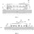
- a carrier 11 of a chip 100 carriers a wafer-level packaging (Water-Level Packaging, hereinafter referred to as WLP) 18.
- WLP 18 includes a die 12, a colloid 14 wrapped around the die 12, and a redistribution layer 15 formed on surfaces of the die 12 and the colloid 14.
- Bumps 17 are disposed at a bottom of the redistribution layer 15. The redistribution layer 15 and the bumps 17 form a signal path between the die 12 and the carrier 11.
- the chip 100 further includes a WLP 28 carried on a top of the WLP 18. Similar to the WLP 18, the WLP 28 includes a die 22, a colloid 24, a redistribution layer 25, and bumps 27. A redistribution layer 19 is disposed on the top of the WLP 18, a vertical interconnect path (Vertical Interconnect System) 13 is disposed in the colloid 14 of the WLP 18. The redistribution layer 25 and the bumps 27 that are of the WLP 28. A signal path is established between the WLP 28 and the WLP 18 by using a metal layer in the redistribution layer 25, the bumps 27, a metal layer in the redistribution layer 19 of the WLP 18, a through silicon via 13, and the redistribution layer 15 of the WLP 18.
- a metal layer in the redistribution layer 25 the bumps 27, a metal layer in the redistribution layer 19 of the WLP 18, a through silicon via 13, and the redistribution layer 15 of the WLP 18.
- a length of a signal path between two dies can be effectively shortened by means of superposition of two WLPs, but this also causes a new problem.
- superposition of the two WLPs causes a relatively severe dissipation problem;
- a process of a through silicon via is relatively difficult, which causes relatively high process costs.
- embodiments of the present invention provide a chip that can implement short-distance interconnection between dies but does not cause a dissipation problem.
- a first aspect of the embodiments of the present invention provides a chip, including a carrier, a redistribution structure, and multiple packaging function modules, where the multiple packaging function modules each have at least a part wrapped by a colloid, and are fastened to the redistribution structure side by side; the redistribution structure is fastened to the carrier, and the redistribution structure includes one or more redistribution metal layers; the redistribution metal layer communicatively connects the multiple packaging function modules and the carrier; and the redistribution structure further includes one or more interconnect metal layers, and the interconnect metal layer is communicatively connected to at least two packaging function modules so as to provide a signal path between the at least two packaging function modules.
- a main body of the redistribution structure is made of an insulation material, and the interconnect metal layer and the redistribution metal layer are mutually independent in the main body.
- pins are disposed on the multiple packaging function modules, and the pins are arranged between the packaging function modules and the redistribution structure, and are electrically connected to the redistribution metal layer or the interconnect metal layer.
- a bump array is disposed on the main body of the redistribution structure, and the bump array is electrically connected to the carrier and the redistribution metal layer.
- underfill is filled between the redistribution structure and the carrier, into a gap of the bump array, and around the bump array.
- a pad or a connector is disposed at a bottom of the carrier.
- sides that are of the multiple packaging function modules and deviate from the carrier are not wrapped by the colloid.
- surfaces of the sides that are of the multiple packaging function modules and deviate from the carrier are coated with thermal adhesives; and the chip further includes a heat sink, where the heat sink is attached to the surfaces of the sides that are of the multiple packaging function modules and deviate from the carrier.
- the heat sink includes a first part that is attached to tops of the multiple packaging function modules and a second part that surrounds the multiple packaging function modules and is fastened to a surface of the carrier by an adhesive.
- the chip further includes a ring heat sink, and the ring heat sink is disposed around the packaging function module, and is fastened to the carrier by an adhesive.
- the interconnect metal layer includes a first interconnect metal layer and a second interconnect metal layer, where a part of the first interconnect metal layer and a part of the second interconnect metal layer are mutually parallel; a reference metal layer is disposed between the parallel parts of the first interconnect metal layer and the second interconnect metal layer; and the reference metal layer is insulated from another metal layer in the redistribution structure.
- the packaging function module may be any one of the following: a die, stack dies, and a packaged chip.
- two packaging function modules are placed on a carrier side by side, and a signal path between the two packaging function modules is established by using a redistribution structure. Therefore, there is no dissipation problem caused by superposition; in addition, it can be effectively ensured that a length of the signal path between the packaging function modules is not excessively long.
- the present invention provides a chip of a new form.
- multiple dies Die are packaged on a surface of a carrier of the chip side by side, and a data path between the dies is directly established in a redistribution structure.
- a length of the data path between the dies can be effectively shortened; on the other hand, because there is no mutual impact between stacked chips, a better dissipation effect can be obtained.
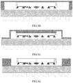
- FIG. 2 is a schematic diagram of a chip 200 according to a first embodiment of the present invention.
- the chip 200 includes a carrier 220, a redistribution structure 240, and multiple dies 260.
- the multiple dies mean two or more than two dies; for example, the chip shown in FIG. 1 includes two dies.
- the multiple dies 260 are fastened to a top of the redistribution structure 240 side by side, and the redistribution structure 240 is fastened to a top of the carrier 220.
- multiple dies packaged in one chip may be homogeneous chips, or may be heterogeneous chips.
- an analog die and a digital die may be packaged together, or dies produced by using different wafer process nodes may be packaged together, or dies with different functions may be packaged together.
- at least two dies 260 are wrapped by a colloid 262, and are fastened to the top of the redistribution structure 240 side by side.
- the redistribution structure 240 shown in FIG. 1 is a rectangle structure, and the top of the redistribution structure 240 is flat.
- the redistribution structure 240 may have an irregular shape, so that a height difference may exist on the top that is used to fasten the dies 260.
- that at least two dies 260 are fastened to the top of the redistribution structure 240 side by side does not mean that the dies 260 need to be disposed in a parallel manner, but merely means that at least two dies in the chip do not have a superposition relationship with each other, but are "equally" fastened to a surface of the redistribution structure 240.
- a main body of the redistribution structure 240 is made of an insulation material, and one or more redistribution metal layers 242 are inserted into the redistribution structure 240 or on the surface of the redistribution structure 240.
- the redistribution metal layers 242 are arranged layer by layer as one or more tree structures, and adjacent layers are electrically connected by using a copper plated via 250.
- a redistribution metal layer located on the top of the redistribution structure 240 is attached to a signal pin of the die 260.
- a bump array 245 is disposed at a bottom of the redistribution structure 240, so as to fasten the redistribution structure 240 to the carrier 220 in a tin soldering manner, and form a signal path between the die 260 and the carrier 220.
- the multiple redistribution metal layers 242 form multiple tree structures, and each tree structure is formed by multiple redistribution metal layers 242 and copper plated vias between the redistribution metal layers. These tree structures are not connected to each other inside the redistribution structure 240, and they each are connected to a signal pin of a corresponding die and a bump at the bottom of the redistribution structure 240, so as to form different signal paths inside the redistribution structure.
- underfill (Underfill) 262 may be filled between the redistribution structure 240 and the carrier, which helps alleviate stress on a solder ball, and improve packaging reliability.
- the redistribution structure 240 further includes one or more interconnect metal layers 244.
- the interconnect metal layer 244 and the redistribution metal layer 242 are mutually independent in the redistribution structure 240, that is, the interconnect metal layer and the redistribution metal layer are not connected to each other in the redistribution structure 240.
- the interconnect metal layer is not connected to a bump at the bottom of the redistribution structure 240 either. Any one of the interconnect metal layers 244 is electrically connected in a direct or indirect manner to pins of two different dies 260, so as to establish a signal path between the two dies.
- the dies 260 are disposed on the redistribution structure 240 side by side, which avoids a dissipation problem caused by superposition of the dies.
- data communication is performed between the dies directly by using the redistribution structure 240. This process is simple, and the design complexity is low, thereby effectively reducing process costs.
- the interconnect metal layer 244 includes a first interconnect metal layer 2442 and a second interconnect metal layer 2444 that are used to connect different pins of two dies.
- a part of the first interconnect metal layer 2442 and a part of the second interconnect metal layer 2444 approach to each other and are mutually parallel in the redistribution structure 240. In this way, signal crosstalk may occur between the first interconnect metal layer 2442 and the second interconnect metal layer 244, which affects signal transmission quality.
- a reference metal layer 2446 parallel to the two interconnect metal layers may be disposed inside the redistribution structure 240 and between the first interconnect metal layer 2442 and the second interconnect metal layer 2444, where the reference metal layer 2446 is surrounded by a medium layer of the redistribution structure, and the reference metal layer is insulated from another metal layer in the redistribution structure.
- a spacing between the dies affects performance of high density interconnection between the dies.
- the spacing between the dies is shortened as much as possible, for example, to below 50um, in a case in which the shortening is allowed.
- Step 3 Form a colloid in a molding manner to wrap the dies.
- a side that is of the die and corresponds to the redistribution structure needs to be made exposed by using a particular process processing method; for example, by using a grinding method, or, a corresponding position of the die is covered by a temporary carrier in a molding process, and the carrier is directly removed after the wrapping is completed.
- Step 4 Make, by using a redistribution process, a redistribution structure on a side that is of the die and corresponds to the redistribution structure.
- a medium of the main body of the redistribution structure may be formed by an organic medium that is insulated and is photo imageable upon exposure, such as a polyimide (Polyimide, hereinafter referred to as PI), poly-p-phenylenebenzobisthiazole (Poly-p-phenylenebenzobisthiazole, hereinafter referred to as PBO), or an epoxy based polymer (Epoxy Based Polymer).
- PI polyimide
- PBO poly-p-phenylenebenzobisthiazole
- Epoxy Based Polymer epoxy based polymer
- the redistribution metal layer and the interconnect metal layer may be made on the basis of the medium of the main body by using a process such as spluttering and plating, where a used material may be copper.
- a minimum line width and a line distance of the metal layer may respectively be: the line width is from 2um to 1um or shorter; the line distance is from 2um to 1um or shorter.
- a copper plated via may be made on the medium of the main body, so as to implement interconnection between different redistribution metal layers, where diameters of a via (Via) and a via land (Via Land) of the copper plated via may respectively reach 5um and 10um or shorter.
- the redistribution structure may be attached to a base board in a manner of hot air reflow (Mass Reflow), thermo compression bonding (Thermo Compression Bonding), or the like. Bottom underfill may be applied between the redistribution structure and the base board as required, to alleviate stress on a bump of the redistribution structure, so as to improve packaging reliability.
- the base board may be a multilayer base board, and inter-layer signal intercommunication is implemented in a manner of, for example, laser drilling Laser Drill or mechanical drilling Mechanical Drill and then copper plating.
- a pad is disposed at the bottom of the base board, so as to joint a PCB by using a solder ball (Solder Ball).
- solder Ball solder ball
- the bottom of the base board may be jointed to the PCB by using a pluggable connector (Socket).
- a multilayer base board can significantly increase a wiring resource used for packaging; in addition, a larger quantity of pins can be implemented by using a base board with a relatively large size specification, which can improve power integrity of packaging, and meanwhile can further greatly improve board-level reliability of packaging.
- multiple redistribution metal layers in a redistribution structure are utilized in the present invention, so that a requirement for reducing a quantity of layers of a base board can be met, thereby reducing packaging costs.
- the die except for a side close to the redistribution structure may be wrapped by the colloid.
- exposure processing such as grinding (Grinding) may be performed on a side that is of the die and away from the redistribution structure, so as to expose the side that is of the die and away from the redistribution structure, thereby improving dissipation efficiency, specifically as shown in FIG. 4 .
- a carrier may certainly be used to prevent this side of the die from being covered by the colloid when the die is being wrapped.
- a surface of the side that is of the die and away from the redistribution structure may be coated with a thermal adhesive, and then a heat sink 30 is attached.
- the heat sink shown in FIG. 5 is in a cap structure, the heat sink is globally bent and end segments are attached to a carrier 220. According to the heat sink of such a shape, on the one hand, heat dissipation of the die can be promoted; on the other hand, all dies are wrapped together, which is used as a further position limit, thereby effectively improving stability of a packaging structure.
- a shape of the heat sink may be in other various forms. For example, a heat sink shown in FIG.
- FIG. 6a is a forged unibody heat sink; a heat sink shown in FIG. 6b is a two-piece heat sink combined by at least two parts of dissipation metal sheets by using a post-processing mean.
- FIG. 6c a part attached to the die is blocked up based on the heat sink in FIG. 6a or FIG. 6b by using a boss.
- a ring heat sink may further be used.
- a layer that is of the die and away from the redistribution structure still does not need to be wrapped by the colloid, and the ring heat sink is arranged around the die and is fastened to the carrier by an adhesive.
- an external heat dissipator may be attached to the exposed side of the die and a top side of the ring heat sink, so as to obtain a better dissipation effect.
- FIG. 7 is a schematic diagram of a chip of another type based on the packaging structure in the embodiments of the present invention.
- the chip 500 includes a die 560 and stack dies 580 that are carried on a redistribution structure 400.
- a function module packaged in the chip in this embodiment of the present invention may be any combination of various types of function modules, such as a die and stack dies, a die and a chip that has been packaged once, or stack dies and a chip that has been packaged once.
- a quantity of function modules packaged in the chip may also be adjusted as required, and is not limited only to that merely two function modules (dies) are packaged side by side in the foregoing embodiments.
Landscapes
- Structures Or Materials For Encapsulating Or Coating Semiconductor Devices Or Solid State Devices (AREA)
- Cooling Or The Like Of Semiconductors Or Solid State Devices (AREA)
- Physics & Mathematics (AREA)
- Geometry (AREA)
Applications Claiming Priority (1)
| Application Number | Priority Date | Filing Date | Title |
|---|---|---|---|
| PCT/CN2015/076562 WO2016165074A1 (fr) | 2015-04-14 | 2015-04-14 | Puce |
Publications (2)
| Publication Number | Publication Date |
|---|---|
| EP3255668A1 true EP3255668A1 (fr) | 2017-12-13 |
| EP3255668A4 EP3255668A4 (fr) | 2018-07-11 |
Family
ID=57125607
Family Applications (1)
| Application Number | Title | Priority Date | Filing Date |
|---|---|---|---|
| EP15888779.4A Ceased EP3255668A4 (fr) | 2015-04-14 | 2015-04-14 | Puce |
Country Status (6)
| Country | Link |
|---|---|
| US (1) | US10475741B2 (fr) |
| EP (1) | EP3255668A4 (fr) |
| KR (1) | KR102008854B1 (fr) |
| CN (1) | CN108140632B (fr) |
| BR (1) | BR112017018820A2 (fr) |
| WO (1) | WO2016165074A1 (fr) |
Cited By (1)
| Publication number | Priority date | Publication date | Assignee | Title |
|---|---|---|---|---|
| US10490506B2 (en) | 2016-12-30 | 2019-11-26 | Huawei Technologies Co., Ltd. | Packaged chip and signal transmission method based on packaged chip |
Families Citing this family (7)
| Publication number | Priority date | Publication date | Assignee | Title |
|---|---|---|---|---|
| US11101209B2 (en) | 2017-09-29 | 2021-08-24 | Taiwan Semiconductor Manufacturing Company, Ltd. | Redistribution structures in semiconductor packages and methods of forming same |
| DE102018119298B4 (de) | 2017-09-29 | 2024-05-29 | Taiwan Semiconductor Manufacturing Co., Ltd. | Halbleiter-Packages |
| US12424515B2 (en) * | 2018-11-28 | 2025-09-23 | Taiwan Semiconductor Manufacturing Co., Ltd. | SOIC chip architecture |
| CN115066746A (zh) * | 2020-02-12 | 2022-09-16 | 华为技术有限公司 | 封装结构及其制备方法和电子设备 |
| US11908758B2 (en) | 2020-12-29 | 2024-02-20 | Samsung Electronics Co., Ltd. | Semiconductor package including dual stiffener |
| CN112802764B (zh) * | 2020-12-31 | 2024-03-26 | 上海易卜半导体有限公司 | 封装件及其形成方法 |
| CN117080179A (zh) * | 2023-08-21 | 2023-11-17 | 颀中科技(苏州)有限公司 | 散热贴贴附方法、封装方法、封装结构及贴附装置 |
Family Cites Families (60)
| Publication number | Priority date | Publication date | Assignee | Title |
|---|---|---|---|---|
| US5866952A (en) * | 1995-11-30 | 1999-02-02 | Lockheed Martin Corporation | High density interconnected circuit module with a compliant layer as part of a stress-reducing molded substrate |
| SG104293A1 (en) * | 2002-01-09 | 2004-06-21 | Micron Technology Inc | Elimination of rdl using tape base flip chip on flex for die stacking |
| DE10250538B4 (de) * | 2002-10-29 | 2008-02-21 | Infineon Technologies Ag | Elektronisches Bauteil als Multichipmodul und Verfahren zu dessen Herstellung |
| CN2591772Y (zh) * | 2002-12-26 | 2003-12-10 | 威盛电子股份有限公司 | 芯片封装结构 |
| JP4413174B2 (ja) * | 2004-09-01 | 2010-02-10 | 三洋電機株式会社 | アンテナ一体型回路装置 |
| US7326592B2 (en) * | 2005-04-04 | 2008-02-05 | Infineon Technologies Ag | Stacked die package |
| JP4072697B2 (ja) * | 2006-05-02 | 2008-04-09 | セイコーエプソン株式会社 | 半導体装置 |
| US7910385B2 (en) * | 2006-05-12 | 2011-03-22 | Micron Technology, Inc. | Method of fabricating microelectronic devices |
| US7535110B2 (en) * | 2006-06-15 | 2009-05-19 | Marvell World Trade Ltd. | Stack die packages |
| US7863090B2 (en) * | 2007-06-25 | 2011-01-04 | Epic Technologies, Inc. | Packaged electronic modules and fabrication methods thereof implementing a cell phone or other electronic system |
| US20090035895A1 (en) | 2007-07-30 | 2009-02-05 | Advanced Semiconductor Engineering, Inc. | Chip package and chip packaging process thereof |
| US7767496B2 (en) * | 2007-12-14 | 2010-08-03 | Stats Chippac, Ltd. | Semiconductor device and method of forming interconnect structure for encapsulated die having pre-applied protective layer |
| US8120186B2 (en) * | 2008-02-15 | 2012-02-21 | Qimonda Ag | Integrated circuit and method |
| CN100580918C (zh) * | 2008-03-05 | 2010-01-13 | 日月光半导体制造股份有限公司 | 可降低封装应力的封装构造 |
| KR101501739B1 (ko) | 2008-03-21 | 2015-03-11 | 삼성전자주식회사 | 반도체 패키지 제조 방법 |
| TWI362732B (en) * | 2008-04-07 | 2012-04-21 | Nanya Technology Corp | Multi-chip stack package |
| US7838975B2 (en) * | 2008-05-27 | 2010-11-23 | Mediatek Inc. | Flip-chip package with fan-out WLCSP |
| US8310051B2 (en) | 2008-05-27 | 2012-11-13 | Mediatek Inc. | Package-on-package with fan-out WLCSP |
| US8093722B2 (en) * | 2008-05-27 | 2012-01-10 | Mediatek Inc. | System-in-package with fan-out WLCSP |
| TWI387077B (zh) * | 2008-06-12 | 2013-02-21 | 南茂科技股份有限公司 | 晶粒重新配置之封裝結構及其方法 |
| US7659145B2 (en) | 2008-07-14 | 2010-02-09 | Stats Chippac, Ltd. | Semiconductor device and method of forming stepped-down RDL and recessed THV in peripheral region of the device |
| US7750455B2 (en) * | 2008-08-08 | 2010-07-06 | Stats Chippac Ltd. | Triple tier package on package system |
| KR20100056247A (ko) * | 2008-11-19 | 2010-05-27 | 삼성전자주식회사 | 접착층을 구비하는 반도체 패키지 |
| US7858441B2 (en) * | 2008-12-08 | 2010-12-28 | Stats Chippac, Ltd. | Semiconductor package with semiconductor core structure and method of forming same |
| JP5503208B2 (ja) * | 2009-07-24 | 2014-05-28 | ルネサスエレクトロニクス株式会社 | 半導体装置 |
| JP5801531B2 (ja) * | 2009-10-16 | 2015-10-28 | ルネサスエレクトロニクス株式会社 | 半導体パッケージ及びその製造方法 |
| US9024431B2 (en) * | 2009-10-29 | 2015-05-05 | Taiwan Semiconductor Manufacturing Company, Ltd. | Semiconductor die contact structure and method |
| US8115293B2 (en) * | 2009-12-08 | 2012-02-14 | Stats Chippac Ltd. | Integrated circuit packaging system with interconnect and method of manufacture thereof |
| US8372689B2 (en) | 2010-01-21 | 2013-02-12 | Advanced Semiconductor Engineering, Inc. | Wafer-level semiconductor device packages with three-dimensional fan-out and manufacturing methods thereof |
| US8618654B2 (en) * | 2010-07-20 | 2013-12-31 | Marvell World Trade Ltd. | Structures embedded within core material and methods of manufacturing thereof |
| US8624374B2 (en) | 2010-04-02 | 2014-01-07 | Advanced Semiconductor Engineering, Inc. | Semiconductor device packages with fan-out and with connecting elements for stacking and manufacturing methods thereof |
| TW201142998A (en) * | 2010-05-24 | 2011-12-01 | Mediatek Inc | System-in-package |
| US8535980B2 (en) | 2010-12-23 | 2013-09-17 | Stmicroelectronics Pte Ltd. | Method for producing vias in fan-out wafers using dry film and conductive paste, and a corresponding semiconductor package |
| US8389333B2 (en) | 2011-05-26 | 2013-03-05 | Stats Chippac, Ltd. | Semiconductor device and method of forming EWLB package containing stacked semiconductor die electrically connected through conductive vias formed in encapsulant around die |
| KR101881732B1 (ko) * | 2011-06-30 | 2018-07-27 | 무라타 일렉트로닉스 오와이 | 시스템-인-패키지 디바이스를 제조하는 방법 및 시스템-인-패키지 디바이스 |
| JP5741306B2 (ja) * | 2011-08-10 | 2015-07-01 | 富士通株式会社 | 電子装置及びその製造方法 |
| US8916481B2 (en) | 2011-11-02 | 2014-12-23 | Stmicroelectronics Pte Ltd. | Embedded wafer level package for 3D and package-on-package applications, and method of manufacture |
| US9258922B2 (en) | 2012-01-18 | 2016-02-09 | Taiwan Semiconductor Manufacturing Company, Ltd. | PoP structures including through-assembly via modules |
| US9691706B2 (en) | 2012-01-23 | 2017-06-27 | Taiwan Semiconductor Manufacturing Company, Ltd. | Multi-chip fan out package and methods of forming the same |
| US9881894B2 (en) | 2012-03-08 | 2018-01-30 | STATS ChipPAC Pte. Ltd. | Thin 3D fan-out embedded wafer level package (EWLB) for application processor and memory integration |
| US20130249101A1 (en) | 2012-03-23 | 2013-09-26 | Stats Chippac, Ltd. | Semiconductor Method of Device of Forming a Fan-Out PoP Device with PWB Vertical Interconnect Units |
| US20130256883A1 (en) | 2012-03-27 | 2013-10-03 | Intel Mobile Communications GmbH | Rotated semiconductor device fan-out wafer level packages and methods of manufacturing rotated semiconductor device fan-out wafer level packages |
| US9613917B2 (en) | 2012-03-30 | 2017-04-04 | Taiwan Semiconductor Manufacturing Company, Ltd. | Package-on-package (PoP) device with integrated passive device in a via |
| US9443783B2 (en) | 2012-06-27 | 2016-09-13 | Taiwan Semiconductor Manufacturing Company, Ltd. | 3DIC stacking device and method of manufacture |
| US8878360B2 (en) | 2012-07-13 | 2014-11-04 | Intel Mobile Communications GmbH | Stacked fan-out semiconductor chip |
| US9165887B2 (en) * | 2012-09-10 | 2015-10-20 | Taiwan Semiconductor Manufacturing Company, Ltd. | Semiconductor device with discrete blocks |
| GB2509296B (en) * | 2012-09-25 | 2016-10-26 | Cambridge Silicon Radio Ltd | Composite reconstituted wafer structures |
| US8624376B1 (en) | 2012-10-10 | 2014-01-07 | Taiwan Semiconductor Manufacturing Company, Ltd. | Package-on-package structure without through assembly vias |
| US8987918B2 (en) * | 2013-03-14 | 2015-03-24 | Intel Corporation | Interconnect structures with polymer core |
| US8927412B1 (en) * | 2013-08-01 | 2015-01-06 | Taiwan Semiconductor Manufacturing Company, Ltd. | Multi-chip package and method of formation |
| TWI582913B (zh) * | 2013-08-02 | 2017-05-11 | 矽品精密工業股份有限公司 | 半導體封裝件及其製法 |
| US9006584B2 (en) * | 2013-08-06 | 2015-04-14 | Texas Instruments Incorporated | High voltage polymer dielectric capacitor isolation device |
| US9153560B2 (en) * | 2014-01-22 | 2015-10-06 | Qualcomm Incorporated | Package on package (PoP) integrated device comprising a redistribution layer |
| US9252135B2 (en) * | 2014-02-13 | 2016-02-02 | Taiwan Semiconductor Manufacturing Company, Ltd. | Packaged semiconductor devices and methods of packaging semiconductor devices |
| US9455158B2 (en) * | 2014-05-30 | 2016-09-27 | Taiwan Semiconductor Manufacturing Company, Ltd. | 3DIC interconnect devices and methods of forming same |
| CN104064551B (zh) | 2014-06-05 | 2018-01-16 | 华为技术有限公司 | 一种芯片堆叠封装结构和电子设备 |
| US9305877B1 (en) * | 2014-10-30 | 2016-04-05 | Taiwan Semiconductor Manufacturing Company, Ltd. | 3D package with through substrate vias |
| US9659863B2 (en) * | 2014-12-01 | 2017-05-23 | Taiwan Semiconductor Manufacturing Company, Ltd. | Semiconductor devices, multi-die packages, and methods of manufacture thereof |
| US9484307B2 (en) * | 2015-01-26 | 2016-11-01 | Advanced Semiconductor Engineering, Inc. | Fan-out wafer level packaging structure |
| US10600759B2 (en) * | 2016-01-12 | 2020-03-24 | Advanced Semiconductor Engineering, Inc. | Power and ground design for through-silicon via structure |
-
2015
- 2015-04-14 KR KR1020177025816A patent/KR102008854B1/ko active Active
- 2015-04-14 CN CN201580078921.2A patent/CN108140632B/zh active Active
- 2015-04-14 BR BR112017018820-1A patent/BR112017018820A2/pt not_active IP Right Cessation
- 2015-04-14 EP EP15888779.4A patent/EP3255668A4/fr not_active Ceased
- 2015-04-14 WO PCT/CN2015/076562 patent/WO2016165074A1/fr not_active Ceased
-
2017
- 2017-09-26 US US15/715,654 patent/US10475741B2/en active Active
Cited By (1)
| Publication number | Priority date | Publication date | Assignee | Title |
|---|---|---|---|---|
| US10490506B2 (en) | 2016-12-30 | 2019-11-26 | Huawei Technologies Co., Ltd. | Packaged chip and signal transmission method based on packaged chip |
Also Published As
| Publication number | Publication date |
|---|---|
| BR112017018820A2 (pt) | 2018-04-24 |
| KR20170117528A (ko) | 2017-10-23 |
| CN108140632A (zh) | 2018-06-08 |
| US20180025973A1 (en) | 2018-01-25 |
| EP3255668A4 (fr) | 2018-07-11 |
| CN108140632B (zh) | 2020-08-25 |
| US10475741B2 (en) | 2019-11-12 |
| KR102008854B1 (ko) | 2019-08-08 |
| WO2016165074A1 (fr) | 2016-10-20 |
Similar Documents
| Publication | Publication Date | Title |
|---|---|---|
| US10475741B2 (en) | Chip | |
| US9412678B2 (en) | Structure and method for 3D IC package | |
| US8889484B2 (en) | Apparatus and method for a component package | |
| TWI567916B (zh) | 封裝與方法 | |
| TW201828370A (zh) | 形成堆疊式封裝結構的方法 | |
| CN108074905B (zh) | 电子装置及其制法与基板结构 | |
| US20160240457A1 (en) | Integrated circuit packages with dual-sided stacking structure | |
| CN103258818B (zh) | 用于细小间距pop结构的系统和方法 | |
| CN103988294A (zh) | 包括具有应力减轻结构的半导体衬底的封装组件 | |
| CN107591387A (zh) | 半导体封装件和形成该半导体封装件的方法 | |
| CN104377170A (zh) | 半导体封装件及其制法 | |
| US10490506B2 (en) | Packaged chip and signal transmission method based on packaged chip | |
| US9633978B2 (en) | Semiconductor device and method of manufacturing the same | |
| CN116613154B (zh) | 改善电源信号传输的2.5d封装结构及其制备方法 | |
| CN106469712A (zh) | 电子封装结构及其制法 | |
| US9786588B2 (en) | Circuit substrate and package structure | |
| TW201533882A (zh) | 覆晶堆疊封裝 | |
| CN116705784A (zh) | 改善电源信号传输的2.5d封装结构及其制备方法 | |
| CN104425414A (zh) | 半导体装置及其制法 | |
| CN105261568B (zh) | 中介基板的制法 | |
| US20110042806A1 (en) | Multi-chip module and method of manufacturing the same | |
| US9721876B2 (en) | Semiconductor device and method of making the same | |
| CN103762206A (zh) | 一种电子器件互连体 | |
| TWI435667B (zh) | 印刷電路板組件 | |
| CN115497881A (zh) | 半导体封装及其制造方法 |
Legal Events
| Date | Code | Title | Description |
|---|---|---|---|
| STAA | Information on the status of an ep patent application or granted ep patent |
Free format text: STATUS: THE INTERNATIONAL PUBLICATION HAS BEEN MADE |
|
| PUAI | Public reference made under article 153(3) epc to a published international application that has entered the european phase |
Free format text: ORIGINAL CODE: 0009012 |
|
| STAA | Information on the status of an ep patent application or granted ep patent |
Free format text: STATUS: REQUEST FOR EXAMINATION WAS MADE |
|
| 17P | Request for examination filed |
Effective date: 20170906 |
|
| AK | Designated contracting states |
Kind code of ref document: A1 Designated state(s): AL AT BE BG CH CY CZ DE DK EE ES FI FR GB GR HR HU IE IS IT LI LT LU LV MC MK MT NL NO PL PT RO RS SE SI SK SM TR |
|
| AX | Request for extension of the european patent |
Extension state: BA ME |
|
| RIC1 | Information provided on ipc code assigned before grant |
Ipc: H01L 25/03 20060101ALI20180221BHEP Ipc: H01L 21/60 20060101ALI20180221BHEP Ipc: H01L 23/538 20060101AFI20180221BHEP |
|
| A4 | Supplementary search report drawn up and despatched |
Effective date: 20180607 |
|
| RIC1 | Information provided on ipc code assigned before grant |
Ipc: H01L 21/60 20060101ALI20180601BHEP Ipc: H01L 25/03 20060101ALI20180601BHEP Ipc: H01L 23/538 20060101AFI20180601BHEP Ipc: H01L 21/56 20060101ALN20180601BHEP |
|
| DAV | Request for validation of the european patent (deleted) | ||
| DAX | Request for extension of the european patent (deleted) | ||
| STAA | Information on the status of an ep patent application or granted ep patent |
Free format text: STATUS: EXAMINATION IS IN PROGRESS |
|
| 17Q | First examination report despatched |
Effective date: 20190619 |
|
| REG | Reference to a national code |
Ref country code: DE Ref legal event code: R003 |
|
| STAA | Information on the status of an ep patent application or granted ep patent |
Free format text: STATUS: THE APPLICATION HAS BEEN REFUSED |
|
| 18R | Application refused |
Effective date: 20210102 |