EP3255676A1 - Dispositif à semi-conducteur de puissance verticale et procédé pour faire fonctionner un tel dispositif - Google Patents
Dispositif à semi-conducteur de puissance verticale et procédé pour faire fonctionner un tel dispositif Download PDFInfo
- Publication number
- EP3255676A1 EP3255676A1 EP16173688.9A EP16173688A EP3255676A1 EP 3255676 A1 EP3255676 A1 EP 3255676A1 EP 16173688 A EP16173688 A EP 16173688A EP 3255676 A1 EP3255676 A1 EP 3255676A1
- Authority
- EP
- European Patent Office
- Prior art keywords
- layer
- drain
- gate
- drift layer
- conductivity type
- Prior art date
- Legal status (The legal status is an assumption and is not a legal conclusion. Google has not performed a legal analysis and makes no representation as to the accuracy of the status listed.)
- Withdrawn
Links
- 239000004065 semiconductor Substances 0.000 title claims abstract description 20
- 238000000034 method Methods 0.000 title claims description 6
- 230000005684 electric field Effects 0.000 claims abstract description 6
- 230000004888 barrier function Effects 0.000 claims description 18
- HBMJWWWQQXIZIP-UHFFFAOYSA-N silicon carbide Chemical compound [Si+]#[C-] HBMJWWWQQXIZIP-UHFFFAOYSA-N 0.000 claims description 14
- 229910010271 silicon carbide Inorganic materials 0.000 claims description 14
- 229910052782 aluminium Inorganic materials 0.000 claims description 9
- PXHVJJICTQNCMI-UHFFFAOYSA-N Nickel Chemical compound [Ni] PXHVJJICTQNCMI-UHFFFAOYSA-N 0.000 claims description 7
- 239000010936 titanium Substances 0.000 claims description 5
- 229910052719 titanium Inorganic materials 0.000 claims description 4
- 229910052759 nickel Inorganic materials 0.000 claims description 3
- WFKWXMTUELFFGS-UHFFFAOYSA-N tungsten Chemical compound [W] WFKWXMTUELFFGS-UHFFFAOYSA-N 0.000 claims description 3
- XUIMIQQOPSSXEZ-UHFFFAOYSA-N Silicon Chemical compound [Si] XUIMIQQOPSSXEZ-UHFFFAOYSA-N 0.000 claims description 2
- RTAQQCXQSZGOHL-UHFFFAOYSA-N Titanium Chemical compound [Ti] RTAQQCXQSZGOHL-UHFFFAOYSA-N 0.000 claims description 2
- 239000004411 aluminium Substances 0.000 claims description 2
- XAGFODPZIPBFFR-UHFFFAOYSA-N aluminium Chemical compound [Al] XAGFODPZIPBFFR-UHFFFAOYSA-N 0.000 claims description 2
- 239000010941 cobalt Substances 0.000 claims description 2
- 229910017052 cobalt Inorganic materials 0.000 claims description 2
- GUTLYIVDDKVIGB-UHFFFAOYSA-N cobalt atom Chemical compound [Co] GUTLYIVDDKVIGB-UHFFFAOYSA-N 0.000 claims description 2
- 229910052710 silicon Inorganic materials 0.000 claims description 2
- 239000010703 silicon Substances 0.000 claims description 2
- 229910021334 nickel silicide Inorganic materials 0.000 claims 1
- RUFLMLWJRZAWLJ-UHFFFAOYSA-N nickel silicide Chemical compound [Ni]=[Si]=[Ni] RUFLMLWJRZAWLJ-UHFFFAOYSA-N 0.000 claims 1
- MTPVUVINMAGMJL-UHFFFAOYSA-N trimethyl(1,1,2,2,2-pentafluoroethyl)silane Chemical compound C[Si](C)(C)C(F)(F)C(F)(F)F MTPVUVINMAGMJL-UHFFFAOYSA-N 0.000 claims 1
- 230000005641 tunneling Effects 0.000 description 13
- 239000000463 material Substances 0.000 description 9
- 229910052751 metal Inorganic materials 0.000 description 8
- 239000002184 metal Substances 0.000 description 8
- 238000002347 injection Methods 0.000 description 6
- 239000007924 injection Substances 0.000 description 6
- KDLHZDBZIXYQEI-UHFFFAOYSA-N Palladium Chemical compound [Pd] KDLHZDBZIXYQEI-UHFFFAOYSA-N 0.000 description 4
- 230000000694 effects Effects 0.000 description 4
- BASFCYQUMIYNBI-UHFFFAOYSA-N platinum Chemical compound [Pt] BASFCYQUMIYNBI-UHFFFAOYSA-N 0.000 description 4
- 230000004913 activation Effects 0.000 description 3
- 239000004020 conductor Substances 0.000 description 3
- 239000013078 crystal Substances 0.000 description 3
- 238000002513 implantation Methods 0.000 description 3
- 238000004519 manufacturing process Methods 0.000 description 3
- 239000005368 silicate glass Substances 0.000 description 3
- 239000005380 borophosphosilicate glass Substances 0.000 description 2
- 230000015556 catabolic process Effects 0.000 description 2
- BHEPBYXIRTUNPN-UHFFFAOYSA-N hydridophosphorus(.) (triplet) Chemical compound [PH] BHEPBYXIRTUNPN-UHFFFAOYSA-N 0.000 description 2
- 238000009413 insulation Methods 0.000 description 2
- 238000001459 lithography Methods 0.000 description 2
- 229910044991 metal oxide Inorganic materials 0.000 description 2
- 150000004706 metal oxides Chemical class 0.000 description 2
- 229910052750 molybdenum Inorganic materials 0.000 description 2
- 229910052763 palladium Inorganic materials 0.000 description 2
- 239000005360 phosphosilicate glass Substances 0.000 description 2
- 229910052697 platinum Inorganic materials 0.000 description 2
- 238000005036 potential barrier Methods 0.000 description 2
- 230000008569 process Effects 0.000 description 2
- 229910052721 tungsten Inorganic materials 0.000 description 2
- 229910052720 vanadium Inorganic materials 0.000 description 2
- ZOXJGFHDIHLPTG-UHFFFAOYSA-N Boron Chemical compound [B] ZOXJGFHDIHLPTG-UHFFFAOYSA-N 0.000 description 1
- 229910002601 GaN Inorganic materials 0.000 description 1
- JMASRVWKEDWRBT-UHFFFAOYSA-N Gallium nitride Chemical compound [Ga]#N JMASRVWKEDWRBT-UHFFFAOYSA-N 0.000 description 1
- ZOKXTWBITQBERF-UHFFFAOYSA-N Molybdenum Chemical compound [Mo] ZOKXTWBITQBERF-UHFFFAOYSA-N 0.000 description 1
- -1 NiXSiY Chemical class 0.000 description 1
- 229910004200 TaSiN Inorganic materials 0.000 description 1
- 230000003213 activating effect Effects 0.000 description 1
- 238000000137 annealing Methods 0.000 description 1
- 230000015572 biosynthetic process Effects 0.000 description 1
- 230000000903 blocking effect Effects 0.000 description 1
- 229910052796 boron Inorganic materials 0.000 description 1
- 239000000969 carrier Substances 0.000 description 1
- 150000001875 compounds Chemical class 0.000 description 1
- 238000006731 degradation reaction Methods 0.000 description 1
- 230000001419 dependent effect Effects 0.000 description 1
- 229910003460 diamond Inorganic materials 0.000 description 1
- 239000010432 diamond Substances 0.000 description 1
- 239000003989 dielectric material Substances 0.000 description 1
- 238000009792 diffusion process Methods 0.000 description 1
- 230000005686 electrostatic field Effects 0.000 description 1
- 238000005530 etching Methods 0.000 description 1
- 230000005669 field effect Effects 0.000 description 1
- 230000006872 improvement Effects 0.000 description 1
- 238000011065 in-situ storage Methods 0.000 description 1
- 239000011810 insulating material Substances 0.000 description 1
- 239000012212 insulator Substances 0.000 description 1
- 150000002739 metals Chemical class 0.000 description 1
- 239000011733 molybdenum Substances 0.000 description 1
- 229910021420 polycrystalline silicon Inorganic materials 0.000 description 1
- 229910021332 silicide Inorganic materials 0.000 description 1
- FVBUAEGBCNSCDD-UHFFFAOYSA-N silicide(4-) Chemical compound [Si-4] FVBUAEGBCNSCDD-UHFFFAOYSA-N 0.000 description 1
- 238000004088 simulation Methods 0.000 description 1
- 230000007480 spreading Effects 0.000 description 1
- 229910052715 tantalum Inorganic materials 0.000 description 1
- GUVRBAGPIYLISA-UHFFFAOYSA-N tantalum atom Chemical compound [Ta] GUVRBAGPIYLISA-UHFFFAOYSA-N 0.000 description 1
- 239000010937 tungsten Substances 0.000 description 1
Images


Classifications
-
- H—ELECTRICITY
- H10—SEMICONDUCTOR DEVICES; ELECTRIC SOLID-STATE DEVICES NOT OTHERWISE PROVIDED FOR
- H10D—INORGANIC ELECTRIC SEMICONDUCTOR DEVICES
- H10D62/00—Semiconductor bodies, or regions thereof, of devices having potential barriers
- H10D62/10—Shapes, relative sizes or dispositions of the regions of the semiconductor bodies; Shapes of the semiconductor bodies
- H10D62/102—Constructional design considerations for preventing surface leakage or controlling electric field concentration
- H10D62/103—Constructional design considerations for preventing surface leakage or controlling electric field concentration for increasing or controlling the breakdown voltage of reverse-biased devices
- H10D62/105—Constructional design considerations for preventing surface leakage or controlling electric field concentration for increasing or controlling the breakdown voltage of reverse-biased devices by having particular doping profiles, shapes or arrangements of PN junctions; by having supplementary regions, e.g. junction termination extension [JTE]
- H10D62/109—Reduced surface field [RESURF] PN junction structures
- H10D62/111—Multiple RESURF structures, e.g. double RESURF or 3D-RESURF structures
-
- H—ELECTRICITY
- H10—SEMICONDUCTOR DEVICES; ELECTRIC SOLID-STATE DEVICES NOT OTHERWISE PROVIDED FOR
- H10D—INORGANIC ELECTRIC SEMICONDUCTOR DEVICES
- H10D12/00—Bipolar devices controlled by the field effect, e.g. insulated-gate bipolar transistors [IGBT]
- H10D12/411—Insulated-gate bipolar transistors [IGBT]
- H10D12/441—Vertical IGBTs
- H10D12/461—Vertical IGBTs having non-planar surfaces, e.g. having trenches, recesses or pillars in the surfaces of the emitter, base or collector regions
- H10D12/481—Vertical IGBTs having non-planar surfaces, e.g. having trenches, recesses or pillars in the surfaces of the emitter, base or collector regions having gate structures on slanted surfaces, on vertical surfaces, or in grooves, e.g. trench gate IGBTs
-
- H—ELECTRICITY
- H10—SEMICONDUCTOR DEVICES; ELECTRIC SOLID-STATE DEVICES NOT OTHERWISE PROVIDED FOR
- H10D—INORGANIC ELECTRIC SEMICONDUCTOR DEVICES
- H10D62/00—Semiconductor bodies, or regions thereof, of devices having potential barriers
- H10D62/10—Shapes, relative sizes or dispositions of the regions of the semiconductor bodies; Shapes of the semiconductor bodies
- H10D62/13—Semiconductor regions connected to electrodes carrying current to be rectified, amplified or switched, e.g. source or drain regions
- H10D62/141—Anode or cathode regions of thyristors; Collector or emitter regions of gated bipolar-mode devices, e.g. of IGBTs
- H10D62/145—Emitter regions of IGBTs
-
- H—ELECTRICITY
- H10—SEMICONDUCTOR DEVICES; ELECTRIC SOLID-STATE DEVICES NOT OTHERWISE PROVIDED FOR
- H10D—INORGANIC ELECTRIC SEMICONDUCTOR DEVICES
- H10D12/00—Bipolar devices controlled by the field effect, e.g. insulated-gate bipolar transistors [IGBT]
- H10D12/211—Gated diodes
-
- H—ELECTRICITY
- H10—SEMICONDUCTOR DEVICES; ELECTRIC SOLID-STATE DEVICES NOT OTHERWISE PROVIDED FOR
- H10D—INORGANIC ELECTRIC SEMICONDUCTOR DEVICES
- H10D30/00—Field-effect transistors [FET]
- H10D30/60—Insulated-gate field-effect transistors [IGFET]
- H10D30/64—Double-diffused metal-oxide semiconductor [DMOS] FETs
- H10D30/66—Vertical DMOS [VDMOS] FETs
-
- H—ELECTRICITY
- H10—SEMICONDUCTOR DEVICES; ELECTRIC SOLID-STATE DEVICES NOT OTHERWISE PROVIDED FOR
- H10D—INORGANIC ELECTRIC SEMICONDUCTOR DEVICES
- H10D62/00—Semiconductor bodies, or regions thereof, of devices having potential barriers
- H10D62/10—Shapes, relative sizes or dispositions of the regions of the semiconductor bodies; Shapes of the semiconductor bodies
- H10D62/102—Constructional design considerations for preventing surface leakage or controlling electric field concentration
- H10D62/103—Constructional design considerations for preventing surface leakage or controlling electric field concentration for increasing or controlling the breakdown voltage of reverse-biased devices
- H10D62/105—Constructional design considerations for preventing surface leakage or controlling electric field concentration for increasing or controlling the breakdown voltage of reverse-biased devices by having particular doping profiles, shapes or arrangements of PN junctions; by having supplementary regions, e.g. junction termination extension [JTE]
-
- H—ELECTRICITY
- H10—SEMICONDUCTOR DEVICES; ELECTRIC SOLID-STATE DEVICES NOT OTHERWISE PROVIDED FOR
- H10D—INORGANIC ELECTRIC SEMICONDUCTOR DEVICES
- H10D62/00—Semiconductor bodies, or regions thereof, of devices having potential barriers
- H10D62/80—Semiconductor bodies, or regions thereof, of devices having potential barriers characterised by the materials
- H10D62/83—Semiconductor bodies, or regions thereof, of devices having potential barriers characterised by the materials being Group IV materials, e.g. B-doped Si or undoped Ge
- H10D62/832—Semiconductor bodies, or regions thereof, of devices having potential barriers characterised by the materials being Group IV materials, e.g. B-doped Si or undoped Ge being Group IV materials comprising two or more elements, e.g. SiGe
- H10D62/8325—Silicon carbide
-
- H—ELECTRICITY
- H10—SEMICONDUCTOR DEVICES; ELECTRIC SOLID-STATE DEVICES NOT OTHERWISE PROVIDED FOR
- H10D—INORGANIC ELECTRIC SEMICONDUCTOR DEVICES
- H10D64/00—Electrodes of devices having potential barriers
- H10D64/60—Electrodes characterised by their materials
- H10D64/64—Electrodes comprising a Schottky barrier to a semiconductor
Definitions
- the invention relates to the field of power electronics and more particularly to a method for manufacturing a semiconductor device and to such a semiconductor device.
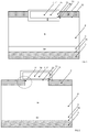
- FIG 11 shows a prior art silicon carbide vertical MOSFET, which comprises a MOS cell between a source side 20 and a drain side 30 with an n doped drain layer 5, an n-doped drift layer 4, a p doped channel layer 42 and two n+ doped source layers 44.
- a MOS cell between a source side 20 and a drain side 30 with an n doped drain layer 5, an n-doped drift layer 4, a p doped channel layer 42 and two n+ doped source layers 44.
- two planar gate electrodes 7' are arranged, each of which comprises a gate layer 70 and an insulating layer 72, which insulates the gate layer 70 from the layers 4, 42, 44 of the MOS cell shown in FIG 11 , wherein an area between the two gate electrodes 7' defines a source opening.
- a source electrode 2 which electrically forms an ohmic contact to the channel layer 42 and the source layers 44.
- JFET junction-FET
- MOSFETs have been introduced, which have a trench planar structure, i.e. a trench gate electrode etched into the wafer with a planar gate layer extending to the lateral sides of the trench gate layer.
- Such prior art devices have lower ON-resistances because of the lack of a JFET region.
- such devices require a highly doped n+ source layer, as well as a p+ contact to the drain electrode to ground the p channel and enable the reverse body diode conduction.
- those doped regions, i.e. source layers and drain layer are formed by implantation and activation, which are limited in dimensions due to lithography accuracy and require a huge thermal budget at about > 1600 °C for > 30 min.
- the source electrode is formed as a Schottky electrode. It acts as a Schottky barrier tunneling source layer, which is connected via a channel of the first conductivity type to the drift layer and a drain sided layer.
- the source layer is formed as a Schottky barrier layer, which is reversely biased during operation, to the drift layer.
- the Schottky barrier layer protects the device from electron injection at zero gate bias.
- Carrier injection in the inventive Schottky barrier MOSFET occurs at high fields at the edge between the gate electrode, Schottky layer and drift layer.
- the electrostatic field of the gate electrode induces an electron tunneling from the source electrode (Schottky metal) through a thin potential barrier. The tunneling current depends on the thickness of the insulating layer of the gate electrode at the edge and the applied gate voltage.
- a Schottky barrier height of 0.9 eV
- oxide thickness 20 nm.
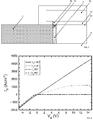
- the drift layer below the gate electrode and along the edge between source electrode and drift layer i.e. downwards in direction of the drain electrode (shown in FIG 3 by the dotted-dashed region) a small amount of tunneling is observed, since the barrier is reversely biased with the drain voltage.
- the high fields in a region of less than 1 nm below the gate electrode generate significantly larger tunneling rates of about a factor of 1 x 10 9 cm 3 higher than compared to regions with a distance of more than 1 nm from the gate electrode.
- carrier injection mainly occurs directly below the gate electrode, other injection can be neglected in the inventive configuration.
- FIG 3 some equipotential tunneling generation densities in the tunneling region are shown, the line closest to the source side 20 having the highest current density and the outermost line having a low current density.
- FIG 4 shows the output (I drain -V drain ) characteristics of an inventive 1.7 kV trench Schottky barrier MOSFET with a drift layer thickness of 15 ⁇ m, a doping level of 4 x 10 15 cm -3 and a Schottky barrier height of 0.9 eV.
- I drain - V drain characteristic is observed for ranging V Gate from - 5 V to + 15 V.
- a slightly larger resistance is observed for V Gate > 0 V, i.e. a sloped characteristics, due to the localized tunneling carrier injection.
- the overall conduction current density in forward direction is very large. In forward direction the resistance is reduced in the inventive device as described above by only 18 %, compared to a prior art reverse diode. Compared to the simulation of conventional MOSFETS in FIG 11 , the forward voltage loss is significantly reduced.
- the inventive Schottky barrier MOSFET shows an "S-shape" in the output, typical for tunneling devices.
- the inventive semiconductor devices achieve for reverse leakage and blocking capability no degradation compared to prior art Schottky barrier diodes.
- the Schottky contact works as the antiparallel freewheeling diode.
- Prior art hybrid devices have been fabricated with separated MOSFET and Schottky diode cells in the active area, with the disadvantage that conduction is lost and thereby high on-state losses are created.
- unipolar devices such as MOSFETs this is a critical feature.
- both MOSFET and diode are included in the same cell, thereby increasing significantly the cell density.
- the on-state current density is higher than for prior art devices due to the absence of channel inversion.
- the built-in internal anti-parallel freewheeling Schottky diode has an opening voltage which is lower than its bipolar body diode counterpart in the prior art MOSFETs.
- the chip area can be used optimally with the inventive design, with MOSFET and diode in the same cell. Therefore, space between the cells can be miniaturized which leads to better input capacitance and consequently also to an improvement for the switching speed of the device.
- the high cell density and therefore high channel density allows for a better current spreading.
- the conduction starts in the channel in the edge below the gate electrode as described above. Once the carriers are injected into the channel, the current spreads within the entire area between two neighboured gate electrodes.
- the inverse doping of the p channel layer (well layer) and drift layer avoids such a current sharing.
- the current sharing capability of the inventive design enables a large forward conduction. Additionally, in the inventive device, short channel effects are suppressed due to enhanced gate electrostatic control at the tunneling junction.
- inventive devices In prior art devices, high activation annealing temperature is needed for activating the n source layer and the p channel layer. However, the high thermal budget degenerates the Si or wide bandgap crystal such as SiC crystal and thus reduces the inversion channel mobility.
- the inventive design does not require an activation anneal, which results in higher carrier mobility than for prior art devices.
- the manufacturing of inventive devices without the need to perform implantation processes reduces costs and improves the semiconductor material interface to the gate electrodes (e.g. Si/wide bandgap material such as SiC as semiconductor material) and an oxide layer as insulating layer of the gate electrode.
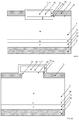
- FIG 1 shows an inventive vertical power semiconductor device comprising from a source side 20 to a drain side 30 opposite to the source side 20 an active cell 6.
- a vertical device is a semiconductor device, in which the source and drain electrode are arranged on opposite sides of the device.
- the device in FIG 1 is a metal oxide semiconductor field-effect transistor (MOSFET).
- MOSFET metal oxide semiconductor field-effect transistor
- Each MOS cell 6 comprises a source electrode 2, a lowly doped drift layer 4 of a first conductivity type, which is in the example shown in FIG 1 an n- doped layer, a drain sided layer in form of a drain layer 5 of the first conductivity type, which is higher doped than the drift layer 4, and a drain electrode 3, which contacts the drain layer 5.
- the cell 6, 6' can either be formed from source electrode 2 to another source electrode (as shown in _ FIG 1 ) or from gate electrode 7 to gate electrode, i.e. shifted from the cell shown in FIG 1 by a half cell.
- the cell is formed by two half cells, wherein each half cell comprises one source electrode 2 and one gate electrode 7. If a plurality of cells are arranged in a device, the cell is formed from the center of a gate electrode to another center of a gate electrode (or center form a source electrode to another center of a gate electrode).
- the doped layers of the device i.e. the drift layer 4 and the drain layer 5, are wide bandgap layers.
- wide bandgap layers are made of silicon carbide.
- the doped layers are silicon layers.
- Wide band gap materials shall be materials having a bandgap of at least 2 eV like silicon carbide, gallium nitride or diamond or such a group-III-Nitride (AlGaln) not excluding other wide bandgap materials.
- the wide bandgap material is SiC (silicon carbide), exemplarily 3 C, 4 H or 6 H SiC.
- the doping concentration and thickness of the drift layer 4 are chosen.
- the drift layer 4 has a doping concentration between 1 x 10 12 and 5 x 10 17 cm -3 and a thickness between 3 ⁇ m to 250 ⁇ m. The thicknesses shall be measured in depth direction, i.e. in a direction vertical to the source side 20.
- the drift layer 4 has a constantly low doping concentration.
- the substantially constant doping concentration of the drift layer 4 shall mean that the doping concentration is substantially homogeneous throughout the drift layer 4, however without excluding that fluctuations in the doping concentration within the drift layer being in the order of a factor of one to five.
- the source electrode 2 On the source side 20 of the SiC wafer a source electrode 2 is arranged which forms a Schottky contact to the drift layer 4.
- the source electrode 2 may have a Schottky barrier height between 0.5 eV to 2 eV or between 0.7 eV to 1.1 eV.
- the source electrode 2 is a metal layer, such as titanium (Ti), cobalt (Co), tantalum (Ta), tungsten (W), platinum (Pt), nickel (Ni), molybdenum (Mo), palladium (Pd), aluminium or any combination of these metals.
- the source electrode 2 can also include silicide or carbide compounds, such as Ni X Si Y , TiC, TaC or WC.
- the source electrode 2 can also be a stack of metal layers, e.g. Al/Ti, Al/Ni, Al/W, Al/Pt, Al/Ni/Ti, Al/Mo, Al/Pd, Al/WC, or Al/TaC, in which a diffusion barrier layer like TaSiN can be formed in between the top Al and the first metal layer.
- metal layers e.g. Al/Ti, Al/Ni, Al/W, Al/Pt, Al/Ni/Ti, Al/Mo, Al/Pd, Al/WC, or Al/TaC, in which a diffusion barrier layer like TaSiN can be formed in between the top Al and the first metal layer.
- An ohmic contact is an electrical junction between two conductors (i.e. for a semiconductor between a metal layer and a semiconductor layer, i.e. a doped Silicon-carbide layer) that has a linear current-voltage behavior.
- An ohmic contact has low resistance.
- the ohmic contacts on the drain side form a drain electrode for an inventive MOSFET.
- a Schottky contact is a junction or contact that does not demonstrate a linear I-V curve (so that it is a non-ohmic contact).
- the Schottky barrier of a Schottky contact between a metal and a semiconductor band defines the device opening voltage in forward bias, i.e., carrier flows when the barrier is overcome.
- n doped drain layer 5 is arranged on the drain side 30, which has a higher doping concentration than the drift layer 4.
- the doping concentration of the drain layer 5 is above 1 x 10 18 , exemplarily between 5 x 10 18 and 1 x 10 20 cm -3 .
- the drain layer 5 attaches towards the source side 20 the drift layer 4 and contacts on the drain side 30 a drain electrode 3 formed as an ohmic contact.
- the doping concentration of the drain layer 5 is at least a factor of 1000 higher than the doping concentration of the drift layer 4.
- a gate electrode 7, 7', 7" is arranged on the source side 20 and comprises an electrically conductive gate layer 70 and an insulating layer 72, which insulates the gate layer 70 from the source electrode 2 and the drift layer 4 (and any other doped layer).
- the inversion-channel is called a MOS channel (metal-oxide/insulator-semiconductor), whereas otherwise (insulating layer 72 being made of any insulating materials; e.g. dielectrics such as high-k materials or silicate glasses such as PSG (phosphorous silicate glass, also called phosphosilicate glass) or BPSG (boron phosphorous silicate glass, also called borophosphosilicate glass), but not excluding other insulators) the channel may also be called MIS channel (metal-insulator-semiconductor).
- MOS channel metal-oxide/insulator-semiconductor
- any appropriate electrically conductive material like a metal or doped polycrystalline silicon may be used.
- the term MOS device/MOSFET shall also cover such MIS devices/ MISFETs.
- the inventive MOSFETs shall exemplarily have a rated voltage of at least 100 V or at least 200 V.
- the gate electrode 7 may be a planar gate electrode 7', which is arranged on top of the SiC wafer (shown in FIG 2 ).
- the insulating layer 72 is arranged on top of the drift layer 4 with an insulating layer thickness between the gate layer 70 and the drift layer 4.
- the insulating layer 72 has a thickness 76 at an edge 74 of insulating layer with the source electrode 2 and the drift layer 4. Exemplarily, this thickness is constant between the gate layer 70 and the drift layer 4.
- the gate layer 70 is separated from the drift layer 4 by the insulating layer 72.
- the gate layer is embedded in the insulating layer 72, i.e. the insulating layer 72 surrounds the gate layer towards the lower side (i.e. towards the drift layer 4), the lateral sides (i.e. the sides perpendicular to the source side 20) and the top side.
- the insulating layer may have a greater thickness on those side than towards the drift layer 4.
- the gate layer 70 has an overlap with the below lying source electrode 2 in vertical direction to the source side 20 (which shall be the outermost plane of the SiC wafer on the side, at which the source electrode 2 is arranged).
- the gate electrode 7, 7', 7" i.e. the insulating layer 72, the source electrode 2 and the drift layer 4 attach each other at an edge 74.
- a thickness 76 of the insulating layer 72 at the edge 74 is chosen such that a maximum electric field at the maximum rated voltage is below 5 MeV/cm in the device. In an exemplary embodiment, the maximum electric field is below 2 MeV/cm.
- the thickness 76 of the insulating layer 72 at the edge 76 may exemplarily be between 1 to 100 nm or between 10 nm to 100 nm.
- the thickness 76 of the insulating layer shall be measured as the shortest extension of the insulating layer 72 between the gate layer 70 and the drift layer 4 at the edge 74.
- Such a thickness enables the device to have a tunnelling effect of charges at the edge region (as shown in FIG 3 by the high current densities in the drift layer at the edge, i.e. just below the gate electrode 7. Due to the tunneling at the edge 74 a MOS channel may be formed from the source electrode 2 to the drift layer 4 in such a cell 6.
- the inventive device may comprise a trench gate electrode 7" ( FIG 1 ), for which a trench has been introduced perpendicular to the source side 20 laterally to the source electrode 2.
- the trench gate electrode 7" is arranged in the same plane as the source electrode 2, i.e. the trench gate electrode 7" and source electrode 2 alternate and attach each other.
- the insulating layer 74 covers the walls of the trenches towards the wide band gap layers and separates the gate layer 70, with which the trenches are filled, from the wide bandgap layers.
- the insulating layer 72 separates the gate layer 70 from the source electrode 2.
- the gate layer 70 extends to a greater depth than the source electrode 2 in vertical direction to the source side 20.
- the insulating layer 72 has a thickness 76 at the edge of the insulating layer 72 with the drift layer 4 and the source electrode 2.
- the insulating layer 72 may have a larger thickness 78 below the gate layer 70 to achieve a better insulation effect.
- the power semiconductor device may comprise just one MOS cell as shown in FIG 1 or 2 , but in an exemplary embodiment, an inventive MOSFET comprises a plurality of cells 6, 6', i.e. two or more cells 6, 6'.
- the cells 6, 6' may be formed by lateral repetition of the cell 6 as exemplarily shown in FIG 1 or 2 .
- Such cells 6 may be arranged receptively to the lateral sides of the MOS cell 6, i.e. the source electrode 2 may be continued to form also a source electrode 2 of a neighboured MOS cell 6.
- the right source electrode of the left handed cell 6 forms a continuous source electrode 2 with the left source electrode 2 of the right handed cell 6', so that the two source electrodes 2 of neighboured cells facing each other form a common source electrode 2.
- the cells 6, 6', i.e. the regions in the cells may be designed to form of regular patterns like stripes, hexagonal, triangular or square design. Such MOS cells may be interconnected to each other.
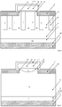
- FIG 5 shows exemplarily an inventive MOSFET with two cells 6, 6'.
- two neighboured cells 6, 6' may have a cell pitch 60 (width of the cell) of at least 20 nm or of at most 20 ⁇ m or between 20 nm to 20 ⁇ m.
- the device comprises in a direction perpendicular to the source side 20 the drift layer 4 comprising a plurality of regions 40 of the first conductivity type (i.e. n- doped in case of the drift layer being of the n doping type) and a plurality of regions 8 of the second conductivity type (i.e. p doping type in the present example).
- the n- and p doped regions 40, 8 alternate in a plane parallel to the source side 20.
- these regions extend from the source side 20 (below the gate electrode 7, 7', 7" and the source electrode 2) to the drain sided layer 5 (or the collector layer 55 in case of a NPT-IGBT or the buffer layer 46 in case of a PT-IGBT), i.e. they are in touch with the drain layer 5, by which arrangement a super-junction device is formed.
- the n doped regions 40 are arranged at the edges 74 of the gate electrode 7, 7', 7" and the p doped regions 8 are arranged at lateral sides (i.e. lateral in a plane parallel to the source side 20) and therefore, to the n doped regions 40 at the edge 74.
- the p doped regions 8 extend to an area within the drift layer 4, so that the drift layer 4 separates the p doped regions 8 from the drain layer 5 ( FIG 7 ).
- the drift layer 4 separates the p doped regions 8 from the drain sided layer, the collector layer in case of a NPT-IGBT or the buffer layer 46 in case of a PT-IGBT.
- the p doped regions 8 extend to the source electrode 2 and the gate electrode 7.
- a p doped protection layer 9 may be arranged below the gate electrode 7, 7', 7" and in contact to it, i.e. in contact to the insulating layer 72.
- the maximum doping concentration of the protection layer may be at least 1 x 10 18 cm -3 .
- An inventive MOSFET may be operated by applying a positive voltage at the gate layer such that enabling a tunnelling of electrons from the source electrode to the drift layer in an area directly below the gate electrode.
- a positive voltage at the gate layer By applying the positive voltage at the gate layer a maximum electric field at the maximum rated voltage is kept below 5 MeV/cm in the device.
- the voltage at the gate layer is at least + 10 V.
- a drain sided layer 5, 55 is arranged, which is in the case of the inventive device being a MOSFET an n doped drain layer 5.
- the inventive cell 6, 6' is integrated into an inventive insulated gate bipolar transistor (IGBT), for which on the drain side 30 a p doped collector layer 55 is arranged as drain sided layer instead of the n doped drain layer for the MOSFET.
- FIG 9 shows exemplarily a non-punch through IGBT with trench gate electrode 7" and FIG 10 a non-punch through IGBT with planar gate electrode 7'.
- the inventive cell 6, 6' can be applied to a non punch-through IGBT, which comprises on the drain side 30 a p doped collector layer 55, which has exemplarily has exemplarily a doping concentration between 1 * 10 18 and 1 * 10 20 cm -3 .
- the collector layer 55 contacts the drain electrode 3 (which may also be called collector electrode in an IGBT) as an ohmic contact.
- the collector layer 55 contacts towards the source side 20 the drift layer 4.
- the source electrode 2 may also be called emitter electrode for an IGBT.
- the inventive cell 6, 6' may also be applied to a punch-through IGBT (i.e. an IGBT with a buffer layer 46, which additionally comprises between the drift layer 4 and the collector layer 55 an n doped buffer layer 46, which has a higher doping concentration than the drift layer 4).
- a punch-through IGBT i.e. an IGBT with a buffer layer 46, which additionally comprises between the drift layer 4 and the collector layer 55 an n doped buffer layer 46, which has a higher doping concentration than the drift layer 4.
- the buffer layer 46 is drawn by a dashed line, thereby indicating that this layer is an optional layer, which is present in a punch-through IGBT, but omitted in a non punch-through IGBT.
- the buffer layer 46 may have an exemplary doping concentration between 1 * 10 17 and 1 * 10 18 cm -3 and a thickness up to 3 ⁇ m.
- the E-field is triangular in shape up to avalanche breakdown. In the other case the E-field penetrates through the interface between drift layer 4 and buffer layer 46 where it gets stopped due to the high doping concentration of the buffer layer 46.
- the inventive cell 6, 6' may be applied to a reverse-conducting IGBT, which comprises additionally to the non punch-through IGBT or punch-through IGBT an n doped cathode layer, which comprises a plurality of cathode regions.
- the collector layer 55 also comprises a plurality of collector regions 55.
- the cathode layer is higher doped than the drift layer 4, and, if a buffer layer 46 is arranged between drift and collector layer 4, 55, the cathode layer has also higher doping concentration than the buffer layer 46.
- Cathode and collector regions are arranged alternatingly on the drain side 30 and contact the collector electrode 3.
- an inventive reverse-conducting IGBT is formed as a Bi-mode Insulated Gate Transistor (BIGT) additionally having a large pilot p+ collector layer in the central part of the device on the drain side 30 surrounded by alternating smaller p+ collector regions and n+ cathode regions.
- BIGT Bi-mode Insulated Gate Transistor
- the values for the doping concentration given above shall be understood as the mean doping concentration for the exemplarily constant doping concentration of the layers (not excluding variation of doping concentration due to imperfection of the manufacturing method).
- the conductivity types of the layers are switched, i.e. all layers of the first conductivity type are p type (e.g. the drift layer 4 and the drain layer 5) and all layers of the second conductivity type are n type (e.g. region of the second conductivity type and the protection layer 9).
Landscapes
- Electrodes Of Semiconductors (AREA)
Priority Applications (1)
| Application Number | Priority Date | Filing Date | Title |
|---|---|---|---|
| EP16173688.9A EP3255676A1 (fr) | 2016-06-09 | 2016-06-09 | Dispositif à semi-conducteur de puissance verticale et procédé pour faire fonctionner un tel dispositif |
Applications Claiming Priority (1)
| Application Number | Priority Date | Filing Date | Title |
|---|---|---|---|
| EP16173688.9A EP3255676A1 (fr) | 2016-06-09 | 2016-06-09 | Dispositif à semi-conducteur de puissance verticale et procédé pour faire fonctionner un tel dispositif |
Publications (1)
| Publication Number | Publication Date |
|---|---|
| EP3255676A1 true EP3255676A1 (fr) | 2017-12-13 |
Family
ID=56116368
Family Applications (1)
| Application Number | Title | Priority Date | Filing Date |
|---|---|---|---|
| EP16173688.9A Withdrawn EP3255676A1 (fr) | 2016-06-09 | 2016-06-09 | Dispositif à semi-conducteur de puissance verticale et procédé pour faire fonctionner un tel dispositif |
Country Status (1)
| Country | Link |
|---|---|
| EP (1) | EP3255676A1 (fr) |
Cited By (8)
| Publication number | Priority date | Publication date | Assignee | Title |
|---|---|---|---|---|
| CN112599603A (zh) * | 2020-12-16 | 2021-04-02 | 西安电子科技大学 | 基于纵向肖特基源隧穿结的准垂直场效应晶体管及方法 |
| CN112614884A (zh) * | 2020-12-16 | 2021-04-06 | 西安电子科技大学 | 基于纵向肖特基隧穿发射结的半导体垂直igbt及制备方法 |
| CN112614888A (zh) * | 2020-12-16 | 2021-04-06 | 西安电子科技大学 | 基于横向肖特基源隧穿结的准垂直场效应晶体管及方法 |
| CN112614890A (zh) * | 2020-12-16 | 2021-04-06 | 西安电子科技大学 | 基于横向肖特基源隧穿结的全垂直场效应晶体管及方法 |
| CN112614883A (zh) * | 2020-12-16 | 2021-04-06 | 西安电子科技大学 | 基于横向肖特基隧穿发射结的半导体垂直igbt及制备方法 |
| CN112614889A (zh) * | 2020-12-16 | 2021-04-06 | 西安电子科技大学 | 基于纵向肖特基源隧穿结的全垂直场效应晶体管及方法 |
| CN114207836A (zh) * | 2019-08-01 | 2022-03-18 | 日立能源瑞士股份公司 | 碳化硅晶体管器件 |
| EP4009375B1 (fr) * | 2020-12-03 | 2024-03-06 | Hitachi Energy Ltd | Dispositif à semi-conducteurs de puissance et procédé pour la fabrication de dispositif à semi-conducteurs de puissance |
Citations (5)
| Publication number | Priority date | Publication date | Assignee | Title |
|---|---|---|---|---|
| EP0348916A2 (fr) * | 1988-06-27 | 1990-01-03 | Nissan Motor Co., Ltd. | Dispositif à semiconducteur équivalent à un MOSFET pour la commande de tension |
| DE10227831A1 (de) * | 2002-06-21 | 2004-01-15 | Infineon Technologies Ag | Schaltwandler |
| US8212283B2 (en) | 2009-04-29 | 2012-07-03 | Abb Technology Ag | Reverse-conducting semiconductor device |
| FR2975531A1 (fr) * | 2011-05-16 | 2012-11-23 | St Microelectronics Tours Sas | Diode schottky verticale controlee |
| US20140167205A1 (en) * | 2012-12-13 | 2014-06-19 | Pfc Device Holdings Limited | Super junction for semiconductor device and method for manufacturing the same |
-
2016
- 2016-06-09 EP EP16173688.9A patent/EP3255676A1/fr not_active Withdrawn
Patent Citations (5)
| Publication number | Priority date | Publication date | Assignee | Title |
|---|---|---|---|---|
| EP0348916A2 (fr) * | 1988-06-27 | 1990-01-03 | Nissan Motor Co., Ltd. | Dispositif à semiconducteur équivalent à un MOSFET pour la commande de tension |
| DE10227831A1 (de) * | 2002-06-21 | 2004-01-15 | Infineon Technologies Ag | Schaltwandler |
| US8212283B2 (en) | 2009-04-29 | 2012-07-03 | Abb Technology Ag | Reverse-conducting semiconductor device |
| FR2975531A1 (fr) * | 2011-05-16 | 2012-11-23 | St Microelectronics Tours Sas | Diode schottky verticale controlee |
| US20140167205A1 (en) * | 2012-12-13 | 2014-06-19 | Pfc Device Holdings Limited | Super junction for semiconductor device and method for manufacturing the same |
Cited By (11)
| Publication number | Priority date | Publication date | Assignee | Title |
|---|---|---|---|---|
| CN114207836A (zh) * | 2019-08-01 | 2022-03-18 | 日立能源瑞士股份公司 | 碳化硅晶体管器件 |
| US12062698B2 (en) | 2019-08-01 | 2024-08-13 | Hitachi Energy Ltd | Silicon carbide transistor device |
| EP4009375B1 (fr) * | 2020-12-03 | 2024-03-06 | Hitachi Energy Ltd | Dispositif à semi-conducteurs de puissance et procédé pour la fabrication de dispositif à semi-conducteurs de puissance |
| US20240096937A1 (en) * | 2020-12-03 | 2024-03-21 | Hitachi Energy Switzerland Ag | Power semiconductor device and a method for producing a power semiconductor device |
| US12501668B2 (en) * | 2020-12-03 | 2025-12-16 | Hitachi Energy Ltd | Power semiconductor device and a method for producing a power semiconductor device |
| CN112599603A (zh) * | 2020-12-16 | 2021-04-02 | 西安电子科技大学 | 基于纵向肖特基源隧穿结的准垂直场效应晶体管及方法 |
| CN112614884A (zh) * | 2020-12-16 | 2021-04-06 | 西安电子科技大学 | 基于纵向肖特基隧穿发射结的半导体垂直igbt及制备方法 |
| CN112614888A (zh) * | 2020-12-16 | 2021-04-06 | 西安电子科技大学 | 基于横向肖特基源隧穿结的准垂直场效应晶体管及方法 |
| CN112614890A (zh) * | 2020-12-16 | 2021-04-06 | 西安电子科技大学 | 基于横向肖特基源隧穿结的全垂直场效应晶体管及方法 |
| CN112614883A (zh) * | 2020-12-16 | 2021-04-06 | 西安电子科技大学 | 基于横向肖特基隧穿发射结的半导体垂直igbt及制备方法 |
| CN112614889A (zh) * | 2020-12-16 | 2021-04-06 | 西安电子科技大学 | 基于纵向肖特基源隧穿结的全垂直场效应晶体管及方法 |
Similar Documents
| Publication | Publication Date | Title |
|---|---|---|
| EP3255676A1 (fr) | Dispositif à semi-conducteur de puissance verticale et procédé pour faire fonctionner un tel dispositif | |
| EP2264769B1 (fr) | Dispositif à semi-conducteur à grille tamponnée à canal horizontal au carbure de silicium | |
| US9159796B2 (en) | Method for protecting a semiconductor device against degradation and a method for manufacturing a semiconductor device protected against hot charge carriers | |
| US9570607B2 (en) | Field-effect semiconductor device having alternating n-type and p-type pillar regions arranged in an active area | |
| US20170170264A1 (en) | Semiconductor Devices and a Circuit for Controlling a Field Effect Transistor of a Semiconductor Device | |
| CN103915485B (zh) | 电荷补偿半导体器件 | |
| US9502402B2 (en) | Semiconductor device | |
| JPWO2019077877A1 (ja) | 炭化珪素半導体装置および炭化珪素半導体装置の製造方法 | |
| US10297685B2 (en) | Semiconductor device | |
| US20120187526A1 (en) | Method of forming a semiconductor device termination and structure therefor | |
| EP3327791A1 (fr) | Transistor à effet de champ à jonction | |
| JP2021028962A (ja) | 炭化珪素半導体装置 | |
| WO2022199955A1 (fr) | Dispositif à semi-conducteur de puissance et son procédé de production | |
| EP4009379B1 (fr) | Dispositif de puissance à électrode de grille en tranché isolée | |
| CN114864677A (zh) | 晶体管器件及其制造方法 | |
| JP2019083354A (ja) | 半導体装置 | |
| EP3182463A1 (fr) | Dispositif à semi-conducteur de puissance à blocage inverse | |
| JP2014508406A (ja) | オン抵抗が低減された半導体装置 | |
| US20230163167A1 (en) | Semiconductor device including a trench gate structure | |
| KR102719789B1 (ko) | 낮은 작동 전압을 갖는 npnp 층상 mos 게이트 트렌치 디바이스 | |
| EP3223316A1 (fr) | Dispositif semi-conducteur à large structure de bande et son procédé de fabrication | |
| US20240055505A1 (en) | Semiconductor device | |
| HK40093245A (zh) | 具有降低的操作电压的npnp分层mos栅控沟槽装置 | |
| US9502498B2 (en) | Power semiconductor device |
Legal Events
| Date | Code | Title | Description |
|---|---|---|---|
| PUAI | Public reference made under article 153(3) epc to a published international application that has entered the european phase |
Free format text: ORIGINAL CODE: 0009012 |
|
| STAA | Information on the status of an ep patent application or granted ep patent |
Free format text: STATUS: THE APPLICATION HAS BEEN PUBLISHED |
|
| AK | Designated contracting states |
Kind code of ref document: A1 Designated state(s): AL AT BE BG CH CY CZ DE DK EE ES FI FR GB GR HR HU IE IS IT LI LT LU LV MC MK MT NL NO PL PT RO RS SE SI SK SM TR |
|
| AX | Request for extension of the european patent |
Extension state: BA ME |
|
| STAA | Information on the status of an ep patent application or granted ep patent |
Free format text: STATUS: THE APPLICATION HAS BEEN WITHDRAWN |
|
| 18W | Application withdrawn |
Effective date: 20180214 |