EP3255693B1 - Élément électroluminescent organique et dispositif électronique - Google Patents
Élément électroluminescent organique et dispositif électronique Download PDFInfo
- Publication number
- EP3255693B1 EP3255693B1 EP16746638.2A EP16746638A EP3255693B1 EP 3255693 B1 EP3255693 B1 EP 3255693B1 EP 16746638 A EP16746638 A EP 16746638A EP 3255693 B1 EP3255693 B1 EP 3255693B1
- Authority
- EP
- European Patent Office
- Prior art keywords
- group
- compound
- carbon atoms
- substituted
- ring
- Prior art date
- Legal status (The legal status is an assumption and is not a legal conclusion. Google has not performed a legal analysis and makes no representation as to the accuracy of the status listed.)
- Active
Links
Images

Classifications
-
- C—CHEMISTRY; METALLURGY
- C09—DYES; PAINTS; POLISHES; NATURAL RESINS; ADHESIVES; COMPOSITIONS NOT OTHERWISE PROVIDED FOR; APPLICATIONS OF MATERIALS NOT OTHERWISE PROVIDED FOR
- C09K—MATERIALS FOR MISCELLANEOUS APPLICATIONS, NOT PROVIDED FOR ELSEWHERE
- C09K11/00—Luminescent materials, e.g. electroluminescent or chemiluminescent
- C09K11/06—Luminescent materials, e.g. electroluminescent or chemiluminescent containing organic luminescent materials
-
- C—CHEMISTRY; METALLURGY
- C09—DYES; PAINTS; POLISHES; NATURAL RESINS; ADHESIVES; COMPOSITIONS NOT OTHERWISE PROVIDED FOR; APPLICATIONS OF MATERIALS NOT OTHERWISE PROVIDED FOR
- C09K—MATERIALS FOR MISCELLANEOUS APPLICATIONS, NOT PROVIDED FOR ELSEWHERE
- C09K11/00—Luminescent materials, e.g. electroluminescent or chemiluminescent
- C09K11/02—Use of particular materials as binders, particle coatings or suspension media therefor
- C09K11/025—Use of particular materials as binders, particle coatings or suspension media therefor non-luminescent particle coatings or suspension media
-
- H—ELECTRICITY
- H10—SEMICONDUCTOR DEVICES; ELECTRIC SOLID-STATE DEVICES NOT OTHERWISE PROVIDED FOR
- H10K—ORGANIC ELECTRIC SOLID-STATE DEVICES
- H10K50/00—Organic light-emitting devices
- H10K50/10—OLEDs or polymer light-emitting diodes [PLED]
- H10K50/11—OLEDs or polymer light-emitting diodes [PLED] characterised by the electroluminescent [EL] layers
-
- H—ELECTRICITY
- H10—SEMICONDUCTOR DEVICES; ELECTRIC SOLID-STATE DEVICES NOT OTHERWISE PROVIDED FOR
- H10K—ORGANIC ELECTRIC SOLID-STATE DEVICES
- H10K50/00—Organic light-emitting devices
- H10K50/10—OLEDs or polymer light-emitting diodes [PLED]
- H10K50/11—OLEDs or polymer light-emitting diodes [PLED] characterised by the electroluminescent [EL] layers
- H10K50/12—OLEDs or polymer light-emitting diodes [PLED] characterised by the electroluminescent [EL] layers comprising dopants
- H10K50/121—OLEDs or polymer light-emitting diodes [PLED] characterised by the electroluminescent [EL] layers comprising dopants for assisting energy transfer, e.g. sensitization
-
- H—ELECTRICITY
- H10—SEMICONDUCTOR DEVICES; ELECTRIC SOLID-STATE DEVICES NOT OTHERWISE PROVIDED FOR
- H10K—ORGANIC ELECTRIC SOLID-STATE DEVICES
- H10K85/00—Organic materials used in the body or electrodes of devices covered by this subclass
- H10K85/30—Coordination compounds
- H10K85/321—Metal complexes comprising a group IIIA element, e.g. Tris (8-hydroxyquinoline) gallium [Gaq3]
- H10K85/322—Metal complexes comprising a group IIIA element, e.g. Tris (8-hydroxyquinoline) gallium [Gaq3] comprising boron
-
- H—ELECTRICITY
- H10—SEMICONDUCTOR DEVICES; ELECTRIC SOLID-STATE DEVICES NOT OTHERWISE PROVIDED FOR
- H10K—ORGANIC ELECTRIC SOLID-STATE DEVICES
- H10K85/00—Organic materials used in the body or electrodes of devices covered by this subclass
- H10K85/60—Organic compounds having low molecular weight
- H10K85/615—Polycyclic condensed aromatic hydrocarbons, e.g. anthracene
-
- H—ELECTRICITY
- H10—SEMICONDUCTOR DEVICES; ELECTRIC SOLID-STATE DEVICES NOT OTHERWISE PROVIDED FOR
- H10K—ORGANIC ELECTRIC SOLID-STATE DEVICES
- H10K85/00—Organic materials used in the body or electrodes of devices covered by this subclass
- H10K85/60—Organic compounds having low molecular weight
- H10K85/631—Amine compounds having at least two aryl rest on at least one amine-nitrogen atom, e.g. triphenylamine
- H10K85/633—Amine compounds having at least two aryl rest on at least one amine-nitrogen atom, e.g. triphenylamine comprising polycyclic condensed aromatic hydrocarbons as substituents on the nitrogen atom
-
- H—ELECTRICITY
- H10—SEMICONDUCTOR DEVICES; ELECTRIC SOLID-STATE DEVICES NOT OTHERWISE PROVIDED FOR
- H10K—ORGANIC ELECTRIC SOLID-STATE DEVICES
- H10K85/00—Organic materials used in the body or electrodes of devices covered by this subclass
- H10K85/60—Organic compounds having low molecular weight
- H10K85/649—Aromatic compounds comprising a hetero atom
- H10K85/654—Aromatic compounds comprising a hetero atom comprising only nitrogen as heteroatom
-
- H—ELECTRICITY
- H10—SEMICONDUCTOR DEVICES; ELECTRIC SOLID-STATE DEVICES NOT OTHERWISE PROVIDED FOR
- H10K—ORGANIC ELECTRIC SOLID-STATE DEVICES
- H10K85/00—Organic materials used in the body or electrodes of devices covered by this subclass
- H10K85/60—Organic compounds having low molecular weight
- H10K85/649—Aromatic compounds comprising a hetero atom
- H10K85/657—Polycyclic condensed heteroaromatic hydrocarbons
-
- H—ELECTRICITY
- H10—SEMICONDUCTOR DEVICES; ELECTRIC SOLID-STATE DEVICES NOT OTHERWISE PROVIDED FOR
- H10K—ORGANIC ELECTRIC SOLID-STATE DEVICES
- H10K85/00—Organic materials used in the body or electrodes of devices covered by this subclass
- H10K85/60—Organic compounds having low molecular weight
- H10K85/649—Aromatic compounds comprising a hetero atom
- H10K85/657—Polycyclic condensed heteroaromatic hydrocarbons
- H10K85/6572—Polycyclic condensed heteroaromatic hydrocarbons comprising only nitrogen in the heteroaromatic polycondensed ring system, e.g. phenanthroline or carbazole
-
- H—ELECTRICITY
- H10—SEMICONDUCTOR DEVICES; ELECTRIC SOLID-STATE DEVICES NOT OTHERWISE PROVIDED FOR
- H10K—ORGANIC ELECTRIC SOLID-STATE DEVICES
- H10K85/00—Organic materials used in the body or electrodes of devices covered by this subclass
- H10K85/60—Organic compounds having low molecular weight
- H10K85/649—Aromatic compounds comprising a hetero atom
- H10K85/657—Polycyclic condensed heteroaromatic hydrocarbons
- H10K85/6574—Polycyclic condensed heteroaromatic hydrocarbons comprising only oxygen in the heteroaromatic polycondensed ring system, e.g. cumarine dyes
-
- C—CHEMISTRY; METALLURGY
- C09—DYES; PAINTS; POLISHES; NATURAL RESINS; ADHESIVES; COMPOSITIONS NOT OTHERWISE PROVIDED FOR; APPLICATIONS OF MATERIALS NOT OTHERWISE PROVIDED FOR
- C09K—MATERIALS FOR MISCELLANEOUS APPLICATIONS, NOT PROVIDED FOR ELSEWHERE
- C09K2211/00—Chemical nature of organic luminescent or tenebrescent compounds
- C09K2211/10—Non-macromolecular compounds
- C09K2211/1003—Carbocyclic compounds
- C09K2211/1007—Non-condensed systems
-
- C—CHEMISTRY; METALLURGY
- C09—DYES; PAINTS; POLISHES; NATURAL RESINS; ADHESIVES; COMPOSITIONS NOT OTHERWISE PROVIDED FOR; APPLICATIONS OF MATERIALS NOT OTHERWISE PROVIDED FOR
- C09K—MATERIALS FOR MISCELLANEOUS APPLICATIONS, NOT PROVIDED FOR ELSEWHERE
- C09K2211/00—Chemical nature of organic luminescent or tenebrescent compounds
- C09K2211/10—Non-macromolecular compounds
- C09K2211/1003—Carbocyclic compounds
- C09K2211/1011—Condensed systems
-
- C—CHEMISTRY; METALLURGY
- C09—DYES; PAINTS; POLISHES; NATURAL RESINS; ADHESIVES; COMPOSITIONS NOT OTHERWISE PROVIDED FOR; APPLICATIONS OF MATERIALS NOT OTHERWISE PROVIDED FOR
- C09K—MATERIALS FOR MISCELLANEOUS APPLICATIONS, NOT PROVIDED FOR ELSEWHERE
- C09K2211/00—Chemical nature of organic luminescent or tenebrescent compounds
- C09K2211/10—Non-macromolecular compounds
- C09K2211/1003—Carbocyclic compounds
- C09K2211/1014—Carbocyclic compounds bridged by heteroatoms, e.g. N, P, Si or B
-
- C—CHEMISTRY; METALLURGY
- C09—DYES; PAINTS; POLISHES; NATURAL RESINS; ADHESIVES; COMPOSITIONS NOT OTHERWISE PROVIDED FOR; APPLICATIONS OF MATERIALS NOT OTHERWISE PROVIDED FOR
- C09K—MATERIALS FOR MISCELLANEOUS APPLICATIONS, NOT PROVIDED FOR ELSEWHERE
- C09K2211/00—Chemical nature of organic luminescent or tenebrescent compounds
- C09K2211/10—Non-macromolecular compounds
- C09K2211/1018—Heterocyclic compounds
-
- H—ELECTRICITY
- H10—SEMICONDUCTOR DEVICES; ELECTRIC SOLID-STATE DEVICES NOT OTHERWISE PROVIDED FOR
- H10K—ORGANIC ELECTRIC SOLID-STATE DEVICES
- H10K2101/00—Properties of the organic materials covered by group H10K85/00
-
- H—ELECTRICITY
- H10—SEMICONDUCTOR DEVICES; ELECTRIC SOLID-STATE DEVICES NOT OTHERWISE PROVIDED FOR
- H10K—ORGANIC ELECTRIC SOLID-STATE DEVICES
- H10K2101/00—Properties of the organic materials covered by group H10K85/00
- H10K2101/20—Delayed fluorescence emission
-
- H—ELECTRICITY
- H10—SEMICONDUCTOR DEVICES; ELECTRIC SOLID-STATE DEVICES NOT OTHERWISE PROVIDED FOR
- H10K—ORGANIC ELECTRIC SOLID-STATE DEVICES
- H10K2101/00—Properties of the organic materials covered by group H10K85/00
- H10K2101/30—Highest occupied molecular orbital [HOMO], lowest unoccupied molecular orbital [LUMO] or Fermi energy values
-
- H—ELECTRICITY
- H10—SEMICONDUCTOR DEVICES; ELECTRIC SOLID-STATE DEVICES NOT OTHERWISE PROVIDED FOR
- H10K—ORGANIC ELECTRIC SOLID-STATE DEVICES
- H10K50/00—Organic light-emitting devices
- H10K50/10—OLEDs or polymer light-emitting diodes [PLED]
- H10K50/14—Carrier transporting layers
- H10K50/15—Hole transporting layers
-
- H—ELECTRICITY
- H10—SEMICONDUCTOR DEVICES; ELECTRIC SOLID-STATE DEVICES NOT OTHERWISE PROVIDED FOR
- H10K—ORGANIC ELECTRIC SOLID-STATE DEVICES
- H10K50/00—Organic light-emitting devices
- H10K50/10—OLEDs or polymer light-emitting diodes [PLED]
- H10K50/14—Carrier transporting layers
- H10K50/16—Electron transporting layers
-
- H—ELECTRICITY
- H10—SEMICONDUCTOR DEVICES; ELECTRIC SOLID-STATE DEVICES NOT OTHERWISE PROVIDED FOR
- H10K—ORGANIC ELECTRIC SOLID-STATE DEVICES
- H10K85/00—Organic materials used in the body or electrodes of devices covered by this subclass
- H10K85/60—Organic compounds having low molecular weight
- H10K85/615—Polycyclic condensed aromatic hydrocarbons, e.g. anthracene
- H10K85/622—Polycyclic condensed aromatic hydrocarbons, e.g. anthracene containing four rings, e.g. pyrene
Definitions
- the present invention relates to an organic electroluminescence device and an electronic device.
- organic electroluminescence device When a voltage is applied to an organic electroluminescence device (hereinafter, occasionally referred to as "organic EL device"), holes and electrons are injected into an emitting layer respectively from an anode and a cathode. The injected holes and electrons are recombined to generate excitons in the emitting layer. According to the electron spin statistics theory, singlet excitons are generated at a ratio of 25% and triplet excitons are generated at a ratio of 75%.
- a fluorescent organic EL device which uses emission caused by singlet excitons, is applied to a full color display of a mobile phone, a TV set and the like. It has been studied to further improve a performance of the fluorescent organic EL device. For instance, in order to further improve a luminous efficiency, an organic EL device with use of singlet excitons and triplet excitons has been studied.
- thermally activated delayed fluorescence refers to, for instance, " ADACHI, Chihaya, ed. (March 22, 2012), "Yuki Hando-tai no Debaisu Bussei (Device Physics of Organic Semiconductors)", Kodansha, pp. 261-262 .”
- non-Patent Literatures 1 and 2 also disclose organic EL devices using the TADF mechanism.
- Non-Patent Literature 1 Hajime Nakanotani, et al (9 persons), "High-Efficiency organic light-emitting diodes with fluorescent emitters", NATURE COMMUNICATIONS, in May 30, 2014, 5, 4016 (DOI: 10.1038/ncomms5016 )
- Non-Patent Literature 2 Dongdong Zhang, et al (6 persons), "High-Efficiency Fluorescent Organic Light-Emitting Devices Using Sensitizing Hosts with a Small Singlet-Triplet Exchange Energy", ADVANCED MATERIALS, 2014 (DOI: 10.1002/adma.201401476 )
- WO 2014/157619 A1 discloses inter alia an OLED device (Example 5) comprising an anode, a hole transporting layer ( ⁇ -NPD), a luminescent layer comprising ZHSO2 as a thermally activated delayed fluorescence (TADF) first compound and 4CzTPN-Ph as a red (> 550 nm) emitting fluorescent second compound, an electron transporting layer (TmPyPb), and a cathode.
- TADF thermally activated delayed fluorescence
- TmPyPb electron transporting layer
- an organic electroluminescence device as defined in any of claims 1 to 12 is provided.
- an ionization potential Ip1 of the first compound and an ionization potential Ip2 of the second compound satisfy a relationship of 0 ⁇ Ip2 - Ip1 ⁇ 0.3 eV (Numerical Formula 3).
- An electronic device may include the organic electroluminescence device according to the above aspect.
- the organic EL device includes an anode, a cathode and an organic layer disposed therebetween.
- the organic layer includes one or more layers formed of an organic compound.
- the organic layer may further contain an inorganic compound.
- the organic layer of the organic EL device of the invention includes at least one emitting layer.
- the organic layer may consist of the emitting layer, or may include one of layers usable in a typical organic EL device, such as a hole injecting layer, a hole transporting layer, an electron injecting layer, an electron transporting layer, a hole blocking layer and an electron blocking layer.
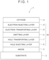
- FIG. 1 schematically shows an exemplary arrangement of the organic EL device according to the invention.
- An organic EL device 1 includes a light-transmissive substrate 2, an anode 3, a cathode 4, and an organic layer 10 provided between the anode 3 and the cathode 4.
- the organic layer 10 include a hole injecting layer 6, a hole transporting layer 7, an emitting layer 5, an electron transporting layer 8, and an electron injecting layer 9 which are laminated on the anode 3 in this order.
- the emitting layer of the organic EL device includes a first compound and a second compound.
- the emitting layer may contain a metal complex, but preferably contains no phosphorescent metal complex.
- the first compound is a thermally activated delayed fluorescent compound.
- An emission quantum efficiency of the first compound is 70% or less.
- the emission quantum efficiency of the first compound is preferably 65% or less, more preferably 60% or less.
- the emission quantum efficiency of the first compound is preferably more than 0%, more preferably 30% or more.
- the first compound is not a metal complex.
- the first compound is preferably represented by a formula (1).
- A is an acceptor moiety and is a group having a partial structure selected from partial structures represented by formulae (a-1) to (a-7). When a plurality of A are present, the plurality of A may be mutually the same or different and may be combined to form a saturated or unsaturated ring.
- B is a donor moiety and has one selected from partial structures represented by formulae (b-1) to (b-6). When a plurality of B are present, the plurality of B may be mutually the same or different and may be combined to form a saturated or unsaturated ring.
- a, b and d are each independently an integer from 1 to 5.
- c is an integer from 0 to 5.
- L is a linking group selected from the group consisting of a substituted or unsubstituted aromatic hydrocarbon group having 6 to 30 ring carbon atoms and a substituted or unsubstituted heterocyclic group having 5 to 30 ring atoms.
- the plurality of L may be mutually the same or different and may be combined to form a saturated or unsaturated ring.
- R is each independently a hydrogen atom or a substituent.
- the substituent is selected from the group consisting of a substituted or unsubstituted aromatic hydrocarbon group having 6 to 30 ring carbon atoms, a substituted or unsubstituted heterocyclic group having 5 to 30 ring atoms, and a substituted or unsubstituted alkyl group having 1 to 30 carbon atoms.
- the plurality of R may be mutually the same or different and may be combined to form a saturated or unsaturated ring.
- a bonding pattern of the compound represented by the formula (1) is exemplified by bonding patterns shown below in Table 1.
- Table 1 No. a b c d Bonding Pattern (1A) 1 1 0 1 B-A (1B) 1 1 1 1 B-L-A (1C) 2 1 0 1 B-A-A , (1D) 1 2 0 1 B-B-A , (1E) 2 1 1 1 B-L-A-A , (1F) 1 2 1 1 B-B-L-A , (1G) 1 1 2 1 B-L-L-A (1H) 1 1 1 2 B-L-B-L-A
- the first compound can be manufactured by a method described in International Publication No. WO2013/180241 , International Publication No. WO2014/092083 , International Publication No. WO2014/104346 and the like.
- Delayed fluorescence (thermally activated delayed fluorescence) is explained in " ADACHI, Chihaya, ed., "Yuki Hando-tai no Debaisu Bussei (Device Physics of Organic Semiconductors)", Kodansha, pp. 261-268 .”
- TADF thermally activated delayed fluorescence
- Fig. 10.38 in this literature illustrates an occurrence mechanism of the delayed fluorescence.
- the first compound is a compound exhibiting thermally activated delayed fluorescence caused by this mechanism. Occurrence of delayed fluorescence emission can be determined by transient PL (Photo Luminescence) measurement.
- the behavior of delayed fluorescence can be analyzed based on the decay curve obtained by the transient PL measurement.
- the transient PL measurement is a process where a sample is irradiated with a pulse laser to be excited, and a decay behavior (transient characteristics) of PL emission after the irradiation is stopped is measured.
- PL emission using a TADF material is divided into an emission component from singlet excitons generated by the first PL excitation and an emission component from singlet excitons generated via triplet excitons.
- the lifetime of the singlet excitons generated by the first PL excitation is in a nano-second order and considerably short. Emission from these singlet excitons thus decays immediately after the irradiation with the pulse laser.
- delayed fluorescence which is emission from the singlet excitons generated via long-life triplet excitons, decays slowly. There is thus a large difference in time between emission from the singlet excitons generated by the first PL excitation and emission from the singlet excitons generated via triplet excitons. Therefore, a luminous intensity resulting from the delayed fluorescence can be obtained.
- Fig. 2 schematically shows an exemplary device for measuring transient PL.
- a transient PL measuring device 100 includes: a pulse laser 101 capable of emitting light with a predetermined wavelength; a sample chamber 102 configured to house a measurement sample; a spectrometer 103 configured to disperse light emitted from the measurement sample; a streak camera 104 configured to form a two-dimensional image; and a personal computer 105 configured to analyze the two-dimensional image imported thereinto. It should be noted that transient PL may be measured by a device different from one described.
- the sample to be housed in the sample chamber 102 is prepared by forming a thin film, which is made of a matrix material doped with a doping material at a concentration of 12 mass%, on a quartz substrate.
- the thus-obtained thin film sample is housed in the sample chamber 102, and is irradiated with a pulse laser emitted from the pulse laser 101 to excite the doping material.
- the emitted excitation light is taken in a 90-degree direction with respect to the irradiation direction of the excitation light, and is dispersed by the spectrometer 103.
- a two-dimensional image of the light is formed through the streak camera 104.
- an ordinate axis corresponds to time
- an abscissa axis corresponds to wavelength
- a bright spot corresponds to luminous intensity.
- the two-dimensional image is taken at a predetermined time axis, thereby obtaining an emission spectrum with an ordinate axis representing luminous intensity and an abscissa axis representing wavelength. Further, the two-dimensional image is taken at a wavelength axis, thereby obtaining a decay curve (transient PL) with an ordinate axis representing the logarithm of luminous intensity and an abscissa axis representing time.
- transient PL decay curve
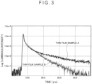
- a thin film sample A was prepared using a reference compound M1 below as a matrix material and a reference compound DP1 below as a doping material, and transient PL was measured.
- Respective decay curves of the thin film sample A and a thin film sample B were analyzed.
- the thin film sample B was prepared in the same manner as described above using a reference compound M2 below as a matrix material and the reference compound DP1 as a doping material.
- Fig. 3 shows a decay curve obtained from transient PL measured using each of the thin film samples A and B.
- an emission decay curve with an ordinate axis representing luminous intensity and an abscissa axis representing time can be obtained by the transient PL measurement. Based on the emission decay curve, a fluorescence intensity ratio between fluorescence emitted from a singlet state generated by photo-excitation and delayed fluorescence emitted from a singlet state generated by inverse energy transfer via a triplet state can be estimated. In a delayed fluorescent material, a ratio of the intensity of the slowly decaying delayed fluorescence to the intensity of the promptly decaying fluorescence is relatively large.
- the luminescence amount of the delayed fluorescence can be obtained using the device shown in Fig. 2 .
- Emission from the first compound includes: Prompt emission observed immediately when the excited state is achieved by exciting the first compound with a pulse beam (i.e., a beam emitted from a pulse laser) having an absorbable wavelength; and Delay emission observed not immediately when but after the excited state is achieved.
- the amount of Delay emission is preferably 5% or more relative to the amount of Prompt emission.
- the amount of Prompt emission and the amount of Delay emission can be obtained in the same method as a method described in " Nature 492, 234-238, 2012 .”
- the amount of Prompt emission and the amount of Delay emission may be calculated using a device different from one described in the above Literature.
- a sample usable for measuring the delayed fluorescence may be prepared by co-depositing the first compound and a compound TH-2 below on a quartz substrate at a ratio of the first compound being 12 mass% to form a 100-nm-thick thin film.
- the second compound is a fluorescent compound selected from the group consisting of a bisarylamino pyrene derivative, an aryl-substituted pyrene derivative, a bisarylamino chrysene derivative, an aryl-substituted chrysene derivative, a bisarylamino fluoranthene derivative, an aryl-substituted fluoranthene derivative, an indenoperylene derivative, a pyrromethene boron complex compound, a compound having a pyrromethene skeleton or a metal complex thereof, a diketopyrrolopyrrole derivative, and a perylene derivative.
- the second compound preferably emits fluorescence having a main peak wavelength (occasionally referred to as an emission peak wavelength) of 550 nm or less. Moreover, the second compound preferably emits fluorescence having the main peak wavelength of 430 nm or more.
- the main peak wavelength means a peak wavelength of luminescence spectrum exhibiting a maximum luminous intensity among luminous spectra measured using a toluene solution where the second compound is dissolved at a concentration from 10 -6 mol/l to 10 -5 mol/l.
- the second compound preferably emits a green or blue fluorescence.
- the second compound is preferably a material exhibiting a high emission quantum efficiency.
- the second compound may be a compound represented by a formula (10) below, in accordance with claim 1.
- a D is a substituted or unsubstituted aromatic hydrocarbon group having 12 to 50 ring carbon atoms.
- aromatic hydrocarbon group having 12 to 50 ring carbon atoms in A D include groups derived from naphthalene, anthracene, benzanthracene, phenanthrene, chrysene, pyrene, fluoranthene, benzofluoranthene, perylene, picene, triphenylene, fluorene, benzofluorene, stilbene and naphthacene, and further include benzo groups and ring-expanded groups of the aromatic hydrocarbon groups.
- B D is represented by a formula (11) below.
- pa is an integer of 1 to 4
- pb is an integer of 0 to 4.
- Ar 1 , Ar 2 and Ar 3 each independently represent a substituent selected from the group consisting of a substituted or unsubstituted aromatic hydrocarbon group having 6 to 50 ring carbon atoms, substituted or unsubstituted alkyl group having 1 to 50 carbon atoms, substituted or unsubstituted alkenyl group, substituted or unsubstituted alkynyl group, and substituted or unsubstituted heterocyclic group having 5 to 50 atoms forming a ring (i.e., ring atoms), and pc is an integer of 0 to 4.
- a wavy line in the formula (11) shows a bonding position with the aromatic hydrocarbon group represented by A D .
- a plurality of A D may be mutually the same or different
- a plurality of B D may be mutually the same or different
- a plurality of pa may be mutually the same or different
- a plurality of pb may be mutually the same or different
- a plurality of Ar 1 may be mutually the same or different
- a plurality of Ar 2 may be mutually the same or different
- a plurality of Ar 3 may be mutually the same or different
- a plurality of pc may be mutually the same or different.
- Examples of the compound represented by the formula (10) include the following compounds, but the second compound is not limited thereto.
- a D1 to A D4 each independently represent the same as A D
- B D1 to B D4 each independently represent the same as B D .
- the aromatic hydrocarbon group in A D is preferably an aromatic hydrocarbon group having 12 to 24 ring carbon atoms, more preferably an aromatic hydrocarbon group having 18 to 20 ring carbon atoms.
- Examples of the aromatic hydrocarbon group in A D includes a naphthylphenyl group, naphthyl group, acenaphthylenyl group, anthryl group, benzanthryl group, aceanthryl group, phenanthryl group, benzo[c]phenanthryl group, phenalenyl group, fluorenyl group, picenyl group, pentaphenyl group, pyrenyl group, chrysenyl group, benzo[g]chrysenyl group, s-indecenyl group, as-indecenyl group, fluoranthenyl group, benzo[k]fluoranthenyl group, triphenylenyl group, benzo[b]triphenylenyl group, benzoflu
- the aromatic hydrocarbon groups in Ar 1 , Ar 2 and Ar 3 are each independently an aromatic hydrocarbon group having 6 to 24 ring carbon atoms, more preferably an aromatic hydrocarbon group having 6 to 12 ring carbon atoms.
- the aromatic hydrocarbon groups in Ar 1 , Ar 2 and Ar 3 may each independently be any one of a phenyl group, naphthylphenyl group, biphenylyl group, terphenylyl group, naphthyl group, acenaphthylenyl group, anthryl group, benzoanthryl group, aceanthryl group, phenanthryl group, benzo[c]phenanthryl group, phenalenyl group, fluorenyl group, picenyl group, pentaphenyl group, pyrenyl group, chrysenyl group, benzo[g]chrysenyl group, s-indacenyl group, as-indacenyl group, fluoranthenyl group,
- Examples of the substituted aromatic hydrocarbon group include a phenylnaphthyl group, naphthylphenyl group, tolyl group, xylyl group, silylphenyl group, trimethylsilylphenyl group, 9,9-dimethylfluorenyl group, 9,9-diphenylfluorenyl group, 9,9'-spirobifluorenyl group and cyanophenyl group, among which, for instance, a tolyl group, xylyl group, trimethylsilylphenyl group, 9,9-dimethylfluorenyl group, 9,9-diphenylfluorenyl group, 9,9'-spirobifluorenyl group, cyanophenyl group and silylphenyl group are preferable.
- the alkyl group(s) in Ar 1 , Ar 2 and Ar 3 is preferably each independently an alkyl group having 1 to 10 carbon atoms, and more preferably an alkyl group having 1 to 5 carbon atoms.
- Examples of the alkyl group(s) in Ar 1 , Ar 2 and Ar 3 include a methyl group, ethyl group, n-propyl group, isopropyl group, n-butyl group, isobutyl group, s-butyl group, t-butyl group, pentyl group (including isomers thereof), hexyl group (including isomers thereof), heptyl group (including isomers thereof), octyl group (including isomers thereof), nonyl group (including isomers thereof), decyl group (including isomers thereof), undecyl group (including isomers thereof) and dodecyl group (including isomers thereof), among which a methyl group, ethyl group,
- the alkyl group(s) in Ar 1 , Ar 2 and Ar 3 may each independently be a cycloalkyl group having 3 to 50 ring carbon atoms.
- the cycloalkyl group(s) in Ar 1 , Ar 2 and Ar 3 is preferably each independently a cycloalkyl group having 3 to 6 ring carbon atoms, and more preferably a cycloalkyl group having 5 or 6 ring carbon atoms.
- Examples of the cycloalkyl group(s) in Ar 1 , Ar 2 and Ar 3 include a cyclopropyl group, cyclobutyl group, cyclopentyl group, cyclohexyl group, cycloheptyl group, cyclooctyl group and adamantyl group, among which a cyclopentyl group and cyclohexyl group are preferable.
- the alkenyl group(s) in Ar 1 , Ar 2 and Ar 3 is preferably each independently an alkenyl group having 2 to 20 carbon atoms, and more preferably an alkenyl group having 2 to 10 carbon atoms.
- Examples of the alkenyl group(s) in Ar 1 , Ar 2 and Ar 3 include a vinyl group, allyl group, 1-butenyl group, 2-butenyl group, 3-butenyl group, 1,3-butanedienyl group, 1-methylvinyl group, 1-methylallyl group, 1,1-dimethylallyl group, 2-methylallyl group and 1,2-dimethylallyl group.
- Examples of the substituted alkenyl group include a styryl group, 2,2-diphenylvinyl group, 1,2-diphenylvinyl group, 1-phenylallyl group, 2-phenylallyl group, 3-phenylallyl group, 3,3-diphenylallyl group, 1-phenyl-1-butenyl group and 3-phenyl-1-butenyl group.
- the alkynyl group(s) in Ar 1 , Ar 2 and Ar 3 is preferably each independently an alkynyl group having 2 to 20 carbon atoms, and more preferably an alkynyl group having 2 to 10 carbon atoms.
- the alkynyl group(s) in Ar 1 , Ar 2 and Ar 3 may be a propargyl group or a 3-pentynyl group.
- the heterocyclic group(s) in Ar 1 , Ar 2 and Ar 3 is preferably each independently a heterocyclic group having 5 to 24 ring atoms, and more preferably a heterocyclic group having 5 to 18 ring atoms.
- the heterocyclic group(s) in Ar 1 , Ar 2 and Ar 3 may be a heterocyclic group having 1 to 5 hetero atoms (e.g., nitrogen atom, oxygen atom and sulfur atom).
- the heterocyclic group(s) in Ar 1 , Ar 2 and Ar 3 may each independently be any one of a pyrrolyl group, furyl group, thienyl group, pyridyl group, pyridazynyl group, pyrimidinyl group, pyrazinyl group, triazinyl group, imidazolyl group, oxazolyl group, thiazolyl group, pyrazolyl group, isooxazolyl group, isothiazolyl group, oxadiazolyl group, thiadiazolyl group, triazolyl group, tetorazolyl group, indolyl group, isoindolyl group, benzofuranyl group, isobenzofuranyl group, benzothiophenyl group, isobenzothiophenyl group, indolizinyl group, quinolizinyl group, quinolyl group, isoquinolyl group, cinnolinyl
- Any substituent in a "substituted or unsubstituted" compound represented by the formula (10) is preferably selected from the group consisting of an alkyl group having 1 to 50 (preferably 1 to 10, more preferably 1 to 5) carbon atoms, an alkenyl group having 2 to 20 (preferably 2 to 10) carbon atoms, an alkynyl group having 2 to 20 (preferably 2 to 10) carbon atoms, a cycloalkyl having 3 to 50 (preferably 3 to 6, more preferably 5 or 6) ring carbon atoms, an aromatic hydrocarbon group having 6 to 50 (preferably 6 to 24, more preferably 6 to 12) ring carbon atoms, an aralkyl group having 1 to 50 (preferably 1 to 10, more preferably 1 to 5) carbon atoms containing an aromatic hydrocarbon group having 6 to 50 (preferably 6 to 24, more preferably 6 to 12) ring carbon atoms, an amino group, a monoalkylamino or dialkylamino group having an alkyl group having 1 to 50 (preferably 1
- a substituent selected from the group consisting of an alkyl group having 1 to 5 carbon atoms, cycloalkyl group having 5 or 6 carbon atoms, aromatic hydrocarbon group having 6 to 12 ring carbon atoms, and heterocyclic group having 5 to 24 ring atoms and 1 to 3 hetero atoms (a nitrogen atom, oxygen atom and sulfur atom) is particularly preferable.
- An alkyl group having 1 to 50 carbon atoms as a substituent in the substituted or unsubstituted group represents the same as those described as the alkyl group in Ar 1 , Ar 2 and Ar 3 .
- An alkenyl group having 2 to 20 carbon atoms as a substituent in the substituted or unsubstituted group represents the same as those described as the alkenyl group in Ar 1 , Ar 2 and Ar 3 .
- An alkynyl group having 2 to 20 carbon atoms as a substituent in the substituted or unsubstituted group represents the same as those described as the alkynyl group in Ar 1 , Ar 2 and Ar 3 .
- a cycloalkyl group having 3 to 50 ring carbon atoms as a substituent in the substituted or unsubstituted group represents the same as those described as the cycloalkyl group in Ar 1 , Ar 2 and Ar 3 .
- An aromatic hydrocarbon group having 6 to 50 ring carbon atoms as a substituent in the substituted or unsubstituted group represents the same as those described as the aromatic hydrocarbon group in Ar 1 , Ar 2 and Ar 3 .
- An aralkyl group having 6 to 50 ring carbon atoms as a substituent in the substituted or unsubstituted group includes an aromatic hydrocarbon group having 6 to 50 ring carbon atoms and an aralkyl group having 1 to 50 carbon atoms.
- Examples of an alkyl group moiety are the same as the above-described examples of the alkyl group.
- Examples of an aromatic hydrocarbon group moiety are the same as the above-described examples of the aromatic hydrocarbon group.
- examples of an alkyl group moiety are the same as the above-described examples of the alkyl group.
- examples of an aryl group (aromatic hydrocarbon group) moiety are the same as the above-described examples of the aromatic hydrocarbon group.
- alkoxy group as a substituent in the substituted or unsubstituted group
- examples of an alkyl group moiety are the same as the above-described examples of the alkyl group.
- the alkoxy group is preferably a methoxy group and an ethoxy group.
- an aryloxy group as a substituent in the substituted or unsubstituted group, examples of an aryl group (aromatic hydrocarbon group) moiety are the same as the above-described examples of the aromatic hydrocarbon group.
- the aryloxy group is exemplified by a phenoxy group.
- alkylthio group as a substituent in the substituted or unsubstituted group, examples of an alkyl group moiety are the same as the above-described examples of the alkyl group.
- an arylthio group as a substituent in the substituted or unsubstituted group, examples of an aryl group (aromatic hydrocarbon group) moiety are the same as the above-described examples of the aromatic hydrocarbon group.
- Examples of a mono-substituted silyl group, di-substituted silyl group or trisubstituted silyl group as a substituent in the substituted or unsubstituted group include an alkylsilyl group having 1 to 50 carbon atoms and an arylsilyl group having 6 to 50 ring carbon atoms.
- Examples of the alkylsilyl group having 1 to 50 carbon atoms include a monoalkylsilyl group, dialkylsilyl group and trialkylsilyl group. Specific examples of the alkyl group in each of those are the same as the above-described examples of the alkyl group.
- Examples of the arylsilyl group having 6 to 50 ring carbon atoms include a monoarylsilyl group, diarylsilyl group and triarylsilyl group.
- Specific examples of each aryl group in the arylsilyl group include a trimethylsilyl group, triethylsilyl group, t-butyldimethylsilyl group, vinyldimethylsilyl group, propyldimethylsilyl group, isopropyldimethylsilyl group, triphenylsilyl group, phenyldimethylsilyl group, t-butyldiphenylsilyl group and tritolylsilyl group.
- a heterocyclic group as a substituent in the substituted or unsubstituted group represents the same as those described as the aromatic heterocyclic group in Ar 1 , Ar 2 and Ar 3 .
- a haloalkyl group as a substituent in the substituted or unsubstituted group is exemplified by a group obtained by halogenating the above-described alkyl group, specifically, trifluoromethyl group.
- the organic EL device is capable of prolonging a lifetime, improving a luminous efficiency, and inhibiting a roll-off when driven at a high current density.
- the roll-off refers to a phenomenon in which a luminous efficiency is decreased when the organic EL device is driven at a high current density.
- the first compound contained in the emitting layer is a delayed fluorescent compound. Since the delayed fluorescent compound has a donor (electron-donating) moiety and an acceptor (electron accepting) moiety in a molecular structure, electric charges exist in a localized state in a molecule of the delayed fluorescent compound when the delayed fluorescent compound is excited. Since such a localized state of the electric charges possibly causes various side reactions, the delayed fluorescent compound having a long excited lifetime tends to exhibit a low stability especially in the excited state. Moreover, a half bandwidth of the luminescence spectrum of the delayed fluorescent compound is increased. Accordingly, it is difficult to use the delayed fluorescent compound as a luminescent material for a display unit requiring a high definition display in a large-sized TV set and the like.
- an organic EL device including an emitting layer containing a delayed fluorescent compound and a fluorescent compound has been studied.
- the delayed fluorescent compound is used as a sensitizer in the emitting layer and the fluorescent compound is used as the luminescent material.
- the fluorescent compound since the fluorescent compound emits light, it is expected that the half bandwidth of the luminescence spectrum is decreased.
- emission from the delayed fluorescent compound having a low excitation stability can be avoided, it is expected that a lifetime of the organic EL device is prolonged.
- it is theoretically expected that the same luminous efficiency as that of an organic EL device including an emitting layer containing a delayed fluorescent compound as a luminescent material is obtained.
- the inventors have found that a combination of the delayed fluorescent compound that is the first compound and the fluorescent compound that is the second compound under predetermined conditions can provide advantages of prolonging a lifetime, improving a luminous efficiency, and inhibiting a roll-off in a high current density region.
- An ionization potential Ip1 of the first compound and an ionization potential Ip2 of the second compound preferably satisfy a numerical formula below (Numerical Formula 1), further preferably satisfy a numerical formula below (Numerical Formula 1A).
- Ip1 and Ip2 preferably satisfy a numerical formula below (Numerical Formula 2).
- the numerical formula (Numerical Formula 2) is satisfied, the trap emission is easily inhibitable. 0 ⁇ Ip2 ⁇ Ip1 ⁇ 0.5 eV
- Ip2 -Ip1 > 0.8 eV the electrons are captured by the second compound to promote collision between the electrons and the excitons, thereby promoting the roll-off.
- Ip1 and Ip2 more preferably satisfy a numerical formula (Numerical Formula 2A). 0 ⁇ Ip2 ⁇ Ip1 ⁇ 0.5 eV
- the emission quantum efficiency of the first compound is not excessively small, and is preferably 30% or more.
- the emission quantum efficiency of the first compound exceeds 70%, the excited energy transfers to the second compound and the emission process from the first compound are likely to compete with each other. Accordingly, the emission quantum efficiency of the first compound is preferably 70% or less.
- the organic EL device preferably emits light exhibiting a peak in a wavelength range of 550 nm or less.
- the main peak wavelength of the light emitted from the organic EL device preferably falls within a range of 550 nm or less.
- the second compound mainly emits light in the emitting layer 5.
- the wavelength range of the light emitted by the organic EL device is more preferably from 430 nm to 550 nm.
- the organic EL device emits blue or green fluorescence.
- the first compound is preferably a compound having a small ⁇ ST(M1) so that inverse intersystem crossing from the triplet energy level of the first compound to the singlet energy level thereof is easily caused by a heat energy given from the outside.
- An energy state conversion mechanism to perform spin exchange from the triplet state of electrically excited excitons within the organic EL device to the singlet state by inverse intersystem crossing is referred to as a TADF mechanism.
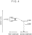
- Fig. 4 exemplarily shows a relationship in energy levels between the first compound and the second compound in the emitting layer.
- S0 represents a ground state
- S1(M1) represents a lowest singlet state of the first compound
- T1(M1) represents a lowest triplet state of the first compound
- S1(M2) represents a lowest singlet state of the second compound
- T1(M2) represents a lowest triplet state of the second compound.
- a dashed arrow directed from S1(M1) to S1(M2) in Fig. 4 represents Förster energy transfer from the lowest singlet state of the first compound to the lowest singlet state of the second compound.
- a difference between the lowest singlet state S1 and the lowest triplet state T1 is defined as ⁇ ST.
- a singlet energy S(M1) of the first compound is preferably larger than a singlet energy S(M2) of the second compound.
- An energy gap T 77K (M1) at 77[K] of the first compound is preferably larger than an energy gap T 77K (M2) at 77[K] of the second compound.
- T 77K (M1) is preferably 2.0 eV or more, more preferably 2.2 eV or more.
- the triplet energy is measured as follows. Firstly, a target compound for measurement is deposited on a quartz substrate to prepare a sample. Alternatively, the target compound is dissolved in an appropriate solvent to prepare a solution and the solution is encapsulated in a quartz glass pipe to prepare a sample. A phosphorescent spectrum (ordinate axis: phosphorescent luminous intensity, abscissa axis: wavelength) of the sample is measured at a low temperature (77K). A tangent is drawn to the rise of the phosphorescent spectrum on the short-wavelength side. The triplet energy is calculated by a predetermined conversion equation based on a wavelength value at an intersection of the tangent and the abscissa axis.
- the first compound is preferably a compound having a small ⁇ ST.
- ⁇ ST is small, intersystem crossing and inverse intersystem crossing are likely to occur even at a low temperature (77K), so that the singlet state and the triplet state coexist.
- the spectrum to be measured in the same manner as the above includes emission from both the singlet state and the triplet state.
- the value of the triplet energy is basically considered dominant.
- the triplet energy is measured by the same method as a typical triplet energy T, but a value measured in the following manner is referred to as an energy gap T 77K in order to differentiate the measured energy from the typical triplet energy in a strict meaning.
- the target compound for the measurement is deposited at a film thickness of 100 nm on a quartz substrate to form a sample.
- a phosphorescent spectrum (ordinate axis: phosphorescent luminous intensity, abscissa axis: wavelength) of the sample is measured at a low temperature (77K).
- a tangent is drawn to the rise of the phosphorescent spectrum on the short-wavelength side.
- An energy amount is calculated by the following conversion equation 1 based on a wavelength value ⁇ edge [nm] at an intersection of the tangent and the abscissa axis and defined as an energy gap T 77K .
- T 77 K eV 1239.85 / ⁇ dge
- the tangent to the rise of the phosphorescence spectrum on the short-wavelength side is drawn as follows. While moving on a curve of the phosphorescence spectrum from the short-wavelength side to the maximum spectral value closest to the short-wavelength side among the maximum spectral values, a tangent is checked at each point on the curve toward the long-wavelength of the phosphorescence spectrum. An inclination of the tangent is increased as the curve rises (i.e., a value of the ordinate axis is increased). A tangent drawn at a point of the maximum inclination (i.e., a tangent at an inflection point) was defined as the tangent to the rise of the phosphorescence spectrum on the short-wavelength side.
- the maximum with peak intensity being 15% or less of the maximum peak intensity of the spectrum is not included in the above-mentioned maximum closest to the short-wavelength side of the spectrum.
- the tangent drawn at a point of the maximum spectral value being closest to the short-wavelength side and having the maximum inclination is defined as a tangent to the rise of the phosphorescence spectrum on the short-wavelength side.
- a spectrophotofluorometer body F-4500 (manufactured by Hitachi High-Technologies Corporation) is usable.
- the measurement instrument is not limited to this arrangement.
- a combination of a cooling unit, a low temperature container, an excitation light source and a light-receiving unit may be used for measurement.
- the singlet energy S is measured as follows.
- Example 2 the absorption spectrum was measured using a spectrophotometer manufactured by Hitachi, Ltd. (device name: U3310). It should be noted that the absorption spectrum measuring device may be different from the above device.
- the tangent to the fall of the absorption spectrum on the long-wavelength side is drawn as follows. While moving on a curve of the absorption spectrum from the maximum spectral value closest to the long-wavelength side in a long-wavelength direction, a tangent at each point on the curve is checked. An inclination of the tangent is decreased and increased in a repeated manner as the curve falls (i.e., a value of the ordinate axis is decreased). A tangent drawn at a point of the minimum inclination closest to the long-wavelength side (except when absorbance is 0.1 or less) is defined as the tangent to the fall of the absorption spectrum on the long-wavelength side.
- the maximum absorbance of 0.2 or less is not included in the above-mentioned maximum absorbance on the long-wavelength side.
- a film thickness of the emitting layer 5 of the organic EL device 1 is preferably in a range from 5 nm to 100 nm, more preferably in a range from 7 nm to 100 nm, and most preferably in a range from 10 nm to 100 nm.
- the thickness of less than 5 nm may cause difficulty in forming the emitting layer 5 and in controlling chromaticity, while the thickness of more than 100 nm may raise drive voltage.
- a content ratio of the first compound is preferably 5 mass% or more, more preferably in a range from 10 mass% to 80 mass%, further preferably in a range from 40 mass% to 60 mass%.
- a content ratio of the second compound is preferably in a range from 1 mass% to 10 mass%.
- An upper limit of the total of the respective content ratios of the first and second compounds in the emitting layer 5 is 100 mass%. It should be noted that the emitting layer 5 further contain another material in addition to the first and second compounds.
- a substrate 2 is used as a support for the organic EL device 1.
- glass, quartz, plastics and the like are usable as the substrate 2.
- a flexible substrate is also usable.
- the flexible substrate is a bendable substrate.
- the flexible substrate is exemplified by a plastic substrate formed of polycarbonate, polyarylate, polyethersulfone, polypropylene, polyester, polyvinyl fluoride, polyvinyl chloride, polyimide, polyethylene naphthalate or the like.
- an inorganic vapor deposition film is also usable as the substrate 2.
- Metal, alloy, an electrically conductive compound, a mixture thereof and the like, which have a large work function (specifically, of 4.0 eV or more) is preferably usable as the anode 3 formed on the substrate 2.
- the material for the anode include indium tin oxide (ITO), indium tin oxide containing silicon or silicon oxide, indium zinc oxide, tungsten oxide, indium oxide containing zinc oxide and graphene.
- gold Au
- platinum Pt
- nickel Ni
- tungsten W
- chrome Cr
- molybdenum Mo
- iron Fe
- cobalt Co
- copper Cu
- palladium Pd
- titanium Ti
- nitrides of a metal material e.g., titanium nitride
- indium zinc oxide can be deposited as a film by sputtering using a target that is obtained by adding zinc oxide in a range from 1 mass% to 10 mass% to indium oxide.
- indium oxide containing tungsten oxide and zinc oxide can be deposited as a film by sputtering using a target that is obtained by adding tungsten oxide in a range from 0.5 mass% to 5 mass% and zinc oxide in a range from 0.1 mass% to 1 mass% to indium oxide.
- vapor deposition, coating, ink jet printing, spin coating and the like may be used for forming the anode 3.
- a hole injecting layer 6 formed adjacent to the anode 3 is formed of a composite material that facilitates injection of holes irrespective of the work function of the anode 3. Accordingly, a material usable as an electrode material (e.g., metal, alloy, an electrically conductive compound, a mixture thereof, and elements belonging to Groups 1 and 2 of the periodic table of the elements) is usable as the material for the anode 3.
- an electrode material e.g., metal, alloy, an electrically conductive compound, a mixture thereof, and elements belonging to Groups 1 and 2 of the periodic table of the elements
- the elements belonging to Groups 1 and 2 of the periodic table of the elements which are materials having a small work function, namely, an alkali metal such as lithium (Li) and cesium (Cs) and an alkaline earth metal such as magnesium (Mg), calcium (Ca) and strontium (Sr), alloy thereof (e.g., MgAg, AlLi), a rare earth metal such as europium (Eu) and ytterbium (Yb), and alloy thereof are also usable as the material for the anode.
- an alkali metal such as lithium (Li) and cesium (Cs)
- an alkaline earth metal such as magnesium (Mg), calcium (Ca) and strontium (Sr), alloy thereof (e.g., MgAg, AlLi)
- a rare earth metal such as europium (Eu) and ytterbium (Yb)
- alloy thereof e.g., MgAg, AlLi
- a rare earth metal such as euro
- a hole injecting layer 6 is a layer containing a highly hole-injectable substance.
- the highly hole-injectable substance include molybdenum oxide, titanium oxide, vanadium oxide, rhenium oxide, ruthenium oxide, chromium oxide, zirconium oxide, hafnium oxide, tantalum oxide, silver oxide, tungsten oxide, and manganese oxide.
- the examples of the highly hole-injectable substance further include: an aromatic amine compound, which is a low-molecule compound, such that 4,4',4"-tris(N,N-diphenylamino)triphenylamine (abbreviation: TDATA), 4,4',4"-tris[N-(3-methylphenyl)-N-phenylamino]triphenylamine (abbreviation: MTDATA), 4,4'-bis[N-(4-diphenylaminophenyl)-N-phenylamino]biphenyl(abbreviation: DPAB), 4,4'-bis(N- ⁇ 4-[N'-(3-methylphenyl)-N'-phenylamino]phenyl ⁇ -N-phenylamino)biphenyl (abbreviation: DNTPD), 1,3,5-tris[N-(4-diphenylaminophenyl)-N-phenylamino]benzene (abbreviation:
- a high-molecule compound e.g., an oligomer, dendrimer and polymer
- the high-molecule compound include poly(N-vinylcarbazole) (abbreviation: PVK), poly(4-vinyltriphenylamine) (abbreviation: PVTPA), poly[N-(4- ⁇ N'-[4-(4-diphenylamino)phenyl]phenyl-N'-phenylamino ⁇ phenyl)methacrylamido] (abbreviation: PTPDMA), and poly[N,N'-bis(4-butylphenyl)-N,N'-bis(phenyl)benzidine] (abbreviation: Poly-TPD).
- PVK poly(N-vinylcarbazole)
- PVTPA poly(4-vinyltriphenylamine)
- PTPDMA poly[N-(4- ⁇ N'-[4-(4-diphenylamino)phenyl]phen
- the examples of the high-molecule compound include a high-molecule compound added with an acid such as poly(3,4-ethylene dioxythiophene)/poly(styrene sulfonic acid) (PEDOT/PSS), and polyaniline/poly(styrene sulfonic acid) (PAni/PSS).
- an acid such as poly(3,4-ethylene dioxythiophene)/poly(styrene sulfonic acid) (PEDOT/PSS), and polyaniline/poly(styrene sulfonic acid) (PAni/PSS).
- a hole transporting layer 7 is a layer containing a highly hole-transportable substance.
- An aromatic amine compound, carbazole derivative, anthracene derivative and the like are usable for the hole transporting layer 7.
- Specific examples of a material for the hole transporting layer 7 include 4,4'-bis[N-(1-naphthyl)-N-phenylamino]biphenyl (abbreviation: NPB), N,N'-bis(3-methylphenyl)-N,N'-diphenyl-[1,1'-biphenyl]-4,4'-diamine (abbreviation: TPD), 4-phenyl-4'-(9-phenylfluorene-9-yl)triphenylamine (abbreviation: BAFLP), 4,4'-bis[N-(9,9-dimethylfluorene-2-yl)-N-phenylamino]biphenyl (abbreviation: DFLDPBi), 4,4
- a carbazole derivative such as CBP, 9-[4-(N-carbazolyl)]phenyl-10-phenyl anthracene (CzPA) and 9-phenyl-3-[4-(10-phenyl-9-anthryl)phenyl]-9H-carbazole (PCzPA); an anthracene derivative such as t-BuDNA, DNA, and DPAnth; and a high-molecular weight compound such as poly(N-vinylcarbazole)(abbreviation: PVK) and poly(4-vinyltriphenylamine)(abbreviation: PVTPA) are usable for the hole transporting layer 7.
- CBP 9-[4-(N-carbazolyl)]phenyl-10-phenyl anthracene
- PCzPA 9-phenyl-3-[4-(10-phenyl-9-anthryl)phenyl]-9H-carbazole
- an anthracene derivative such as
- a highly hole-transportable substance may be provided in the form of a single layer or a laminated layer of two or more layers of the above substance.
- the hole transporting layer includes two or more layers
- one of the layers with a larger energy gap is preferably provided closer to the emitting layer 5.
- the hole transporting layer 7 preferably has a function of preventing triplet excitons generated in the emitting layer 5 from diffusing into the hole transporting layer to trap the triplet excitons within the emitting layer 5.
- An electron transporting layer 8 is a layer containing a highly electron-transportable substance.
- a metal complex such as an aluminum complex, beryllium complex and zinc complex
- heteroaromatic compound such as an imidazole derivative, benzimidazole derivative, azine derivative, carbazole derivative, and phenanthroline derivative
- 3) a high-molecule compound are usable.
- a metal complex such as Alq, tris(4-methyl-8-quinolinato)aluminum (abbreviation: Almq3), bis(10-hydroxybenzo[h]quinolinato)beryllium (abbreviation: BeBq2), BAlq, Znq, ZnPBO and ZnBTZ are usable.
- a heteroaromatic compound such as 2-(4-biphenyl)-5-(4-tert-butylphenyl)-1,3,4-oxadiazole (abbreviation: PBD), 1,3-bis[5-(ptert-butylphenyl)-1,3,4-oxadiazole-2-yl]benzene (abbreviation: OXD-7), 3-(4-tert-butylphenyl)-4-phenyl-5-(4-biphenyl)-1,2,4-triazole (abbreviation: TAZ), 3-(4-tert-butylphenyl)-4-(4-ethylphenyl)-5-(4-biphenyl)-1,2,4-triazole (abbreviation: p-EtTAZ), bathophenanthroline (abbreviation: BPhen), bathocuproine (abbreviation: BCP), and 4,4'-bis(5-methyl
- a benzimidazole compound is suitably usable.
- the above-described substances mostly have an electron mobility of 10 -6 cm 2 /(V•s) or more.
- any substance having an electron transporting performance higher than a hole transporting performance may be used for the electron transporting layer 8 in addition to the above substances.
- the electron transporting layer 8 may be provided in the form of a single layer or a laminated layer of two or more layers of the above substance(s).
- a high-molecule compound is also usable for the electron transporting layer 8.
- poly[(9,9-dihexylfluorene-2,7-diyl)-co-(pyridine-3,5-diyl)] (abbreviation: PF-Py)
- poly[(9,9-dioctylfluorene-2,7-diyl)-co-(2,2'-bipyridine-6,6'-diyl)] abbreviation: PF-BPy
- PF-BPy poly[(9,9-dioctylfluorene-2,7-diyl)-co-(2,2'-bipyridine-6,6'-diyl)]
- the hole transporting layer 8 preferably has a function of preventing triplet excitons generated in the emitting layer 5 from diffusing into the hole transporting layer 8 and the electron injecting layer 9 to trap the triplet excitons within the emitting layer 5.
- An electron injecting layer 9 is a layer containing a highly electron-injectable substance.
- a material for the electron injecting layer include an alkali metal, alkaline earth metal and a compound thereof, examples of which include lithium (Li), cesium (Cs), calcium (Ca), lithium fluoride (LiF), cesium fluoride (CsF), calcium fluoride (CaF2), and lithium oxide (LiOx).
- a substance obtained by containing an alkali metal, alkaline earth metal or a compound thereof in the electron transportable substance specifically, for instance, a substance obtained by containing magnesium (Mg) in Alq may be used. With this substance, electrons can be more efficiently injected from the cathode 4.
- a composite material provided by mixing an organic compound with an electron donor may be used for the electron injecting layer 9.
- the composite material exhibits excellent electron injecting performance and electron transporting performance since the electron donor generates electron in the organic compound.
- the organic compound is preferably a material exhibiting an excellent transforming performance of the generated electrons.
- the above-described substance for the electron transporting layer 8 e.g., the metal complex and heteroaromatic compound
- the electron donor may be any substance exhibiting an electron donating performance to the organic compound.
- an alkali metal, alkaline earth metal and a rare earth metal are preferable, examples of which include lithium, cesium, magnesium, calcium, erbium and ytterbium.
- an alkali metal oxide and alkaline earth metal oxide are preferable, examples of which include lithium oxide, calcium oxide, and barium oxide.
- Lewis base such as magnesium oxide is also usable.
- tetrathiafulvalene (abbreviation: TTF) is also usable.
- Metal, alloy, an electrically conductive compound, a mixture thereof and the like, which have a small work function, specifically, of 3.8 eV or less, is preferably usable as a material for the cathode 4.
- the material for the cathode 4 include: the elements belonging to Groups 1 and 2 of the periodic table of the elements, namely, an alkali metal such as litium (Li) and cesium (Cs) and an alkaline earth metal such as magnesium (Mg), calcium (Ca) and strontium (Sr); alloy thereof (e.g., MgAg, AlLi); a rare earth metal such as europium (Eu) and ytterbium (Yb); and alloy thereof.
- an alkali metal such as litium (Li) and cesium (Cs) and an alkaline earth metal such as magnesium (Mg), calcium (Ca) and strontium (Sr)
- alloy thereof e.g., MgAg, AlLi
- a rare earth metal
- the cathode 4 When the cathode 4 is formed of the alkali metal, alkaline earth metal and alloy thereof, vapor deposition and sputtering are usable. Moreover, when the cathode 4 is formed of silver paste and the like, coating, ink jet printing and the like are usable.
- various conductive materials such as Al, Ag, ITO, graphene and indium tin oxide containing silicon or silicon oxide are usable for forming the cathode 4 irrespective of the magnitude of the work function.
- the conductive materials can be deposited as a film by sputtering, inkjet printing, spin coating and the like.
- each layer of the organic EL device There is no restriction except for the above particular description for a method for forming each layer of the organic EL device 1.
- Known methods such as dry film-forming and wet film-forming are applicable.
- the dry film-forming include vacuum deposition, sputtering, plasma and ion plating.
- the wet film-forming include spin coating, dipping, flow coating and ink-jet printing.
- the film thickness is typically preferably in a range of several nanometers to 1 ⁇ m because an excessively-thinned film is likely to cause defects such as a pin hole while an excessively-thickened film requires high voltage to be applied and deteriorates efficiency.
- the number of carbon atoms forming a ring means the number of carbon atoms included in atoms forming the ring itself of a compound in which the atoms are bonded to form the ring (e.g., a monocyclic compound, a fused ring compound, a cross-linked compound, a carbocyclic compound, and a heterocyclic compound).
- a monocyclic compound, a fused ring compound, a cross-linked compound, a carbocyclic compound, and a heterocyclic compound e.g., a monocyclic compound, a fused ring compound, a cross-linked compound, a carbocyclic compound, and a heterocyclic compound.
- the "ring carbon atoms" do not include carbon(s) contained in the substituent. Unless specifically described, the same applies to the "ring carbon atoms" described later.
- a benzene ring has 6 ring carbon atoms
- a naphthalene ring has 10 ring carbon atoms
- a pyridinyl group has 5 ring carbon atoms
- a furanyl group has 4 ring carbon atoms.
- the benzene ring and/or the naphthalene ring is substituted by, for instance, an alkyl group
- the number of carbon atoms of the alkyl group is not included in the number of the ring carbon atoms.
- a fluorene ring When a fluorene ring is substituted by, for instance, a fluorene ring (e.g., a spirofluorene ring), the number of carbon atoms of the fluorene ring as a substituent is not counted in the number of the ring carbon atoms for the fluorene ring.
- a fluorene ring e.g., a spirofluorene ring
- the number of atoms forming a ring means the number of atoms forming the ring itself of a compound in which the atoms are bonded to form the ring (e.g., a monocyclic compound, a fused ring compound, a cross-linked compound, a carbocyclic compound, and a heterocyclic compound).
- Atom(s) not forming the ring e.g., a hydrogen atom for terminating the atoms forming the ring
- atoms included in a substituent substituting the ring are not counted in the number of the ring atoms. Unless specifically described, the same applies to the "ring atoms" described later.
- a pyridine ring has 6 ring atoms
- a quinazoline ring has 10 ring atoms
- a furan ring has 5 ring atoms.
- Hydrogen atoms respectively bonded to the pyridine ring and the quinazoline ring and atoms forming the substituents are not counted in the number of the ring atoms.
- a fluorene ring is substituted by, for instance, a fluorene ring (e.g., a spirofluorene ring)
- the number of atoms of the fluorene ring as a substituent is not included in the number of the ring atoms for the fluorene ring.
- Examples of the aromatic hydrocarbon group (occasionally referred to as an aryl group) having 6 to 30 ring carbon atoms or 6 to 40 ring carbon atoms herein include a phenyl group, biphenyl group, terphenyl group, naphthyl group, anthryl group, phenanthryl group, fluorenyl group, pyrenyl group, chrysenyl group, fluoranthenyl group, benz[a]anthryl group, benzo[c]phenanthryl group, triphenylenyl group, benzo[k]fluoranthenyl group, benzo[g]chrysenyl group, benzo[b]triphenylenyl group, picenyl group, and perylenyl group.
- the aryl group herein preferably has 6 to 20 ring carbon atoms, more preferably 6 to 14 ring carbon atoms, further preferably 6 to 12 ring carbon atoms.
- a phenyl group, biphenyl group, naphthyl group, phenanthryl group, terphenyl group and fluorenyl group are particularly preferable.
- a carbon atom at a position 9 of each of 1-fluorenyl group, 2-fluorenyl group, 3-fluorenyl group and 4-fluorenyl group is preferably substituted by a substituted or unsubstituted alkyl group having 1 to 30 carbon atoms or a substituted or unsubstituted aryl group having 6 to 18 ring carbon atoms later described herein.
- the heterocyclic group (occasionally, referred to as heteroaryl group, heteroaromatic ring group or aromatic heterocyclic group) having 5 to 30 ring atoms herein preferably contains at least one atom selected from the group consisting of nitrogen, sulfur, oxygen, silicon, selenium atom and germanium atom, and more preferably contains at least one atom selected from the group consisting of nitrogen, sulfur and oxygen.
- heterocyclic group (occasionally, referred to as heteroaryl group, heteroaromatic ring group or aromatic heterocyclic group) having 5 to 30 ring atoms herein include a pyridyl group, pyrimidinyl group, pyrazinyl group, pyridazynyl group, triazinyl group, quinolyl group, isoquinolinyl group, naphthyridinyl group, phthalazinyl group, quinoxalinyl group, quinazolinyl group, phenanthridinyl group, acridinyl group, phenanthrolinyl group, pyrrolyl group, imidazolyl group, pyrazolyl group, triazolyl group, tetrazolyl group, indolyl group, benzimidazolyl group, indazolyl group, imidazopyridinyl group, benzotriazolyl group, carbazolyl group, furyl group,
- the heterocyclic group herein preferably has 5 to 20 ring atoms, more preferably 5 to 14 ring atoms.
- a 1-dibenzofuranyl group, 2-dibenzofuranyl group, 3-dibenzofuranyl group, 4-dibenzofuranyl group, 1-dibenzothiophenyl group, 2-dibenzothiophenyl group, 3-dibenzothiophenyl group, 4-dibenzothiophenyl group, 1-carbazolyl group, 2-carbazolyl group, 3-carbazolyl group, 4-carbazolyl group, and 9-carbazolyl group are particularly preferable.
- a nitrogen atom at a position 9 of each of 1-carbazolyl group, 2-carbazolyl group, 3-carbazolyl group and 4-carbazolyl group is preferably substituted by a substituted or unsubstituted aryl group having 6 to 30 ring carbon atoms or a substituted or unsubstituted heterocyclic group having 5 to 30 ring atoms herein.
- heterocyclic group may be a group derived from any one of partial structures represented by formulae (XY-1) to (XY-18).
- X and Y each independently represent a hetero atom, and preferably represent an oxygen atom, sulfur atom, selenium atom, silicon atom or germanium atom.
- the partial structures represented by the formulae (XY-1) to (XY-18) may each be bonded in any position to be a heterocyclic group, which may be substituted.
- examples of the substituted or unsubstituted carbazolyl group may include a group in which a carbazole ring is further fused with a ring(s) as shown in the following formulae. Such a group may be substituted. The group may be bonded in any position as desired.
- the alkyl group having 1 to 30 carbon atoms herein may be linear, branched or cyclic.
- Examples of the linear or branched alkyl group are a methyl group, ethyl group, propyl group, isopropyl group, n-butyl group, s-butyl group, isobutyl group, t-butyl group, n-pentyl group, n-hexyl group, n-heptyl group, n-octyl group, n-nonyl group, n-decyl group, n-undecyl group, n-dodecyl group, n-tridecyl group, n-tetradecyl group, n-pentadecyl group, n-hexadecyl group, n-heptadecyl group, n-octadecyl group, neo-pentyl group
- the linear or branched alkyl group herein preferably has 1 to 10 carbon atoms, more preferably 1 to 6 carbon atoms.
- a methyl group, ethyl group, propyl group, isopropyl group, n-butyl group, s-butyl group, isobutyl group, t-butyl group, n-pentyl group, n-hexyl group, amyl group, isoamyl group and neopentyl group are particularly preferable.
- Examples of the cycloalkyl group having 3 to 30 carbon atoms herein are a cyclopropyl group, cyclobutyl group, cyclopentyl group, cyclohexyl group, 4-metylcyclohexyl group, adamantyl group and norbornyl group.
- the cycloalkyl group preferably has 3 to 10 ring carbon atoms, more preferably 5 to 8 ring carbon atoms.
- a cyclopentyl group and a cyclohexyl group are particularly preferable.
- a halogenated alkyl group provided by substituting an alkyl group with a halogen atom is exemplified by one provided by substituting an alkyl group having 1 to 30 carbon atoms with one or more halogen groups.
- Specific examples of the above halogenated alkyl group are a fluoromethyl group, difluoromethyl group, trifluoromethyl group, fluoroethyl group, trifluoromethylmethyl group, trifluoroethyl group and pentafluoroethyl group.
- carbon atoms forming a ring mean carbon atoms forming a saturated ring, unsaturated ring, or aromatic ring.
- “Atoms forming a ring (ring atoms)” mean carbon atoms and hetero atoms forming a hetero ring including a saturated ring, unsaturated ring, or aromatic ring.
- a “hydrogen atom” means isotopes having different neutron numbers and specifically encompasses protium, deuterium and tritium.
- examples of the substituent meant by "substituted or unsubstituted” include an aralkyl group, substituted amino group, halogen atom, cyano group, alkoxy group, aryloxy group, alkylsilyl group, arylsilyl group, alkenyl group, alkynyl group, alkylthio group, arylthio group, hydroxyl group, nitro group, and carboxy group.
- an aryl group, heterocyclic group, alkyl group, halogen atom, alkylsilyl group, arylsilyl group and cyano group are preferable. More preferable substituents are one listed as the preferable substituents described for each substituent.
- the above substituents may be further substituted by at least one group selected from the group consisting of an aryl group, heterocyclic group, alkyl group , alkylsilyl group, arylsilyl group, alkoxy group, aryloxy group, alkylamino group, arylamino group, alkylthio group, arylthio group, alkenyl group, alkynyl group, aralkyl group, halogen atom, cyano group, hydroxyl group, nitro group, and carboxy group.
- plural ones of these substituents may be mutually bonded to form a ring.
- the alkoxy group having 1 to 30 carbon atoms is represented by -OZi.
- Z 1 is exemplified by the above alkyl group having 1 to 30 carbon atoms.
- Examples of the alkoxy group are a methoxy group, ethoxy group, propoxy group, butoxy group, pentyloxy group and hexyloxy group.
- the alkoxy group preferably has 1 to 20 carbon atoms.
- a halogenated alkoxy group provided by substituting an alkoxy group with a halogen atom is exemplified by one provided by substituting an alkoxy group having 1 to 30 carbon atoms with one or more halogen groups.
- the aryloxy group having 6 to 30 ring carbon atoms is represented by-OZ 2 .
- Z 2 is exemplified by the above aryl group having 6 to 30 ring carbon atoms.
- the aryloxy group preferably has 6 to 20 ring carbon atoms.
- the aryloxy group is exemplified by a phenoxy group.
- substituted amino group examples include an alkylamino group having 2 to 30 carbon atoms and an arylamino group having 6 to 60 ring carbon atoms.
- the alkylamino group having 2 to 30 carbon atoms is represented by -NHRv or - N(R V ) 2 .
- R V is exemplified by the alkyl group having 1 to 30 carbon atoms.
- the arylamino group having 6 to 60 ring carbon atoms is represented by -NHRw or -N(R W ) 2 .
- R W is exemplified by the above aryl group having 6 to 30 ring carbon atoms.
- halogen atom examples include a fluorine atom, chlorine atom, bromine tom and iodine atom, among which a fluorine atom is preferable.
- the aralkyl group is preferably an aralkyl group having 6 to 30 ring carbon atoms and is represented by -Z 3 -Z 4 .
- Z 3 is exemplified by an alkylene group corresponding to the above alkyl group having 1 to 30 carbon atoms.
- Z 4 is exemplified by the above aryl group having 6 to 30 ring carbon atoms.
- This aralkyl group is preferably an aralkyl group having 7 to 30 carbon atoms, in which an aryl moiety has 6 to 30 carbon atoms, preferably 6 to 20 carbon atoms, more preferably 6 to 12 carbon atoms and an alkyl moiety has 1 to 30 carbon atoms, preferably 1 to 20 carbon atoms, more preferably 1 to 10 carbon atoms, further preferably 1 to 6 carbon atoms.
- Examples of the aralkyl group include a benzyl group, 2-phenylpropane-2-yl group, 1-phenylethyl group, 2-phenylethyl group, 1-phenylisopropyl group, 2-phenylisopropyl group, phenyl-t-butyl group, ⁇ -naphthylmethyl group, 1- ⁇ -naphthylethyl group, 2- ⁇ -naphthylethyl group, 1- ⁇ -naphthylisopropyl group, 2- ⁇ -naphthylisopropyl group, ⁇ -naphthylmethyl group, 1- ⁇ -naphthylethyl group, 2- ⁇ -naphthylethyl group, 1- ⁇ -naphthylisopropyl group, and 2- ⁇ -naphthylisopropyl group.
- the alkenyl group is preferably an alkenyl group having 2 to 30 carbon atoms, which may be linear, branched or cyclic.
- Examples of the alkenyl group include a vinyl group, propenyl group, butenyl group, oleyl group, eicosapentaenyl group, docosahexaenyl group, styryl group, 2,2-diphenylvinyl group, 1,2,2-triphenylvinyl group, 2-phenyl-2-propenyl group, cyclopentadienyl group, cyclopentenyl group, cyclohexenyl group, and cyclohexadienyl group.
- the alkynyl group is preferably an alkynyl group having 2 to 30 carbon atoms, which may be linear, branched or cyclic.
- Examples of the alkynyl group include ethynyl, propynyl, and 2-phenylethynyl.
- the alkylthio group having 1 to 30 carbon atoms is represented by -SRv.
- Rv is exemplified by the alkyl group having 1 to 30 carbon atoms.
- the alkylthio group preferably has 1 to 20 carbon atoms.
- the arylthio group having 6 to 30 ring carbon atoms is represented by -SR W .
- R W is exemplified by the above aryl group having 6 to 30 ring carbon atoms.
- the arylthio group preferably has 6 to 20 ring carbon atoms.
- Examples of the substituted silyl group include an alkylsilyl group having 3 to 30 carbon atoms and an arylsilyl group having 6 to 30 ring carbon atoms.
- the alkylsilyl group having 3 to 30 carbon atoms herein is exemplified by an alkylsilyl group having the alkyl group listed as the examples of the alkyl group having 1 to 30 carbon atoms.
- examples of the alkylsilyl group are a trimethylsilyl group, a triethylsilyl group, a tri-n-butylsilyl group, a tri-n-octylsilyl group, a triisobutyl silyl group, a dimethylethylsilyl group, a dimethylisopropylsilyl group, a dimethyl-n-propylsilyl group, a dimethyl-n-butylsilyl group, a dimethyl-t-butylsilyl group, a diethylisopropylsilyl group, a vinyldimethylsilyl group, a propyldimethylsilyl group and triisopropyl si
- arylsilyl group having 6 to 30 ring carbon atoms examples are a dialkylarylsilyl group, alkyldiarylsilyl group and triarylsilyl group.
- the dialkylarylsilyl group is exemplified by a dialkylarylsilyl group including two of the alkyl group listed as the examples of the alkyl group having 1 to 30 carbon atoms and one of the aryl group listed as the examples of the aryl group having 6 to 30 ring carbon atoms.
- the dialkylarylsilyl group preferably has 8 to 30 carbon atoms.
- the alkyldiarylsilyl group is exemplified by an alkyldiarylsilyl group including one of the alkyl group listed as the examples of the alkyl group having 1 to 30 carbon atoms and two of the aryl group listed as the examples of the aryl group having 6 to 30 ring carbon atoms.
- the alkyldiarylsilyl group preferably has 13 to 30 carbon atoms.
- the triarylsilyl group is exemplified by a triarylsilyl group including three of the aryl group listed as the examples of the aryl group having 6 to 30 ring carbon atoms.
- the triarylsilyl group preferably has 18 to 30 carbon atoms.
- An aldehyde group, carbonyl group, ester group, carbamoyl group, and amino group may be substituted by an aliphatic hydrocarbon, alicyclic hydrocarbon, aromatic hydrocarbon, or heterocycle.
- the aliphatic hydrocarbon, alicyclic hydrocarbon, aromatic hydrocarbon, and heterocycle may further have a substituent.
- a siloxanyl group is a silicon compound group with an ether bond and is exemplified by a trimethylsiloxanyl group.
- XX to YY carbon atoms in the description of "substituted or unsubstituted ZZ group having XX to YY carbon atoms” represent carbon atoms of an unsubstituted ZZ group and do not include carbon atoms of a substituent(s) of the substituted ZZ group.
- YY is larger than “XX.”
- XX and YY each mean an integer of 1 or more.
- XX to YY atoms in the description of "substituted or unsubstituted ZZ group having XX to YY atoms” represent atoms of an unsubstituted ZZ group and does not include atoms of a substituent(s) of the substituted ZZ group.
- YY is larger than “XX.”
- XX and YY each mean an integer of 1 or more.
- the ring structure is a saturated ring, unsaturated ring, aromatic hydrocarbon ring, or a heterocycle.
- the ring structure formed by bonding the substituents may have a substituent.
- examples of the aromatic hydrocarbon group and the heterocyclic group in the linking group include divalent groups obtained by eliminating one hydrogen atom from the above monovalent groups.
- examples of the aromatic hydrocarbon ring and the heterocycle include ring structures from which the above monovalent groups are derived.
- the organic EL device 1 is usable in an electronic device such as a display unit and a light-emitting unit.
- the display unit include display components such as an organic EL panel module, TV, mobile phone, tablet, and personal computer.
- Examples of the light-emitting unit include an illuminator and a vehicle light.
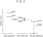
- the organic EL device according to the invention further includes a third compound in the emitting layer.
- a singlet energy of the third compound is larger than the singlet energy of the first compound.
- Fig. 5 exemplarily shows a relationship in energy levels between the first compound, the second compound and the third compound in the emitting layer.
- S0 represents a ground state
- S1(M1) represents the lowest singlet state of the first compound
- T1(M1) represents the lowest triplet state of the first compound
- S1(M2) represents the lowest singlet state of the second compound
- T1(M2) represents the lowest triplet state of the second compound
- S1(M3) represents a lowest singlet state of the third compound
- T1(M3) represents a lowest triplet state of the third compound.
- a dashed arrow directed from S1(M1) to S1(M2) in Fig. 5 represents Förster energy transfer from the lowest singlet state of the first compound to the lowest singlet state of the second compound.
- the content ratio of the first compound is in a range from 10 mass% to 80 mass%
- the content ratio of the second compound is in a range from 1 mass% to 10 mass%
- the content ratio of the third compound is in a range from 10 mass% to 80 mass%.
- the content ratio of the first compound is more preferably in a range from 20 mass% to 80 mass%, further preferably in a range from 40 mass% to 60 mass%.
- An upper limit of the total of the respective content ratios of the first to third compounds in the emitting layer is 100 mass%. It should be noted that the emitting layer may further contain another material in addition to the first to third compounds.
- the third compound is not particularly limited, the third compound is preferably a compound other than an amine compound.
- the third compound is preferably a compound other than an amine compound.
- a carbazole derivative, dibenzofuran derivative and dibenzothiophene derivative are usable as the third compound.
- the third compound is not limited thereto.
- the third compound preferably has at least one of a partial structure represented by a formula (31) below and a partial structure represented by a formula (32) below in one molecule.
- Y 31 to Y 36 each independently represent a nitrogen atom or a carbon atom bonded to another atom in the molecule of the third compound.
- At least one of Y 31 to Y 36 is a carbon atom bonded to another atom in the molecule of the third compound.
- Y 41 to Y 48 each independently represent a nitrogen atom or a carbon atom bonded to another atom in the molecule of the third compound.
- At least one of Y 41 to Y 48 is a carbon atom bonded to another atom in the molecule of the third compound.
- X 3 represents a nitrogen atom, an oxygen atom or a sulfur atom.
- Y 41 to Y 48 are carbon atoms bonded to another atom in the molecule of the third compound and a ring structure is formed including the carbon atoms.
- the partial structure represented by the formula (32) is preferably a partial structure selected from the group consisting of formulae (321), (322), (323), (324), (325) and (326) below.
- X 3 represents a nitrogen atom, an oxygen atom or a sulfur atom.
- Y 41 to Y 48 each independently represent a nitrogen atom or a carbon atom bonded to another atom in the molecule of the third compound.
- X 4 represents a nitrogen atom, an oxygen atom, a sulfur atom or a carbon atom.
- Y 51 to Y 54 each independently represent a nitrogen atom or a carbon atom bonded to another atom in the molecule of the third compound.
- the third compound preferably contains the partial structure represented by the formula (323) among the formulae (321) to (326).
- the partial structure represented by the formula (31) is preferably in the form of at least one group selected from the group consisting of groups represented by formulae (33) and (34) below and contained in the third compound.
- bonding positions are preferably both situated in meta positions as shown in the formulae (33) and (34) to keep an energy gap T 77K (M3) at 77 [K] high.
- Y 31 , Y 32 , Y 34 and Y 36 each independently represent a nitrogen atom or CR 31 , in which R 31 represents a hydrogen atom or a substituent.
- R 31 represents a hydrogen atom or a substituent.
- the substituent is selected from the group consisting of a substituted or unsubstituted aromatic hydrocarbon group having 6 to 30 ring carbon atoms, a substituted or unsubstituted heterocyclic group having 5 to 30 ring atoms, a substituted or unsubstituted alkyl group having 1 to 30 carbon atoms, a substituted or unsubstituted fluoroalkyl group having 1 to 30 carbon atoms, a substituted or unsubstituted cycloalkyl group having 3 to 30 carbon atoms, a substituted or unsubstituted aralkyl group having 7 to 30 carbon atoms, a substituted silyl group, a substituted germanium group, a substituted pho
- Wavy lines in the formulae (33) and (34) each show a bonding position with another atom or another structure in the molecule of the third compound.
- Y 31 , Y 32 , Y 34 and Y 36 are preferably each independently CR 31 .
- a plurality of R 31 may be the same or different.
- Y 32 , Y 34 and Y 36 are preferably each independently CR 31 .
- a plurality of R 31 may be the same or different.
- the substituted germanium group is preferably represented by -Ge(R 101 ) 3 .
- R 101 are each independently a substituent.
- the substituent R 101 is preferably a substituted or unsubstituted alkyl group having 1 to 30 carbon atoms or a substituted or unsubstituted aromatic hydrocarbon group having 6 to 30 ring carbon atoms.
- the plurality of R 101 may be mutually the same or different
- the partial structure represented by the formula (32) is preferably in the form of at least one group selected from the group consisting of groups respectively represented by formulae (35), (36), (37), (38), (39) and (30a) below and contained in the third compound.
- Y 41 , Y 42 , Y 43 , Y 44 , Y 45 , Y 46 , Y 47 and Y 48 each independently represent a nitrogen atom or CR 32 .
- R 32 represents a hydrogen atom or a substituent.
- the substituent is selected from the group consisting of a substituted or unsubstituted aromatic hydrocarbon group having 6 to 30 ring carbon atoms, a substituted or unsubstituted heterocyclic group having 5 to 30 ring atoms, a substituted or unsubstituted alkyl group having 1 to 30 carbon atoms, a substituted or unsubstituted fluoroalkyl group having 1 to 30 carbon atoms, a substituted or unsubstituted cycloalkyl group having 3 to 30 carbon atoms, a substituted or unsubstituted aralkyl group having 7 to 30 carbon atoms, a substituted silyl group, a substituted germanium group, a substituted phosphine oxide group, a halogen atom, a cyano group, a nitro group, and a carboxy group.
- X 3 in the formulae (35) and (36) represents a nitrogen atom.
- X 3 in the formulae (37) to (39) and (30a) represents NR 33 , an oxygen atom or a sulfur atom.
- R 33 is a substituent selected from the group consisting of a substituted or unsubstituted aromatic hydrocarbon group having 6 to 30 ring carbon atoms, a substituted or unsubstituted heterocyclic group having 5 to 30 ring atoms, a substituted or unsubstituted alkyl group having 1 to 30 carbon atoms, a substituted or unsubstituted fluoroalkyl group having 1 to 30 carbon atoms, a substituted or unsubstituted cycloalkyl group having 3 to 30 carbon atoms, a substituted or unsubstituted aralkyl group having 7 to 30 carbon atoms, a substituted silyl group, a substituted germanium group, a substituted phosphine oxide group, a fluorine atom, a cyano group, a nitro group, and a carboxy group.
- Wavy lines in the formulae (35) to (39) and (30a) each show a bonding position with another atom or another structure in the molecule of the third compound.
- Y 41 to Y 48 are preferably each independently CR 32 .
- Y 41 to Y 45 , Y 47 and Y 48 are preferably each independently CR 32 .
- Y 41 , Y 42 , Y 44 , Y 45 , Y 47 and Y 48 are preferably each independently CR 32 .
- Y 42 to Y 48 are preferably each independently CR 32 .
- Y 42 to Y 47 are preferably each independently CR 32 .
- a plurality of R 32 may be the same or different.
- X 3 is preferably an oxygen atom or a sulfur atom, more preferably an oxygen atom.
- R 31 and R 32 each independently represent a hydrogen atom or a substituent.
- the substituent in R 31 and R 32 is preferably selected from the group consisting of a fluorine atom, a cyano group, a substituted or unsubstituted alkyl group having 1 to 30 carbon atoms, a substituted or unsubstituted aromatic hydrocarbon group having 6 to 30 ring carbon atoms, and a substituted or unsubstituted heterocyclic group having 5 to 30 ring atoms.
- R 31 and R 32 are a hydrogen atom, a cyano group, a substituted or unsubstituted aromatic hydrocarbon group having 6 to 30 ring carbon atoms, or a substituted or unsubstituted heterocyclic group having 5 to 30 ring atoms.
- the substituted or unsubstituted aromatic hydrocarbon group having 6 to 30 ring carbon atoms in R 31 and R 32 is preferably a non-fused ring.
- the third compound is also preferably an aromatic hydrocarbon compound or an aromatic heterocyclic compound. It is also preferable that the third compound has no fused aromatic hydrocarbon ring in a molecule.
- the third compound may be prepared by a method described in International Publications WO2012/153780 , WO2013/038650 and the like.
- aromatic hydrocarbon group (occasionally referred to as an aryl group) include a phenyl group, tolyl group, xylyl group, naphthyl group, phenanthryl group, pyrenyl group, chrysenyl group, benzo[c]phenanthryl group, benzo[g]chrysenyl group, benzoanthryl group, triphenylenyl group, fluorenyl group, 9,9-dimethylfluorenyl group, benzofluorenyl group, dibenzofluorenyl group, biphenyl group, terphenyl group, quarterphenyl group and fluoranthenyl group, among which a phenyl group, biphenyl group, terphenyl group, quarterphenyl group, naphthyl group, triphenylenyl group and fluorenyl group may be preferable.
- substituted aromatic hydrocarbon group examples include a tolyl group, xylyl group and 9,9-dimethylfluorenyl group.
- the aryl group includes both fused aryl group and non-fused aryl group.
- aromatic hydrocarbon group examples include a phenyl group, biphenyl group, terphenyl group, quarterphenyl group, naphthyl group, triphenylenyl group and fluorenyl group.
- aromatic heterocyclic group (occasionally referred to as a heteroaryl group, heteroaromatic ring group or heterocyclic group) include a pyrrolyl group, pyrazolyl group, pyrazinyl group, pyrimidinyl group, pyridazynyl group, pyridyl group, triazinyl group, indolyl group, isoindolyl group, imidazolyl group, benzimidazolyl group, indazolyl group, imidazo[1,2-a]pyridinyl group, furyl group, benzofuranyl group, isobenzofuranyl group, dibenzofuranyl group, azadibenzofuranyl group, thiophenyl group, benzothiophenyl group, dibenzothiophenyl group, azadibenzothiophenyl group, quinolyl group, isoquinolyl group, quinoxalinyl group, quinazoliny
- the aromatic heterocyclic group is preferably any one of a dibenzofuranyl group, dibenzothiophenyl group, carbazolyl group, pyridyl group, pyrimidinyl group, triazinyl group, azadibenzofuranyl group and azadibenzothiophenyl group, and further preferably any one of a dibenzofuranyl group, dibenzothiophenyl group, azadibenzofuranyl group and azadibenzothiophenyl group.
- the substituted silyl group is also preferably a substituted or unsubstituted trialkylsilyl group, a substituted or unsubstituted arylalkylsilyl group, or a substituted or unsubstituted triarylsilyl group.
- substituted or unsubstituted trialkylsilyl group examples include a trimethylsilyl group and a triethysilyl group.
- substituted or unsubstituted arylalkylsilyl group examples include a diphenylmethylsilyl group, ditolylmethylsilyl group, and phenyldimethylsilyl group.
- substituted or unsubstituted triarylsilyl group examples include a triphenylsilyl group and a tritolylsilyl group.
- the substituted phosphine oxide group is also preferably a substituted or unsubstituted diarylphosphine oxide group.
- substituted or unsubstituted diarylphosphine oxide group examples include a diphenylphosphine oxide group and ditolylphosphine oxide group.
- the organic EL device is capable of prolonging a lifetime, improving a luminous efficiency, and inhibiting a roll-off when driven at a high current density.
- the emitting layer of the organic EL device includes the delayed fluorescent first compound, the fluorescent second compound, and the third compound having a larger singlet energy than the first compound, whereby the luminous efficiency of the organic EL device is further improved. It is deduced that the luminous efficiency is improved because a carrier balance in the emitting layer is improved by containing the third compound.
- the invention is not limited to the exemplary embodiment.
- the invention may include any modification and improvement compatible with the invention.
- the emitting layer is not limited to a single layer, but may be provided by laminating a plurality of emitting layers.
- the organic EL device has the plurality of emitting layers, it is only required that at least one of the emitting layers contains the first and second compounds.
- the rest of the emitting layers may be a fluorescent emitting layer or a phosphorescent emitting layer with use of emission caused by electron transfer from the triplet state directly to the ground state.
- the organic EL device includes the plurality of emitting layers
- the plurality of emitting layers may be adjacent to each other, or provide a so-called tandem-type organic EL device in which a plurality of emitting units are layered through an intermediate layer.
- a blocking layer may be provided in contact with an anode-side or a cathode-side of the emitting layer.
- the blocking layer is preferably provided in contact with the emitting layer to block at least ones of holes, electrons and excitons.
- the blocking layer when the blocking layer is provided in contact with the cathode-side of the emitting layer, the blocking layer permits transport of electrons, but prevents holes from reaching a layer provided near the cathode (e.g., the electron transporting layer) beyond the blocking layer.
- the blocking layer is preferably interposed between the emitting layer and the electron transporting layer.
- the blocking layer When the blocking layer is provided in contact with the anode-side of the emitting layer, the blocking layer permits transport of holes, but prevents electrons from reaching a layer provided near the anode (e.g., the hole transporting layer) beyond the blocking layer.
- the blocking layer is preferably interposed between the emitting layer and the hole transporting layer.
- the blocking layer may be provided in contact with the emitting layer to prevent an excitation energy from leaking from the emitting layer into a layer in the vicinity thereof.
- Excitons generated in the emitting layer are prevented from moving into a layer provided near the electrode (e.g., the electron transporting layer and the hole transporting layer) beyond the blocking layer.
- the emitting layer and the blocking layer are preferably bonded to each other.
- a photoelectron spectroscopy device (AC-3, manufactured by Riken Keiki Co., Ltd.) was used for the measurement of an ionization potential under atmosphere. Specifically, a compound to be measured was irradiated with light and the amount of electrons generated by charge separation was measured.
- a sample i.e., measurement target
- the prepared sample solution was put into a 1-cm cell.
- An absorption spectrum of the cell was measured using an absorptiometer.
- An excitation wavelength in the luminescence spectrum measurement was determined based on the measured absorption spectrum. It should be noted that the excitation wavelength is desirably a wavelength providing an absorption peak, but not limited thereto.
- a concentration of the sample solution is desirably weak to inhibit the emission from being re-absorbed. In the present measurement, the concentration of the sample solution was prepared such that an absorbance in the excitation wavelength was 0.05 or less.
- the sample solution as prepared above was put into a glass sample pipe provided with a vacuum stopcock.
- This sample pipe was connected to a vacuum line provided with a vacuum pump and a vacuum gauge and was subjected to freeze-deaeration.
- the freeze-deaeration in the present measurement refers to an operation in which a solution-accumulating portion of the sample pipe is soaked in liquid nitrogen to freeze the sample solution and an inside of the sample pipe is vacuumized.
- a rotary pump was used as the vacuum pump and a pirani vacuum gauge was used as the vacuum gauge. It should be noted that the vacuum pump and the vacuum gauge are not limited to the vacuum pump and the vacuum gauge used in the present measurement.
- the sample solution was dissolved at the room temperature and was again subjected to the freeze-deaeration. This operation was repeated until no change in the vacuum degree was observed.
- the solution obtained as a result of the repeated operation was defined as a deaeration sample solution.
- the sample pipe containing the deaeration sample solution and a 1-cm lidded cell were put into a glove box. Under inactive gas (e.g., nitrogen) atmosphere in the glove box, the deaeration sample solution was transferred from the sample pipe to the lidded cell and the lidded cell was hermetically sealed. After hermetically sealed, the lidded cell was taken out of the glove box.
- a luminescence spectrum of the deaeration sample solution was measured using a fluorometer. A line connecting a rise of the obtained luminescence spectrum on a short-wavelength side and a rise thereof on a long-wavelength side was defined as a reference line and an area intensity F 1 of the emission was calculated.
- ⁇ 2 represents an emission quantum efficiency of the standard sample
- a 1 represents an absorbance of the sample solution in the excitation wavelength
- a 2 represents an absorbance of the standard sample solution in the excitation wavelength
- n 1 represents a refractive index of a solvent used for preparing the sample solution
- n 2 represents a refractive index of a solvent used for preparing the standard sample solution.
- An absorptiometer (device name: UV-3100PC) manufactured by Shimadzu Corporation was used as an absorption spectrum measurement device.
- a fluorometer (device name: F-4500) manufactured by Hitachi, Ltd. was used as a luminescence spectrum measurement device.
- the standard sample solution is not particularly limited to the solution used in the present measurement as long as having the known emission quantum efficiency.
- the solvent is not limited to the solvent used in the present measurement.
- the absorption spectrum measuring device and the luminescence spectrum measurement device are not limited to the above devices used in the present measurement.
- Occurrence of delayed fluorescence emission was determined by measuring transient photoluminescence (PL) using a device shown in Fig. 2 .
- a sample was prepared by co-depositing the compounds H-1 and TH-2 on a quartz substrate at a ratio of the compound H-1 being 12 mass% to form a 100-nm-thick thin film.
- Emission from the compound H-1 include: Prompt emission observed immediately when the excited state is achieved by exciting the compound H-1 with a pulse beam (i.e., a beam emitted from a pulse laser) having an absorbable wavelength; and Delay emission observed not immediately when but after the excited state is achieved. Delayed fluorescence emission means that the amount of Delay emission is 5% or more relative to the amount of Prompt emission.
- the amount of Delay emission of the compound H-1 is 5% or more relative to the amount of Prompt emission.
- the amount of Prompt emission and the amount of Delay emission can be obtained in the same method as a method described in " Nature 492, 234-238, 2012 .”
- the amount of Prompt emission and the amount of Delay emission may be calculated using a device different from ones shown in Fig. 2 and described in Reference Literatures.
- Example 2 the absorption spectrum was measured using a spectrophotometer manufactured by Hitachi, Ltd. (device name: U3310). It should be noted that the absorption spectrum measuring device may be different from the above device.
- the calculated singlet energy S is shown below.
- the organic EL devices were prepared in the following manner and evaluated.
- a glass substrate (size: 25 mm ⁇ 75 mm ⁇ 1.1 mm thick, manufactured by Geomatec Co., Ltd.) having an ITO transparent electrode (anode) was ultrasonic-cleaned in isopropyl alcohol for five minutes, and then UV/ozone-cleaned for 30 minutes.
- a film of ITO was 130 nm thick.
- the glass substrate having the transparent electrode line was cleaned, the glass substrate was mounted on a substrate holder of a vacuum evaporation apparatus. Initially, a compound HI was deposited on a surface of the glass substrate where the transparent electrode line was provided in a manner to cover the transparent electrode, thereby forming a 5-nm-thick hole injecting layer.
- a compound HT-1 was deposited on the hole injecting layer to form a 110-nm-thick first hole transporting layer on the HI film.
- a compound HT-2 was deposited on the first hole transporting layer to form a 15-nm-thick second hole transporting layer.
- a compound DA, the compound H-1 and a compound D-1 were codeposited on the second hole transporting layer to form a 25-nm-thick emitting layer.
- a concentration of the compound H-1 was set to be 50 mass% and a concentration of the compound D-1 was set to be 1 mass%.
- a compound HB-1 was deposited on the emitting layer to form a 5-nm-thick hole blocking layer.
- a compound ET-1 was deposited on the hole blocking layer to form a 35-nm-thick electron transporting layer.
- LiF Lithium fluoride
- a metal aluminum (Al) was then deposited on the electron injecting electrode to form an 80-nm-thick metal Al cathode.
- a device arrangement of the organic EL device in Example 1 is schematically shown as follows.
- An organic EL device of Comparative 1 was manufactured in the same manner as the organic EL device of Example 1 except that a compound D-2 was used in place of the compound D-1 in the emitting layer of Example 1.
- a device arrangement of the organic EL device of Comparative 1 is roughly shown as follows.
- An organic EL device of Comparative 2 was manufactured in the same manner as the organic EL device of Example 1 except that a compound D-3 was used in place of the compound D-1 in the emitting layer of Example 1.
- a device arrangement of the organic EL device of Comparative 2 is roughly shown as follows.
- An organic EL device of Comparative 3 was manufactured in the same manner as the organic EL device of Example 1 except that the compound H-2 was used in place of the compound H-1 in the emitting layer of Example 1.
- a device arrangement of the organic EL device of Comparative 3 is roughly shown as follows.
- An organic EL device of Comparative 4 was manufactured in the same manner as the organic EL device of Comparative 3 except that the compound D-2 was used in place of the compound D-1 in the emitting layer of Comparative 3.
- a device arrangement of the organic EL device of Comparative 4 is roughly shown as follows.
- An organic EL device of Comparative 5 was manufactured in the same manner as the organic EL device of Comparative 3 except that the compound D-3 was used in place of the compound D-1 in the emitting layer of Comparative 3.
- a device arrangement of the organic EL device of Comparative 5 is roughly shown as follows.
- a main peak wavelength ⁇ p was calculated based on the obtained spectral-radiance spectra.
- An initial current density was set at 50 mA/cm 2 and a continuous current test was performed. A time elapsed until a luminance intensity was reduced to 80% of an initial luminance intensity at the start of the test was defined as a lifetime (LT80).
- Each of the organic EL devices of Example 1 and Comparatives 1, 3 and 4 was driven under the driving conditions of the current densities at 0.1 mA/cm 2 , 1 mA/cm 2 and 10 mA/cm 2 .
- a ratio of the external quantum efficiency under each of the driving conditions relative to the highest external quantum efficiency among the obtained external quantum efficiencies was calculated.
- the organic EL device of Example 1 exhibited a higher external quantum efficiency and a longer lifetime and inhibited roll-off when driven at a high current density.
Landscapes
- Chemical & Material Sciences (AREA)
- Engineering & Computer Science (AREA)
- Materials Engineering (AREA)
- Physics & Mathematics (AREA)
- Spectroscopy & Molecular Physics (AREA)
- Organic Chemistry (AREA)
- Optics & Photonics (AREA)
- Inorganic Chemistry (AREA)
- Electroluminescent Light Sources (AREA)
Claims (13)
- Un dispositif électroluminescent organique comprenant:une anode (3);une couche émettrice (5); etune cathode (4), dans lequella couche émettrice comprend un premier composé et un deuxième composé,le premier composé est un composé fluorescent retardé activé thermiquement,le deuxième composé est un composé fluorescent, dans lequel ledit deuxième composé est choisi dans le groupe constitué d'un dérivé de pyrène bisarylamino, d'un dérivé de pyrène substitué par un aryle, d'un dérivé de chrysène bisarylamino, d'un dérivé de chrysène substitué par un aryle, un dérivé de fluoranthène bisarylamino, un dérivé de fluoranthène substitué par un aryle, un dérivé d'indénopérylène, un composé complexe de pyrrométhène et de bore, un composé ayant un squelette de pyrrométhène ou un complexe métallique de celui-ci, un dérivé de dicétopyrrolopyrrole et un dérivé de pérylène,une efficacité quantique d'émission du premier composé est 70% ou moins, ladite efficacité quantique d'émission est déterminée comme décrit dans la spécification, etun potentiel d'ionisation Ip1 du premier composé et un péotentiel d'ionisation Ip2 du deuxième composé satisfont à une relation de
 la couche émettrice comprend en outre un troisième composé, etune énergie singulet du troisième composé est supérieure à une énergie singulet du premier composé.
 - Le dispositif électroluminescent organique selon la revendication 1, dans lequel
le potentiel d'ionisation Ip1 du premier composé et le potentiel d'ionisation Ip2 du deuxième composé satisfont à la relation suivante
- Le dispositif électroluminescent organique selon l'une des revendications 1 à 2, dans lequel l'efficacité quantique d'émission du premier composé est 65% ou moins.
- Le dispositif électroluminescent organique selon l'une des revendications 1 à 2, dans lequel l'efficacité quantique d'émission du premier composé est 60 % ou moin.
- Le dispositif électroluminescent organique selon l'une des revendications 1 à 4, dans lequel l'efficacité quantique d'émission du premier composé est 30% ou plus.
- Le dispositif électroluminescent organique selon l'une des revendications 1 à 5, dans lequel l'énergie singulet du premier composé est supérieure à l'énergie singulet du deuxième composé.
- Le dispositif électroluminescent organique selon l'une des revendications 1 à 6, dans lequel le deuxième composé a une longueur d'onde du pic d'émission de 550 nm ou moins.
- Le dispositif électroluminescent organique selon l'une des revendications 1 à 7, dans lequel le deuxième composé émet une fluorescence bleue.
- Le dispositif électroluminescent organique selon l'une des revendications 1 à 8, dans lequel le rapport de teneur du premier composé dans la couche émettrice est compris dans une plage de 10 % en masse à 80 % en masse.
- Le dispositif électroluminescent organique selon l'une des revendications 1 à 9, dans lequel un rapport de teneur du premier composé dans la couche émettrice est compris dans une plage allant de 40 % en masse à 60 % en masse.
- Le dispositif électroluminescent organique selon l'une des revendications 1 à 10, comprenant en outre: une couche de transport de trous entre l'anode et la couche émettrice.
- Le dispositif électroluminescent organique selon l'une des revendications 1 à 11, comprenant en outre: une couche de transport d'électrons entre la couche émettrice et la cathode.
- Un dispositif électronique comprenant le dispositif électroluminescent organique selon l'une des revendications 1 à 12.
Applications Claiming Priority (2)
| Application Number | Priority Date | Filing Date | Title |
|---|---|---|---|
| JP2015022731 | 2015-02-06 | ||
| PCT/JP2016/053109 WO2016125807A1 (fr) | 2015-02-06 | 2016-02-02 | Élément électroluminescent organique et dispositif électronique |
Publications (3)
| Publication Number | Publication Date |
|---|---|
| EP3255693A1 EP3255693A1 (fr) | 2017-12-13 |
| EP3255693A4 EP3255693A4 (fr) | 2018-10-03 |
| EP3255693B1 true EP3255693B1 (fr) | 2024-10-09 |
Family
ID=56564147
Family Applications (1)
| Application Number | Title | Priority Date | Filing Date |
|---|---|---|---|
| EP16746638.2A Active EP3255693B1 (fr) | 2015-02-06 | 2016-02-02 | Élément électroluminescent organique et dispositif électronique |
Country Status (7)
| Country | Link |
|---|---|
| US (2) | US10125310B2 (fr) |
| EP (1) | EP3255693B1 (fr) |
| JP (1) | JP6663363B2 (fr) |
| KR (1) | KR102660767B1 (fr) |
| CN (1) | CN107112431B (fr) |
| TW (1) | TWI726865B (fr) |
| WO (1) | WO2016125807A1 (fr) |
Families Citing this family (12)
| Publication number | Priority date | Publication date | Assignee | Title |
|---|---|---|---|---|
| WO2017038728A1 (fr) | 2015-08-28 | 2017-03-09 | 出光興産株式会社 | Composé, matériau d'élément électroluminescent organique, élément électroluminescent organique et dispositif électronique |
| JP2019204805A (ja) * | 2016-08-10 | 2019-11-28 | 出光興産株式会社 | 有機エレクトロルミネッセンス素子、及び電子機器 |
| US20210151683A1 (en) * | 2017-07-10 | 2021-05-20 | Toray Industries, Inc. | Light-emitting element, and display, illuminator, and sensor each including same |
| JP2021177443A (ja) * | 2018-05-28 | 2021-11-11 | 出光興産株式会社 | 有機エレクトロルミネッセンス素子、表示装置及び電子機器 |
| EP3587423A1 (fr) | 2018-06-27 | 2020-01-01 | Idemitsu Kosan Co., Ltd. | Composés organiques et dispositif électroluminescent organique les comprenant |
| KR102769406B1 (ko) * | 2018-09-12 | 2025-02-17 | 메르크 파텐트 게엠베하 | 유기 전계발광 디바이스용 재료 |
| EP3651225A1 (fr) | 2018-11-09 | 2020-05-13 | Idemitsu Kosan Co., Ltd. | Nouveaux composés organiques et dispositif électroluminescent organique les comprenant |
| US10784458B1 (en) * | 2019-03-15 | 2020-09-22 | Yuan Ze University | Organic light-emitting diode with enhanced light-emitting efficiency and color purity |
| JP2022137315A (ja) * | 2019-05-27 | 2022-09-22 | 出光興産株式会社 | 有機エレクトロルミネッセンス素子及び電子機器 |
| CN110911575B (zh) * | 2019-11-29 | 2023-04-07 | 昆山国显光电有限公司 | 一种有机电致发光器件及显示装置 |
| JP2022112591A (ja) * | 2021-01-22 | 2022-08-03 | キヤノン株式会社 | 有機発光素子、表示装置、撮像装置、電子機器、照明装置及び移動体 |
| JP2023004428A (ja) * | 2021-06-25 | 2023-01-17 | 出光興産株式会社 | 有機エレクトロルミネッセンス素子、有機エレクトロルミネッセンス表示装置及び電子機器 |
Citations (1)
| Publication number | Priority date | Publication date | Assignee | Title |
|---|---|---|---|---|
| WO2014157619A1 (fr) * | 2013-03-29 | 2014-10-02 | 国立大学法人九州大学 | Élément électroluminescent organique |
Family Cites Families (26)
| Publication number | Priority date | Publication date | Assignee | Title |
|---|---|---|---|---|
| EP1502936A1 (fr) * | 2002-03-25 | 2005-02-02 | Idemitsu Kosan Co., Ltd. | Materiau pour element organique electroluminescent et element organique electroluminescent l'utilisant |
| US7368178B2 (en) * | 2004-01-08 | 2008-05-06 | Eastman Kodak Company | Stable organic light-emitting devices using aminoanthracenes |
| TWI552406B (zh) * | 2011-03-25 | 2016-10-01 | 出光興產股份有限公司 | 有機電致發光元件 |
| JPWO2012153780A1 (ja) | 2011-05-11 | 2014-07-31 | 出光興産株式会社 | 新規化合物、有機エレクトロルミネッセンス素子用材料及び有機エレクトロルミネッセンス素子 |
| EP2709183B1 (fr) * | 2011-05-13 | 2019-02-06 | Joled Inc. | Dispositif électroluminescent organique d'émission de lumière à couleurs multiples |
| US9978952B2 (en) | 2011-09-13 | 2018-05-22 | Idemitsu Kosan Co., Ltd. | Fused heterocyclic aromatic derivative, organic electroluminescence element material, and organic electroluminescence element using same |
| JP5594750B2 (ja) * | 2012-05-17 | 2014-09-24 | 国立大学法人九州大学 | 化合物、発光材料および有機発光素子 |
| WO2013180241A1 (fr) | 2012-06-01 | 2013-12-05 | 出光興産株式会社 | Élément à électroluminescence organique et matériel pour un élément à électroluminescence organique |
| JP6187080B2 (ja) * | 2012-10-11 | 2017-08-30 | Tdk株式会社 | 電界発光素子 |
| US10297761B2 (en) | 2012-12-10 | 2019-05-21 | Idemitsu Kosan Co., Ltd. | Organic electroluminescent element |
| WO2014104346A1 (fr) | 2012-12-28 | 2014-07-03 | 出光興産株式会社 | Élément électroluminescent organique |
| WO2014157610A1 (fr) * | 2013-03-29 | 2014-10-02 | コニカミノルタ株式会社 | Elément électroluminescent organique, dispositif d'éclairage, dispositif d'affichage, couche mince électroluminescente et composition pour élément électroluminescent organique, et procédé d'électroluminescence |
| JP6567498B2 (ja) * | 2013-04-08 | 2019-08-28 | メルク パテント ゲーエムベーハー | 熱活性化遅延蛍光材料をもつ有機エレクトロルミネッセント素子 |
| US20160181545A1 (en) * | 2013-06-06 | 2016-06-23 | Merck Patent Gmbh | Organic electroluminescent device |
| CN105340101B (zh) * | 2013-07-03 | 2017-03-15 | 九州有机光材股份有限公司 | 发光材料、延迟萤光体、有机发光元件及化合物 |
| JP6573442B2 (ja) * | 2013-07-30 | 2019-09-11 | 出光興産株式会社 | 有機エレクトロルミネッセンス素子および電子機器 |
| KR102543775B1 (ko) * | 2013-08-14 | 2023-06-14 | 가부시키가이샤 큐럭스 | 유기 일렉트로루미네선스 소자 |
| JP6088995B2 (ja) * | 2013-10-24 | 2017-03-01 | 出光興産株式会社 | 有機エレクトロルミネッセンス素子および電子機器 |
| JP6522313B2 (ja) * | 2013-10-24 | 2019-05-29 | 出光興産株式会社 | 有機エレクトロルミネッセンス素子および電子機器 |
| JP5905916B2 (ja) * | 2013-12-26 | 2016-04-20 | 出光興産株式会社 | 有機エレクトロルミネッセンス素子および電子機器 |
| JP6827808B2 (ja) | 2014-07-31 | 2021-02-10 | コニカミノルタ株式会社 | 有機エレクトロルミネッセンス素子、発光性薄膜、表示装置及び照明装置 |
| JP6673203B2 (ja) | 2014-07-31 | 2020-03-25 | コニカミノルタ株式会社 | 有機エレクトロルミネッセンス素子 |
| WO2016017684A1 (fr) | 2014-07-31 | 2016-02-04 | コニカミノルタ株式会社 | Matériau d'élément électroluminescent organique, élément électroluminescent organique, film mince émettant de la lumière, dispositif d'affichage et dispositif d'éclairage |
| WO2016017514A1 (fr) | 2014-07-31 | 2016-02-04 | コニカミノルタ株式会社 | Élément électroluminescent organique, film mince émetteur de lumière, dispositif d'affichage et dispositif d'éclairage |
| WO2016017741A1 (fr) | 2014-07-31 | 2016-02-04 | コニカミノルタ株式会社 | Élément électroluminescent organique, dispositif d'affichage, dispositif d'éclairage, composé émetteur de lumière fluorescente, et film mince émetteur de lumière |
| US10340470B2 (en) * | 2016-02-23 | 2019-07-02 | Semiconductor Energy Laboratory Co., Ltd. | Light-emitting element, display device, electronic device, and lighting apparatus |
-
2016
- 2016-02-02 EP EP16746638.2A patent/EP3255693B1/fr active Active
- 2016-02-02 KR KR1020177021600A patent/KR102660767B1/ko active Active
- 2016-02-02 US US15/546,215 patent/US10125310B2/en active Active
- 2016-02-02 JP JP2016573389A patent/JP6663363B2/ja active Active
- 2016-02-02 CN CN201680005752.4A patent/CN107112431B/zh active Active
- 2016-02-02 WO PCT/JP2016/053109 patent/WO2016125807A1/fr not_active Ceased
- 2016-02-05 TW TW105104090A patent/TWI726865B/zh active
-
2018
- 2018-09-13 US US16/130,280 patent/US10351765B2/en active Active
Patent Citations (1)
| Publication number | Priority date | Publication date | Assignee | Title |
|---|---|---|---|---|
| WO2014157619A1 (fr) * | 2013-03-29 | 2014-10-02 | 国立大学法人九州大学 | Élément électroluminescent organique |
Non-Patent Citations (3)
| Title |
|---|
| IN HO LEE ET AL: "High efficiency blue fluorescent organic light-emitting diodes using a conventional blue fluorescent emitter", JOURNAL OF MATERIALS CHEMISTRY C, vol. 3, no. 34, 1 January 2015 (2015-01-01), GB, pages 8834 - 8838, XP055488135, ISSN: 2050-7526, DOI: 10.1039/C5TC01626F * |
| OSSILA: "TPBe", Retrieved from the Internet <URL:https://www.ossila.com/products/tbpe> [retrieved on 20210628] * |
| WU SHUANGHONG ET AL: "High-efficiency deep-blue organic light-emitting diodes based on a thermally activated delayed fluorescence emitter", JOURNAL OF MATERIALS CHEMISTRY C, vol. 2, no. 3, 1 January 2014 (2014-01-01), GB, pages 421 - 424, XP055818453, ISSN: 2050-7526, Retrieved from the Internet <URL:https://pubs.rsc.org/en/content/articlepdf/2014/tc/c3tc31936a> DOI: 10.1039/C3TC31936A * |
Also Published As
| Publication number | Publication date |
|---|---|
| EP3255693A4 (fr) | 2018-10-03 |
| US20180051204A1 (en) | 2018-02-22 |
| KR20170110614A (ko) | 2017-10-11 |
| EP3255693A1 (fr) | 2017-12-13 |
| TWI726865B (zh) | 2021-05-11 |
| KR102660767B1 (ko) | 2024-04-24 |
| WO2016125807A1 (fr) | 2016-08-11 |
| TW201637258A (zh) | 2016-10-16 |
| JP6663363B2 (ja) | 2020-03-11 |
| US10125310B2 (en) | 2018-11-13 |
| US20190010390A1 (en) | 2019-01-10 |
| JPWO2016125807A1 (ja) | 2017-11-24 |
| US10351765B2 (en) | 2019-07-16 |
| CN107112431A (zh) | 2017-08-29 |
| CN107112431B (zh) | 2019-08-23 |
Similar Documents
| Publication | Publication Date | Title |
|---|---|---|
| US20230126981A1 (en) | Organic electroluminescent element and electronic device | |
| EP3605636B1 (fr) | Élément électroluminescent organique et dispositif électronique | |
| US10351765B2 (en) | Organic electroluminescence element and electronic device | |
| US11043638B2 (en) | Organic electroluminescence device and electronic device | |
| EP3188271B1 (fr) | Élément électroluminescent organique et dispositif électronique | |
| EP3276697A1 (fr) | Élément électroluminescent organique, dispositif électronique et composé | |
| US12486452B2 (en) | Organic electroluminescent element and electronic device | |
| US20230014964A1 (en) | Organic electroluminescent element, and electronic apparatus | |
| EP3896070A1 (fr) | Élément électroluminescent organique, composé, matériau pour élément électroluminescent organique et dispositif électronique | |
| EP3974433B1 (fr) | Élément électroluminescent organique, composé et appareil électronique | |
| EP4141011B1 (fr) | Composé, matériau pour élément électroluminescent organique, élément électroluminescent organique et équipement électronique | |
| US12289995B2 (en) | Compound, material for organic electroluminescent element, organic electroluminescent element and electronic device | |
| US20230301188A1 (en) | Organic electroluminescent element, organic electroluminescent light-emitting device, and electronic equipment | |
| US20230033529A1 (en) | Organic electroluminescence device and electronic device | |
| EP4174073A1 (fr) | Composés, matériaux pour dispositifs électroluminescents organiques, dispositifs électroluminescents organiques et dispositifs électroniques |
Legal Events
| Date | Code | Title | Description |
|---|---|---|---|
| STAA | Information on the status of an ep patent application or granted ep patent |
Free format text: STATUS: THE INTERNATIONAL PUBLICATION HAS BEEN MADE |
|
| PUAI | Public reference made under article 153(3) epc to a published international application that has entered the european phase |
Free format text: ORIGINAL CODE: 0009012 |
|
| STAA | Information on the status of an ep patent application or granted ep patent |
Free format text: STATUS: REQUEST FOR EXAMINATION WAS MADE |
|
| 17P | Request for examination filed |
Effective date: 20170717 |
|
| AK | Designated contracting states |
Kind code of ref document: A1 Designated state(s): AL AT BE BG CH CY CZ DE DK EE ES FI FR GB GR HR HU IE IS IT LI LT LU LV MC MK MT NL NO PL PT RO RS SE SI SK SM TR |
|
| AX | Request for extension of the european patent |
Extension state: BA ME |
|
| DAV | Request for validation of the european patent (deleted) | ||
| DAX | Request for extension of the european patent (deleted) | ||
| A4 | Supplementary search report drawn up and despatched |
Effective date: 20180903 |
|
| RIC1 | Information provided on ipc code assigned before grant |
Ipc: H01L 51/50 20060101AFI20180828BHEP Ipc: C09K 11/06 20060101ALI20180828BHEP |
|
| STAA | Information on the status of an ep patent application or granted ep patent |
Free format text: STATUS: EXAMINATION IS IN PROGRESS |
|
| 17Q | First examination report despatched |
Effective date: 20210706 |
|
| REG | Reference to a national code |
Ref country code: DE Ref legal event code: R079 Free format text: PREVIOUS MAIN CLASS: H01L0051500000 Ipc: H10K0085600000 Ref country code: DE Ref legal event code: R079 Ref document number: 602016089747 Country of ref document: DE Free format text: PREVIOUS MAIN CLASS: H01L0051500000 Ipc: H10K0085600000 |
|
| GRAP | Despatch of communication of intention to grant a patent |
Free format text: ORIGINAL CODE: EPIDOSNIGR1 |
|
| STAA | Information on the status of an ep patent application or granted ep patent |
Free format text: STATUS: GRANT OF PATENT IS INTENDED |
|
| RIC1 | Information provided on ipc code assigned before grant |
Ipc: H10K 101/10 20230101ALN20240606BHEP Ipc: H10K 50/12 20230101ALN20240606BHEP Ipc: C09K 11/06 20060101ALI20240606BHEP Ipc: C09K 11/02 20060101ALI20240606BHEP Ipc: H10K 85/60 20230101AFI20240606BHEP |
|
| INTG | Intention to grant announced |
Effective date: 20240627 |
|
| RIN1 | Information on inventor provided before grant (corrected) |
Inventor name: KAWAMURA, YUICHIRO Inventor name: OGIWARA, TOSHINARI |
|
| GRAS | Grant fee paid |
Free format text: ORIGINAL CODE: EPIDOSNIGR3 |
|
| GRAA | (expected) grant |
Free format text: ORIGINAL CODE: 0009210 |
|
| STAA | Information on the status of an ep patent application or granted ep patent |
Free format text: STATUS: THE PATENT HAS BEEN GRANTED |
|
| P01 | Opt-out of the competence of the unified patent court (upc) registered |
Free format text: CASE NUMBER: APP_46742/2024 Effective date: 20240812 |
|
| AK | Designated contracting states |
Kind code of ref document: B1 Designated state(s): AL AT BE BG CH CY CZ DE DK EE ES FI FR GB GR HR HU IE IS IT LI LT LU LV MC MK MT NL NO PL PT RO RS SE SI SK SM TR |
|
| REG | Reference to a national code |
Ref country code: CH Ref legal event code: EP |
|
| REG | Reference to a national code |
Ref country code: DE Ref legal event code: R096 Ref document number: 602016089747 Country of ref document: DE |
|
| REG | Reference to a national code |
Ref country code: IE Ref legal event code: FG4D |
|
| REG | Reference to a national code |
Ref country code: LT Ref legal event code: MG9D |
|
| REG | Reference to a national code |
Ref country code: NL Ref legal event code: MP Effective date: 20241009 |
|
| REG | Reference to a national code |
Ref country code: AT Ref legal event code: MK05 Ref document number: 1732090 Country of ref document: AT Kind code of ref document: T Effective date: 20241009 |
|
| PG25 | Lapsed in a contracting state [announced via postgrant information from national office to epo] |
Ref country code: NL Free format text: LAPSE BECAUSE OF FAILURE TO SUBMIT A TRANSLATION OF THE DESCRIPTION OR TO PAY THE FEE WITHIN THE PRESCRIBED TIME-LIMIT Effective date: 20241009 |
|
| PG25 | Lapsed in a contracting state [announced via postgrant information from national office to epo] |
Ref country code: NL Free format text: LAPSE BECAUSE OF FAILURE TO SUBMIT A TRANSLATION OF THE DESCRIPTION OR TO PAY THE FEE WITHIN THE PRESCRIBED TIME-LIMIT Effective date: 20241009 |
|
| PG25 | Lapsed in a contracting state [announced via postgrant information from national office to epo] |
Ref country code: HR Free format text: LAPSE BECAUSE OF FAILURE TO SUBMIT A TRANSLATION OF THE DESCRIPTION OR TO PAY THE FEE WITHIN THE PRESCRIBED TIME-LIMIT Effective date: 20241009 Ref country code: IS Free format text: LAPSE BECAUSE OF FAILURE TO SUBMIT A TRANSLATION OF THE DESCRIPTION OR TO PAY THE FEE WITHIN THE PRESCRIBED TIME-LIMIT Effective date: 20250209 Ref country code: PT Free format text: LAPSE BECAUSE OF FAILURE TO SUBMIT A TRANSLATION OF THE DESCRIPTION OR TO PAY THE FEE WITHIN THE PRESCRIBED TIME-LIMIT Effective date: 20250210 |
|
| PG25 | Lapsed in a contracting state [announced via postgrant information from national office to epo] |
Ref country code: FI Free format text: LAPSE BECAUSE OF FAILURE TO SUBMIT A TRANSLATION OF THE DESCRIPTION OR TO PAY THE FEE WITHIN THE PRESCRIBED TIME-LIMIT Effective date: 20241009 |
|
| PG25 | Lapsed in a contracting state [announced via postgrant information from national office to epo] |
Ref country code: BG Free format text: LAPSE BECAUSE OF FAILURE TO SUBMIT A TRANSLATION OF THE DESCRIPTION OR TO PAY THE FEE WITHIN THE PRESCRIBED TIME-LIMIT Effective date: 20241009 |
|
| PG25 | Lapsed in a contracting state [announced via postgrant information from national office to epo] |
Ref country code: ES Free format text: LAPSE BECAUSE OF FAILURE TO SUBMIT A TRANSLATION OF THE DESCRIPTION OR TO PAY THE FEE WITHIN THE PRESCRIBED TIME-LIMIT Effective date: 20241009 |
|
| PG25 | Lapsed in a contracting state [announced via postgrant information from national office to epo] |
Ref country code: NO Free format text: LAPSE BECAUSE OF FAILURE TO SUBMIT A TRANSLATION OF THE DESCRIPTION OR TO PAY THE FEE WITHIN THE PRESCRIBED TIME-LIMIT Effective date: 20250109 |
|
| PG25 | Lapsed in a contracting state [announced via postgrant information from national office to epo] |
Ref country code: LV Free format text: LAPSE BECAUSE OF FAILURE TO SUBMIT A TRANSLATION OF THE DESCRIPTION OR TO PAY THE FEE WITHIN THE PRESCRIBED TIME-LIMIT Effective date: 20241009 Ref country code: GR Free format text: LAPSE BECAUSE OF FAILURE TO SUBMIT A TRANSLATION OF THE DESCRIPTION OR TO PAY THE FEE WITHIN THE PRESCRIBED TIME-LIMIT Effective date: 20250110 Ref country code: AT Free format text: LAPSE BECAUSE OF FAILURE TO SUBMIT A TRANSLATION OF THE DESCRIPTION OR TO PAY THE FEE WITHIN THE PRESCRIBED TIME-LIMIT Effective date: 20241009 |
|
| PG25 | Lapsed in a contracting state [announced via postgrant information from national office to epo] |
Ref country code: PL Free format text: LAPSE BECAUSE OF FAILURE TO SUBMIT A TRANSLATION OF THE DESCRIPTION OR TO PAY THE FEE WITHIN THE PRESCRIBED TIME-LIMIT Effective date: 20241009 |
|
| PG25 | Lapsed in a contracting state [announced via postgrant information from national office to epo] |
Ref country code: RS Free format text: LAPSE BECAUSE OF FAILURE TO SUBMIT A TRANSLATION OF THE DESCRIPTION OR TO PAY THE FEE WITHIN THE PRESCRIBED TIME-LIMIT Effective date: 20250109 |
|
| PG25 | Lapsed in a contracting state [announced via postgrant information from national office to epo] |
Ref country code: SM Free format text: LAPSE BECAUSE OF FAILURE TO SUBMIT A TRANSLATION OF THE DESCRIPTION OR TO PAY THE FEE WITHIN THE PRESCRIBED TIME-LIMIT Effective date: 20241009 |
|
| PG25 | Lapsed in a contracting state [announced via postgrant information from national office to epo] |
Ref country code: DK Free format text: LAPSE BECAUSE OF FAILURE TO SUBMIT A TRANSLATION OF THE DESCRIPTION OR TO PAY THE FEE WITHIN THE PRESCRIBED TIME-LIMIT Effective date: 20241009 |
|
| REG | Reference to a national code |
Ref country code: DE Ref legal event code: R097 Ref document number: 602016089747 Country of ref document: DE |
|
| PG25 | Lapsed in a contracting state [announced via postgrant information from national office to epo] |
Ref country code: EE Free format text: LAPSE BECAUSE OF FAILURE TO SUBMIT A TRANSLATION OF THE DESCRIPTION OR TO PAY THE FEE WITHIN THE PRESCRIBED TIME-LIMIT Effective date: 20241009 |
|
| PG25 | Lapsed in a contracting state [announced via postgrant information from national office to epo] |
Ref country code: RO Free format text: LAPSE BECAUSE OF FAILURE TO SUBMIT A TRANSLATION OF THE DESCRIPTION OR TO PAY THE FEE WITHIN THE PRESCRIBED TIME-LIMIT Effective date: 20241009 |
|
| PG25 | Lapsed in a contracting state [announced via postgrant information from national office to epo] |
Ref country code: SK Free format text: LAPSE BECAUSE OF FAILURE TO SUBMIT A TRANSLATION OF THE DESCRIPTION OR TO PAY THE FEE WITHIN THE PRESCRIBED TIME-LIMIT Effective date: 20241009 |
|
| PG25 | Lapsed in a contracting state [announced via postgrant information from national office to epo] |
Ref country code: CZ Free format text: LAPSE BECAUSE OF FAILURE TO SUBMIT A TRANSLATION OF THE DESCRIPTION OR TO PAY THE FEE WITHIN THE PRESCRIBED TIME-LIMIT Effective date: 20241009 |
|
| PG25 | Lapsed in a contracting state [announced via postgrant information from national office to epo] |
Ref country code: IT Free format text: LAPSE BECAUSE OF FAILURE TO SUBMIT A TRANSLATION OF THE DESCRIPTION OR TO PAY THE FEE WITHIN THE PRESCRIBED TIME-LIMIT Effective date: 20241009 |
|
| PLBE | No opposition filed within time limit |
Free format text: ORIGINAL CODE: 0009261 |
|
| STAA | Information on the status of an ep patent application or granted ep patent |
Free format text: STATUS: NO OPPOSITION FILED WITHIN TIME LIMIT |
|
| PG25 | Lapsed in a contracting state [announced via postgrant information from national office to epo] |
Ref country code: SE Free format text: LAPSE BECAUSE OF FAILURE TO SUBMIT A TRANSLATION OF THE DESCRIPTION OR TO PAY THE FEE WITHIN THE PRESCRIBED TIME-LIMIT Effective date: 20241009 |
|
| PG25 | Lapsed in a contracting state [announced via postgrant information from national office to epo] |
Ref country code: MC Free format text: LAPSE BECAUSE OF FAILURE TO SUBMIT A TRANSLATION OF THE DESCRIPTION OR TO PAY THE FEE WITHIN THE PRESCRIBED TIME-LIMIT Effective date: 20241009 |
|
| 26N | No opposition filed |
Effective date: 20250710 |
|
| REG | Reference to a national code |
Ref country code: CH Ref legal event code: PL |
|
| PG25 | Lapsed in a contracting state [announced via postgrant information from national office to epo] |
Ref country code: LU Free format text: LAPSE BECAUSE OF NON-PAYMENT OF DUE FEES Effective date: 20250202 |
|
| PG25 | Lapsed in a contracting state [announced via postgrant information from national office to epo] |
Ref country code: CH Free format text: LAPSE BECAUSE OF NON-PAYMENT OF DUE FEES Effective date: 20250228 |
|
| GBPC | Gb: european patent ceased through non-payment of renewal fee |
Effective date: 20250202 |
|
| REG | Reference to a national code |
Ref country code: BE Ref legal event code: MM Effective date: 20250228 |
|
| PG25 | Lapsed in a contracting state [announced via postgrant information from national office to epo] |
Ref country code: GB Free format text: LAPSE BECAUSE OF NON-PAYMENT OF DUE FEES Effective date: 20250202 |
|
| PG25 | Lapsed in a contracting state [announced via postgrant information from national office to epo] |
Ref country code: FR Free format text: LAPSE BECAUSE OF NON-PAYMENT OF DUE FEES Effective date: 20250228 |
|
| PG25 | Lapsed in a contracting state [announced via postgrant information from national office to epo] |
Ref country code: BE Free format text: LAPSE BECAUSE OF NON-PAYMENT OF DUE FEES Effective date: 20250228 |
|
| PG25 | Lapsed in a contracting state [announced via postgrant information from national office to epo] |
Ref country code: IE Free format text: LAPSE BECAUSE OF NON-PAYMENT OF DUE FEES Effective date: 20250202 |
|
| PGFP | Annual fee paid to national office [announced via postgrant information from national office to epo] |
Ref country code: DE Payment date: 20251230 Year of fee payment: 11 |