EP3258471B1 - Verfahren zur herstellung eines supraleitenden drahtmaterials und verbindungselement für ein supraleitendes drahtmaterial - Google Patents
Verfahren zur herstellung eines supraleitenden drahtmaterials und verbindungselement für ein supraleitendes drahtmaterial Download PDFInfo
- Publication number
- EP3258471B1 EP3258471B1 EP16749113.3A EP16749113A EP3258471B1 EP 3258471 B1 EP3258471 B1 EP 3258471B1 EP 16749113 A EP16749113 A EP 16749113A EP 3258471 B1 EP3258471 B1 EP 3258471B1
- Authority
- EP
- European Patent Office
- Prior art keywords
- joining
- superconducting
- crystal
- micro
- oxide superconducting
- Prior art date
- Legal status (The legal status is an assumption and is not a legal conclusion. Google has not performed a legal analysis and makes no representation as to the accuracy of the status listed.)
- Active
Links
Images

Classifications
-
- H—ELECTRICITY
- H01—ELECTRIC ELEMENTS
- H01B—CABLES; CONDUCTORS; INSULATORS; SELECTION OF MATERIALS FOR THEIR CONDUCTIVE, INSULATING OR DIELECTRIC PROPERTIES
- H01B12/00—Superconductive or hyperconductive conductors, cables, or transmission lines
- H01B12/02—Superconductive or hyperconductive conductors, cables, or transmission lines characterised by their form
- H01B12/06—Films or wires on bases or cores
-
- H—ELECTRICITY
- H01—ELECTRIC ELEMENTS
- H01R—ELECTRICALLY-CONDUCTIVE CONNECTIONS; STRUCTURAL ASSOCIATIONS OF A PLURALITY OF MUTUALLY-INSULATED ELECTRICAL CONNECTING ELEMENTS; COUPLING DEVICES; CURRENT COLLECTORS
- H01R4/00—Electrically-conductive connections between two or more conductive members in direct contact, i.e. touching one another; Means for effecting or maintaining such contact; Electrically-conductive connections having two or more spaced connecting locations for conductors and using contact members penetrating insulation
- H01R4/58—Electrically-conductive connections between two or more conductive members in direct contact, i.e. touching one another; Means for effecting or maintaining such contact; Electrically-conductive connections having two or more spaced connecting locations for conductors and using contact members penetrating insulation characterised by the form or material of the contacting members
- H01R4/68—Connections to or between superconductive connectors
-
- H—ELECTRICITY
- H01—ELECTRIC ELEMENTS
- H01B—CABLES; CONDUCTORS; INSULATORS; SELECTION OF MATERIALS FOR THEIR CONDUCTIVE, INSULATING OR DIELECTRIC PROPERTIES
- H01B13/00—Apparatus or processes specially adapted for manufacturing conductors or cables
-
- H—ELECTRICITY
- H10—SEMICONDUCTOR DEVICES; ELECTRIC SOLID-STATE DEVICES NOT OTHERWISE PROVIDED FOR
- H10N—ELECTRIC SOLID-STATE DEVICES NOT OTHERWISE PROVIDED FOR
- H10N60/00—Superconducting devices
- H10N60/80—Constructional details
-
- Y—GENERAL TAGGING OF NEW TECHNOLOGICAL DEVELOPMENTS; GENERAL TAGGING OF CROSS-SECTIONAL TECHNOLOGIES SPANNING OVER SEVERAL SECTIONS OF THE IPC; TECHNICAL SUBJECTS COVERED BY FORMER USPC CROSS-REFERENCE ART COLLECTIONS [XRACs] AND DIGESTS
- Y02—TECHNOLOGIES OR APPLICATIONS FOR MITIGATION OR ADAPTATION AGAINST CLIMATE CHANGE
- Y02E—REDUCTION OF GREENHOUSE GAS [GHG] EMISSIONS, RELATED TO ENERGY GENERATION, TRANSMISSION OR DISTRIBUTION
- Y02E40/00—Technologies for an efficient electrical power generation, transmission or distribution
- Y02E40/60—Superconducting electric elements or equipment; Power systems integrating superconducting elements or equipment
Definitions
- the present invention relates to a method for producing a superconducting wire material lengthened by sequentially joining a plurality of superconducting wire materials and a superconducting joining member used for the lengthening.
- oxide superconducting materials for forming superconducting films of superconducting wire materials have a stable phase up to a temperature close to its melting point, but are easily decomposed at a temperature higher than its melting point. Therefore, when a plurality of superconducting wire materials are joined to each other via superconducting film surfaces, a method such as thermal diffusion treatment that is typically used for joining metals cannot be employed.
- the present inventors have developed a joining technique in which a superconducting layer made of an oxide superconducting material is formed on a joining surface, and superconducting film surfaces of superconducting wire materials are joined to each other via the joining surfaces (refer to PTL3).
- joining can be performed in a superconducting state with zero resistance.
- this joining technique uses a metal organic deposition (MOD) method.
- a solution (MOD solution) containing an organic compound of a metal constituting an oxide superconducting material is applied onto the joining surface of a superconducting wire material, and temporary firing thermal treatment is performed to form a temporarily fired film serving as a precursor of the oxide superconducting material.
- main firing thermal treatment By performing main firing thermal treatment while the temporarily fired films are pasted to each other, a superconducting layer of the oxide superconducting material is formed as a joining layer between superconducting films of two superconducting wire materials, thereby joining superconducting film surfaces to each other.
- PTL4 is also known which discloses a method for joining superconducting wires by melting diffusion.
- PTL5 is also known which discloses a rare earth superconducting composition and its production.
- the superconducting layer serving as a joining layer is not appropriately formed, which decreases the yield in a process of joining superconducting wire materials.
- a method for producing a superconducting wire material according to an embodiment of the present invention is a method for producing a superconducting wire material lengthened by joining end portions of superconducting wire materials each having an oxide superconducting film, the end portions serving as joining surfaces, the method including:
- the patent also describes a superconducting joining member for lengthening a superconducting wire material by performing heating while the superconducting joining member is pasted so as to bridge oxide superconducting films of two superconducting wire materials at end portions of the two superconducting wire materials to join the two superconducting wire materials, wherein a micro-crystal of an oxide superconducting material is disposed on a joining surface to be pasted to the oxide superconducting films.
- An assembly according to an embodiment of the present invention is an assembly for producing a lengthened superconducting wire material having oxide superconducting films each having a joining surface, said assembly comprising:
- An assembly according to an embodiment of the present invention is an assembly for producing a lengthened superconducting wire material, said assembly comprising:
- a superconducting wire material production technique in which the yield in a process of joining superconducting wire materials can be improved over the related art by stably forming a superconducting layer serving as a joining layer.
- a superconducting wire material may be lengthened by joining two superconducting wire materials by the method for forming a joining layer between the superconducting layers of the superconducting wire materials.
- a short superconducting joining member is pasted so as to bridge oxide superconducting films at end portions of the two superconducting wire materials, and heat-joining may be performed.
- a joining surface of a short superconducting joining member in which a carbon compound is sufficiently decomposed and removed and a micro-crystal of an oxide superconducting material is generated on the joining surface in advance is pasted so as to bridge oxide superconducting films at end portions of two superconducting wire materials. Then, the superconducting joining member and the two superconducting wire materials are heat-joined. Consequently, the micro-crystal on the joining surface of the superconducting joining member grows and a superconducting layer of the oxide superconducting material is formed. Thus, two superconducting wire materials can be joined and lengthened in a superconducting state with zero resistance.
- the superconducting joining member is preferably produced by an MOD method, but may be produced by a method other than the MOD method.
- a joining member also described in the patent is a joining member used in the method for producing a superconducting wire material according to the above embodiment (5) and containing a micro-crystal of an oxide superconducting material.
- Figure 1 is a longitudinal sectional view schematically illustrating a superconducting wire material according to this embodiment.
- oxide superconducting films 14 and 24 of two superconducting wire materials 11 and 21 are pasted to each other with a joining layer 31 disposed therebetween to produce a lengthened superconducting wire material 1.
- a superconducting layer of an oxide superconducting material is formed as a joining layer 31 on joining surfaces of the oxide superconducting film 14 of the superconducting wire material 11 and the oxide superconducting film 24 of the superconducting wire material 21, the joining surfaces facing and being overlapped each other.
- 12 and 22 denote metal substrates and 13 and 23 denote intermediate layers.
- two superconducting wire materials 11 and 21 are joined to each other with the joining layer 31, which serves as a superconducting layer of an oxide superconducting material, disposed therebetween.
- the joining layer 31 which serves as a superconducting layer of an oxide superconducting material, disposed therebetween.
- a long superconducting wire material 1 in which the generation of resistance in a joining portion is sufficiently suppressed can be produced unlike the case where superconducting wire materials are joined to each other with, for example, a protective layer or a stabilizing layer disposed therebetween.
- the method for forming a superconducting layer of an oxide superconducting material in the joining layer 31 is different from a known method that uses an MOD method.
- Figure 2 illustrates steps in the method for producing a superconducting wire material according to this embodiment.
- a micro-crystal generation step of generating a micro-crystal of an oxide superconducting material is performed as a step of disposing a micro-crystal of the oxide superconducting material on an oxide superconducting film.
- the method for producing a superconducting wire material includes a coat-film forming step, a temporary firing thermal treatment step, and a temporary firing film decomposition step performed as the micro-crystal generation step, and then a pasting step. Furthermore, by forming a superconducting layer of an oxide superconducting material in the joining layer 31 illustrated in Fig. 1 through a main firing thermal treatment step serving as a heat-joining step, the oxide superconducting films 14 and 24 of the two superconducting wire materials 11 and 21 are joined to each other with the joining layer 31 disposed therebetween. Thus, a lengthened superconducting wire material 1 is produced.
- each of the steps will be described in sequence.
- a micro-crystal generation step is performed before a step of pasting joining layers in which a temporarily fired film is formed.
- a micro-crystal is generated through a coat-film forming step, a temporary firing thermal treatment step, and a temporary firing film decomposition step as described below.
- a solution containing an organic compound of a metal constituting an oxide superconducting material is applied onto surfaces, serving as joining surfaces, of the oxide superconducting films 14 and 24 at both end portions of the two superconducting wire materials 11 and 21 in the longitudinal direction, and then dried to form a coat-film.
- Such a solution is, for example, a raw material solution in an MOD method, that is, a solution prepared by dissolving, in an organic solvent, an organic compound of a metal constituting a REBCO-based (RE: rare-earth element such as Y or Gd) oxide superconducting material, such as RE, Ba, or Cu.
- RE rare-earth element
- Y or Gd rare-earth element
- Cu superconducting material
- the application method include a die coating method and an ink-jet method.
- An application method other than those may also be employed.
- the solution is applied onto the entire joining surfaces of the oxide superconducting films 14 and 24, and the thickness of the solution applied is appropriately set.
- the dried coat-film is thermally decomposed through thermal treatment to form a precursor of the oxide superconducting material as a temporarily fired film.
- the dried coat-film is subjected to thermal treatment (temporary firing thermal treatment) at a temperature higher than or equal to the decomposition temperature of the organometallic compound and lower than the generation temperature of the oxide superconducting material.
- thermal treatment temporary firing thermal treatment
- an organometallic compound in the coat-film is thermally decomposed to form a film formed of BaCO 3 , which is a carbon compound of Ba, a rare-earth oxide such as Y 2 O 3 , and CuO as a precursor of the oxide superconducting material and a temporarily fired film.
- the specific heating temperature is preferably about 500°C, and the heating rate is preferably about 10 to 20 °C/min.
- the dew point is preferably 15°C to 20°C and the oxygen concentration is preferably 20% or more.
- the thermal treatment time is preferably about 30 minutes.
- the temporarily fired film serving as a precursor of the oxide superconducting material contains a carbon compound such as BaCO 3 .
- the carbon compound contained in the temporarily fired film needs to be decomposed.
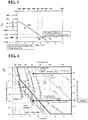
- FIG. 3 is made by extracting a dissociation curve of BaCO 3 relating to the present invention from " Dissociation curves of carbonate groups of alkaline-earth salts" on page 387 of "Science of High Temperature Superconductivity” (SHOKABO Co., Ltd., published in 2001) edited by Masashi Tachiki and Toshizo Fujita .
- a carbon compound is sufficiently decomposed in an open atmosphere before pasting.
- a step through which CO 2 is released as described above the generation of the oxide superconducting material is not inhibited during main firing thermal treatment, and a superconducting layer of the oxide superconducting material can be sufficiently formed in the joining layer 31.
- the oxygen concentration is about 100 ppm as in the related art, the crystal of the oxide superconducting material excessively grows and coarsens. Even when the pasting step and the main firing thermal treatment step are performed, the temporarily fired films are not joined to each other.
- the oxygen concentration ranges from an oxygen concentration higher than the oxygen concentration (100 ppm) generally set in the decomposition of BaCO 3 as indicated by an arrow (2) in Fig. 4 , that is, an oxygen concentration of 1% to an oxygen concentration of 100% (oxygen partial pressure 1 atm) indicated by an arrow (1) in Fig. 4.
- Figure 4 is a partly revised phase diagram of YBCO in Fig. 8 of J. Am. Ceram. Soc., 89[3] 914-920 (2006 ).
- the carbon compound in the temporarily fired film can be decomposed and the micro-crystal of the oxide superconducting material can be sufficiently formed.
- the heating temperature in the micro-crystal generation step is preferably 650°C to 800°C and more preferably 650°C to 700°C.
- the heating time is preferably about 10 to 120 minutes.
- the joining surfaces on which the micro-crystal of the oxide superconducting material has been generated are overlapped each other and fixed with a pressurizing jig or the like.
- the joining surfaces are pasted to each other by being pressed at a pressure of 1 MPa or more.
- a main firing thermal treatment step is performed as a heat-joining step of joining the joining surfaces.
- heating is performed at a temperature higher than or equal to the generation temperature of the oxide superconducting material to join the joining surfaces.
- the temperature is increased to about 800°C at a heating rate of about 100 °C/ min and then decreased to room temperature at substantially the same rate.
- the micro-crystal of the oxide superconducting material generated in the previous step coarsens and grows so as to bridge the pasted joining layers 31.
- a superconducting layer of the oxide superconducting material is formed in the joining layer 31, and the oxide superconducting films 14 and 24 are joined to each other in a superconducting manner with the joining layer 31 disposed therebetween.
- the micro-crystal generation step before the pasting step by performing the micro-crystal generation step before the pasting step, the micro-crystal of the oxide superconducting material is generated while the decomposition step of BaCO 3 through which CO 2 is released is finished. Therefore, in the subsequent main firing thermal treatment step, the superconducting layer of the oxide superconducting material is sufficiently formed in the joining layer 31 and the superconducting wire materials are joined to each other. Thus, a lengthened superconducting wire material can be produced.
- the raw material solution used for forming the joining layer 31 is preferably a solution prepared by dissolving, in an organic solvent such as an alcohol, an organic compound of a metal constituting the oxide superconducting material, such as an organometallic compound not containing fluorine, e.g., an acetylacetone metal complex.
- an organic solvent such as an alcohol
- an organic compound of a metal constituting the oxide superconducting material such as an organometallic compound not containing fluorine, e.g., an acetylacetone metal complex.
- the oxide superconducting material in the superconducting layer formed on the joining surface is preferably an oxide superconducting material in which the crystal grows at a temperature equal to or lower than the crystal growth temperature of the oxide superconducting material constituting the oxide superconducting films 14 and 24.
- a vapor deposition method or the like may be employed instead of the MOD method serving as a metal organic deposition method.
- the vapor deposition method that can be preferably employed include physical vapor deposition (PVD) methods such as a pulsed laser deposition (PLD) method and an electron-beam deposition method, and chemical vapor deposition (CVD) methods such as a metal organic chemical vapor deposition (MOCVD) method.
- PVD physical vapor deposition
- PLD pulsed laser deposition
- CVD chemical vapor deposition
- MOCVD metal organic chemical vapor deposition
- the superconducting wire material is lengthened by forming the joining layer between the superconducting layers of the superconducting wire materials.
- a short superconducting joining member in which a micro-crystal of an oxide superconducting material is generated on a joining surface may be produced.
- the superconducting joining member is pasted so as to bridge oxide superconducting thin films at end portions of two superconducting wire materials, and heat-joining is performed to lengthen the superconducting wire material.
- the micro-crystal generation step of generating a micro-crystal of an oxide superconducting material is performed as a step of disposing a micro-crystal on an oxide superconducting film, but the present invention is not limited thereto.
- a joining member containing a micro-crystal of an oxide superconducting material is produced in a different step in advance, and the joining member may be placed on the oxide superconducting film.
- a superconducting layer of an oxide superconducting material can also be stably formed on the joining surface. Consequently, the superconducting wire materials can be joined to each other in a superconducting state with zero resistance.
- the joining member containing a micro-crystal can be easily produced as follows.
- a substrate for producing a joining member is separately provided, and a solution is applied onto the substrate to form a coat-film.
- the temporary firing thermal treatment step and the temporary firing film decomposition step are performed to generate a micro-crystal, and the generated micro-crystal is peeled off from the substrate.
- Another method for producing the joining member containing a micro-crystal is a method that uses electron-beam deposition.
- a substrate for producing a joining member is separately provided, and a raw material is deposited on the substrate by electron-beam deposition at room temperature. Then, the temperature is increased to 800°C in a 1% to 100% oxygen atmosphere to generate a micro-crystal. By peeling off the generated micro-crystal from the substrate, the joining member containing a micro-crystal can be easily produced.
- the superconducting wire materials are joined to each other using only the joining layer formed of the oxide superconducting material.
- a joining auxiliary member containing any of Ag, Au, and Pt is preferably placed in the joining layer.
- such a joining auxiliary member can be easily formed by adding particles of Ag, Au, or Pt to the raw material solution in the MOD method used when the micro-crystal is generated.
- the joining member containing a micro-crystal is separately produced or when a micro-crystal is generated by a method other than the MOD method, particles of Ag, Au, or Pt are placed between the joining member and the oxide superconducting film and then the heat-joining step is performed. Consequently, a joining auxiliary member containing any of Ag, Au, and Pt can be formed at an interface between the joining layer and the oxide superconducting film.
- the heat-joining step of joining the joining surfaces is preferably performed under such conditions that the micro-crystal is temporarily melted and a part of the micro-crystal, preferably 30 mass% or less of the micro-crystal, is caused to grow through a liquid phase.
- the micro-crystal By causing the micro-crystal to grow through a liquid phase, the micro-crystal can be grown within a short time to form the joining layer.
- the heating temperature and the heating atmosphere in the heat-joining step are preferably controlled.
- the temperature is increased in an oxygen concentration of several parts per million (ppm) to melt the micro-crystal and form a liquid phase.
- the oxygen concentration is changed to about 1000 ppm and the micro-crystal is rapidly coarsened and crystallized in an oriented manner.
- the micro-crystal can be grown within a short time.
- the conditions in which the micro-crystal is melted are appropriately set in accordance with, for example, the type and composition of oxide superconducting material.
- the micro-crystal is preferably disposed so as to scatter on the oxide superconducting film in the step of disposing a micro-crystal.
- the micro-crystal when the micro-crystal is directly generated on the oxide superconducting film by the MOD method as described in the above embodiment, the micro-crystal can be caused to scatter by spraying the raw material solution in the MOD method onto the oxide superconducting film.
- a particulate joining member is preferably disposed so as to scatter on the oxide superconducting film.
- the micro-crystal is preferably disposed such that a gap having an area of 10% or more of the area of the joining surface is formed.
- the ratio of the volume of a non-c-axis-oriented superconducting material in the joining layer relative to the total volume of a c-axis-oriented superconducting material and the non-c-axis-oriented superconducting material is preferably set to 10 to 95 vol%.
- the non-c-axis-oriented superconducting material is formed in the joining layer at this ratio, spaces between non-c-axis-oriented crystal grains and c-axis-oriented crystal grains serve as oxygen diffusion paths.
- a sufficient amount of oxygen is supplied to the c-axis-oriented superconducting material, which allows formation of a large amount of c-axis-oriented superconducting material into which oxygen has been introduced.
- the critical current density of an oxide superconductor is different between the ab plane and the c-axis direction.
- the critical current density of the c-axis direction is 1/10 the critical current density of the ab plane. Therefore, the area of the c-axis-oriented superconducting material at the interface between the joining layer and the oxide superconducting film needs to be 10 or more times the cross-sectional area of the superconducting layer of the superconducting wire material.
- the joining layer has a critical current higher than or equal to that of the superconducting wire material.
- yttria-stabilized zirconia When the joining layer containing the oxide superconducting material is formed, yttria-stabilized zirconia can be incorporated into the joining layer by adding an yttria-stabilized zirconia nanopowder to the solution used when the joining layer is formed.
- the yttria-stabilized zirconia has low reactivity with superconducting materials and oxygen permeability, and thus oxygen can be appropriately introduced into the c-axis-oriented superconducting material.
- a micro-crystal of an oxide superconducting material was generated on an oxide superconducting film, and superconducting wire materials were pasted to each other. Then, the micro-crystal was grown to form a joining layer. Thus, a superconducting wire material lengthened by joining two superconducting wire materials to each other was produced. It was checked whether a superconducting layer of the oxide superconducting material was formed in the joining layer.
- a metal substrate was provided by forming an intermediate layer having a thickness of 600 nm on a clad textured metal substrate having a thickness of 150 ⁇ m and made of Ni/Cu/SUS.
- a YBCO superconducting film having a thickness of 3 ⁇ m was formed on the metal substrate to produce a superconducting wire material having a width of 4 mm and a length of 100 mm.
- the alcohol solution was applied onto a surface of the YBCO superconducting film at both end portions of each superconducting wire material so as to have a thickness of about 25 ⁇ m and dried in the air at about 150°C for about 10 minutes to form a coat-film (coating area: 120 mm 2 ).
- the superconducting film on which the coat-film was formed was placed in an atmosphere having a dew point of 15°C to 20°C and an oxygen concentration of 20% and heated to 500°C at a heating rate of 2.5 °C/min to form a temporarily fired film.
- the heating atmosphere was set to a high oxygen concentration atmosphere having an oxygen concentration of 100% (oxygen partial pressure 1 atm).
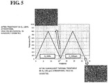
- the temperature was increased to 800°C at a heating rate of 100 °C/min for 8 minutes and then decreased to room temperature at substantially the same rate for 8 minutes (micro-crystal generation step).
- the heating atmosphere was changed to an atmosphere having an oxygen concentration of 100 ppm, and thermal treatment was performed for 16 minutes under the same heating and cooling conditions as those of the micro-crystal generation step (main firing thermal treatment step).
- the SEM image at the upper left in Fig. 5 shows that a layer having surface morphology different from that of c-axis-oriented YBCO is formed on the surface of the joining layer after the micro-crystal generation step.
- the SEM image at the lower right in Fig. 5 shows that a coarsened crystal having an average grain size of 10 ⁇ m or more is generated on the surface of the joining layer after the main firing thermal treatment step.
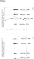
- the analysis results of 2D-XRD show in a photograph in Fig. 6(a) that, in the joining layer after the micro-crystal generation step, BaCO 3 is decomposed and a YBCO compound is formed while at the same time a ring pattern of YBa 2 Cu 3 O 7-x (103) that indicates a non-oriented micro-crystal is generated.
- the analysis results of 2D-XRD show in a photograph in Fig. 6(b) that, in the joining layer after the main firing thermal treatment step, the ring pattern is eliminated and the peak intensities of YBa 2 Cu 3 O 7-x (002, 003, 005, and 006) are increased.
- superconducting wire materials lengthened by joining two superconducting wire materials were produced by various methods including the production methods according to the above embodiments, and the performance of the produced superconducting wire materials was evaluated.
- a micro-crystal was generated on the oxide superconducting film and a joining layer was formed from the generated micro-crystal.
- two superconducting wire materials (width 4 mm and length 100 mm) were joined to each other to produce a long superconducting wire material.
- the conditions for forming the joining layer were the same as those in First Experiment, and the joining layers were pasted to each other using a jig to produce a lengthened superconducting wire material.
- a long superconducting wire material was produced by joining two superconducting wire materials under the same conditions as in Experimental Example 1, except that the heating atmosphere in the micro-crystal generation step was changed to an atmosphere having an oxygen concentration of 1%.
- a long superconducting wire material was produced by joining the same superconducting wire materials as those used in Experimental Examples 1 to 3 through diffusion joining with Ag.
- a long superconducting wire material was produced by disposing a Ag protective layer and a Cu stabilizing layer on each superconducting wire material and joining the Cu stabilizing layers with solder.
- a joining member containing a micro-crystal of a superconducting material and produced in advance was disposed between superconducting layers of two superconducting wire materials, and then the joining surfaces were heated to grow the micro-crystal. Thus, the joining surfaces were joined to each other to produce a long superconducting wire material.
- the other conditions were the same as those in Experimental Example 1.
- the resistivity (resistivity at the joining interface) and the critical current (Ic) were measured in the joining portion between the two superconducting wire materials.
- the measurement was carried out by a four-terminal method at a liquid nitrogen temperature (77 K).
- Table 1 shows the evaluation results.
- Table 1 Type of joining Resistivity at joining interface (n ⁇ ) Ic
- A Experimental Example 1 Joining by MOD method (micro-crystal generation step in an O 2 concentration of 100%) 0 200
- Experimental Example 2 Joining by MOD method (micro-crystal generation step in an O 2 concentration of 1% 0 200
- Experimental Example 3 Joining by MOD method (without micro-crystal generation step) 0 200
- Experimental Example 4 Diffusion joining with Ag 10 0
- Experimental Example 5 Joining with solder 100
- a long superconducting wire material can be produced at a high yield by stably joining a plurality of superconducting wire materials in a superconducting state.
- the present invention contributes to an improvement in production efficiency of, for example, superconducting cables and superconducting coils used in a permanent current mode.
Landscapes
- Physics & Mathematics (AREA)
- Condensed Matter Physics & Semiconductors (AREA)
- General Physics & Mathematics (AREA)
- Engineering & Computer Science (AREA)
- Manufacturing & Machinery (AREA)
- Superconductors And Manufacturing Methods Therefor (AREA)
Claims (19)
- Verfahren zur Herstellung eines supraleitenden Drahtmaterials (1), das durch Verbinden von Endabschnitten von supraleitenden Drahtmaterialien (11) verlängert wird, die jeweils einen supraleitenden Oxidfilm (14; 24) aufweisen, wobei die Endabschnitte als Verbindungsflächen dienen, wobei das Verfahren umfasst:einen Schritt des Ablagerns eines Mikrokristalls aus einem supraleitenden Oxidmaterial auf jeder der Verbindungsflächen der supraleitenden Oxidfilme,einen Klebeschritt des Überlappens und Zusammenklebens der Verbindungsflächen, auf denen der Mikrokristall angeordnet ist, undeinen Wärmeverbindungsschritt des Erwärmens der überlappenden Verbindungsflächen, um den Mikrokristall wachsen zu lassen, wodurch als eine Verbindungsschicht (31) eine supraleitende Schicht aus dem supraleitenden Oxidmaterials gebildet wird, um die Verbindungsflächen miteinander zu verbinden.
- Verfahren zur Herstellung eines supraleitenden Drahtmaterials (1) nach Anspruch 1, wobei der Schritt des Ablagerns eines Mikrokristalls ein Mikrokristallerzeugungsschritt des Erzeugens eines Mikrokristalls aus einem supraleitenden Oxidmaterial auf jeder der Verbindungsflächen der supraleitenden Oxidfilme (14; 24) ist.
- Verfahren zur Herstellung eines supraleitenden Drahtmaterials (1) nach Anspruch 2,
wobei der Schritt der Mikrokristallerzeugung umfasst:einen Beschichtungsfilmbildungsschritt des Auftragens einer Lösung, die eine organische Verbindung eines Metalls enthält, aus dem das supraleitende Oxidmaterial besteht, auf jede der Verbindungsflächen der supraleitenden Oxidfilme (14; 24), um einen Beschichtungsfilm zu bilden,einen Wärmebehandlungsschritt des temporären Brennens, bei dem der Beschichtungsfilm einer Wärmebehandlung unterzogen wird, um den Beschichtungsfilm thermisch zu zersetzen, wodurch ein Vorläufer des supraleitenden Oxidmaterials als temporär gebrannter Film gebildet wird, undeinen Schritt des Zersetzens des temporär gebrannten Films, bei dem der temporär gebrannte Film einer Wärmebehandlung in einer Atmosphäre mit einer Sauerstoffkonzentration von 1 % bis 100 % bei einer Temperatur, die größer oder gleich einer Zersetzungstemperatur des temporär gebrannten Films ist, unterzogen wird, um den temporär gebrannten Film zu zersetzen, wodurch ein Mikrokristall des supraleitenden Oxidmaterials erzeugt wird. - Verfahren zur Herstellung eines supraleitenden Drahtmaterials (1) nach Anspruch 3, wobei die organische Verbindung des Metalls eine organometallische Verbindung ist, die kein Fluor enthält.
- Verfahren zur Herstellung eines supraleitenden Drahtmaterials (1) nach Anspruch 1,
wobei der Schritt des Ablagerns eines Mikrokristalls umfasst:einen Schritt zur Herstellung eines Verbindungselements, bei dem ein Verbindungselement, das einen Mikrokristall des supraleitenden Oxidmaterials enthält, im Voraus hergestellt wird, undeinen Schritt des Platzierens des Verbindungselements, bei dem das im Voraus hergestellte Verbindungselement auf jeder der Verbindungsflächen der supraleitenden Oxidschichten platziert wird (14; 24). - Verfahren zur Herstellung eines supraleitenden Drahtmaterials (1) nach Anspruch 5,
wobei der Schritt zur Herstellung des Verbindungselements umfasst:einen Beschichtungsfilmbildungsschritt des Auftragens einer Lösung, die eine organische Verbindung eines Metalls enthält, aus dem das supraleitende Oxidmaterial besteht, auf ein Substrat für die Herstellung eines Verbindungselement, um einen Beschichtungsfilm zu bilden,einen Wärmebehandlungsschritt des temporären Brennens, bei dem der Beschichtungsfilm einer Wärmebehandlung unterzogen wird, um den Beschichtungsfilm thermisch zu zersetzen, wodurch ein Vorläufer des supraleitenden Oxidmaterials als temporär gebrannter Film gebildet wird,einen Schritt des Zersetzens des temporär gebrannten Films, bei dem der temporär gebrannte Film einer Wärmebehandlung in einer Atmosphäre mit einer Sauerstoffkonzentration von 1 % bis 100 % bei einer Temperatur, die größer oder gleich einer Zersetzungstemperatur des temporär gebrannten Films ist, unterzogen wird, um den temporär gebrannten Film zu zersetzen, wodurch ein Mikrokristall des supraleitenden Oxidmaterials erzeugt wird.einen Schälschritt des Abschälens des erzeugten Mikrokristalls von dem Substrat zur Herstellung eines Verbindungselements, um ein Verbindungselement herzustellen. - Verfahren zur Herstellung eines supraleitenden Drahtmaterials (1) nach Anspruch 6, wobei die organische Verbindung des Metalls eine organometallische Verbindung ist, die kein Fluor enthält.
- Verfahren zur Herstellung eines supraleitenden Drahtmaterials (1) nach einem der Ansprüche 1 bis 7, wobei das supraleitende Oxidmaterial, das die Verbindungsschicht (31) bildet, ein supraleitendes Oxidmaterial ist, in dem ein Kristall bei einer Temperatur wächst, die gleich oder niedriger ist als die Kristallwachstumstemperatur eines supraleitenden Oxidmaterials, das die supraleitenden Oxidfilme (14; 24) der supraleitenden Drahtmaterialien bildet.
- Verfahren zur Herstellung eines supraleitenden Drahtmaterials nach einem der Ansprüche 1 bis 8, wobei Teilchen von Ag, Au und Pt zu der Verbindungsschicht (31) hinzugefügt werden.
- Verfahren zur Herstellung eines supraleitenden Drahtmaterials (1) nach einem der Ansprüche 1 bis 9, wobei in dem Wärmeverbindungsschritt ein Teil des Mikrokristalls durch eine flüssige Phase zum Wachsen gebracht wird.
- Verfahren zur Herstellung eines supraleitenden Drahtmaterials (1) nach Anspruch 10, wobei in dem Wärmeverbindungsschritt 30 Massen-% oder weniger des Mikrokristalls durch eine flüssige Phase zum Wachsen gebracht werden.
- Verfahren zur Herstellung eines supraleitenden Drahtmaterials (1) nach einem der Ansprüche 1 bis 11, wobei in dem Schritt des Ablagerns eines Mikrokristalls der Mikrokristall so abgelagert wird, dass er an jeder der Verbindungsflächen der supraleitenden Oxidfilme (14; 24) streut.
- Verfahren zur Herstellung eines supraleitenden Drahtmaterials (1) nach Anspruch 12, wobei der Mikrokristall so abgelagert wird, dass ein Spalt mit einer Fläche von 10% oder mehr einer Fläche der Verbindungsfläche gebildet wird.
- Verfahren zur Herstellung eines supraleitenden Drahtmaterials (1) nach einem der Ansprüche 1 bis 13, wobei ein Verhältnis eines Volumens eines nicht-C-achsenorientierten supraleitenden Materials in der Verbindungsschicht (31) relativ zu einem Gesamtvolumen eines C-Achsen-orientierten supraleitenden Materials und des nicht-C-achsenorientierten supraleitenden Materials 10 bis 95 Vol% beträgt.
- Verfahren zur Herstellung eines supraleitenden Drahtmaterials (1) nach einem der Ansprüche 1 bis 14, wobei eine Fläche des C-Achsen-orientierten supraleitenden Materials an einer Grenzfläche zwischen der Verbindungsschicht (31) und dem supraleitenden Oxidfilm (14; 24) das Zehnfache oder mehr einer Querschnittsfläche der supraleitenden Schicht des supraleitenden Drahtmaterials beträgt.
- Verfahren zur Herstellung eines supraleitenden Drahtmaterials (1) nach einem der Ansprüche 1 bis 15, wobei das zur Bildung der Verbindungsschicht (31) verwendete supraleitende Oxidmaterial ein supraleitendes Oxidmaterial auf REBCO-Basis ist.
- Verfahren zur Herstellung eines supraleitenden Drahtmaterials (1) nach Anspruch 16, wobei die Verbindungsschicht (31) eine Verbindungsschicht ist, die Yttriumoxid-stabilisiertes Zirkoniumoxid enthält.
- Anordnung zur Herstellung eines verlängerten supraleitenden Drahtmaterials mit supraleitenden Oxidfilmen, die jeweils eine Verbindungsfläche aufweisen, wobei die Anordnung folgendes umfasst- einen Mikrokristall aus einem supraleitenden Oxidmaterial, der auf jeder der Verbindungsflächen der supraleitenden Oxidfilme abgelagert ist.
- Anordnung nach Anspruch 18, wobei die Anordnung umfasst:- zwei supraleitende Drahtmaterialien mit Endabschnitten, die jeweils einen supraleitenden Oxidfilm aufweisen, wobei die Endabschnitte als Verbindungsflächen dienen und wobei die Verbindungsflächen überlappt und zusammengeklebt sind, und- einen Mikrokristall aus einem supraleitenden Oxidmaterial, der auf jeder der Verbindungsflächen der supraleitenden Oxidfilme angeordnet ist.
Applications Claiming Priority (2)
| Application Number | Priority Date | Filing Date | Title |
|---|---|---|---|
| JP2015025326 | 2015-02-12 | ||
| PCT/JP2016/053182 WO2016129469A1 (ja) | 2015-02-12 | 2016-02-03 | 超電導線材の製造方法および超電導線材接合用部材 |
Publications (3)
| Publication Number | Publication Date |
|---|---|
| EP3258471A1 EP3258471A1 (de) | 2017-12-20 |
| EP3258471A4 EP3258471A4 (de) | 2018-02-21 |
| EP3258471B1 true EP3258471B1 (de) | 2020-09-30 |
Family
ID=56614747
Family Applications (1)
| Application Number | Title | Priority Date | Filing Date |
|---|---|---|---|
| EP16749113.3A Active EP3258471B1 (de) | 2015-02-12 | 2016-02-03 | Verfahren zur herstellung eines supraleitenden drahtmaterials und verbindungselement für ein supraleitendes drahtmaterial |
Country Status (6)
| Country | Link |
|---|---|
| US (1) | US10706991B2 (de) |
| EP (1) | EP3258471B1 (de) |
| JP (2) | JP6675590B2 (de) |
| KR (1) | KR102096697B1 (de) |
| CN (1) | CN107210099B (de) |
| WO (1) | WO2016129469A1 (de) |
Families Citing this family (18)
| Publication number | Priority date | Publication date | Assignee | Title |
|---|---|---|---|---|
| DE102015219956A1 (de) * | 2015-10-14 | 2017-04-20 | Bruker Hts Gmbh | Supraleiterstruktur zur Verbindung von Bandleitern, insbesondere mit einer gewellt oder gezackt verlaufenden Naht |
| JP2018142409A (ja) * | 2017-02-27 | 2018-09-13 | 古河電気工業株式会社 | 超電導線材の接続構造 |
| CN110637347B (zh) | 2017-05-15 | 2021-05-25 | 国立研究开发法人理化学研究所 | 超导磁体 |
| CN110582815B (zh) * | 2017-05-19 | 2021-01-01 | 住友电气工业株式会社 | 超导线、超导线圈、超导磁体和超导设备 |
| WO2018211766A1 (ja) * | 2017-05-19 | 2018-11-22 | 住友電気工業株式会社 | 超電導線材、超電導コイル、超電導マグネット及び超電導機器 |
| WO2018211764A1 (ja) * | 2017-05-19 | 2018-11-22 | 住友電気工業株式会社 | 超電導線材、超電導コイル、超電導マグネットおよび超電導機器 |
| JP6869868B2 (ja) * | 2017-10-12 | 2021-05-12 | 株式会社フジクラ | 酸化物超電導線材の接続構造 |
| JP6904875B2 (ja) * | 2017-10-13 | 2021-07-21 | 株式会社フジクラ | 酸化物超電導線材の接続構造および酸化物超電導線材の接続方法 |
| WO2020161909A1 (ja) * | 2019-02-08 | 2020-08-13 | 住友電気工業株式会社 | 超電導線材接続構造 |
| JP7342310B2 (ja) * | 2019-05-28 | 2023-09-12 | 国立大学法人東北大学 | 電源装置、超伝導装置、超伝導デバイス、及び超伝導デバイスの製造方法 |
| JP2021068583A (ja) * | 2019-10-23 | 2021-04-30 | 住友電気工業株式会社 | 超電導線材接続構造 |
| JP7481963B2 (ja) | 2020-09-01 | 2024-05-13 | 株式会社東芝 | 超電導層の接続構造、超電導線材、超電導コイル、超電導機器、及び超電導層の接続方法 |
| JP7581165B2 (ja) * | 2021-09-14 | 2024-11-12 | 株式会社東芝 | 超電導層の接続構造、超電導線材、超電導コイル、超電導機器、及び超電導層の接続方法 |
| DE112022005971T5 (de) | 2021-12-15 | 2024-10-02 | Sumitomo Electric Industries, Ltd. | Supraleitfähige Drahtverbindungsstruktur |
| JP7615072B2 (ja) | 2022-02-24 | 2025-01-16 | 株式会社東芝 | 超電導層の接続構造、超電導線材、超電導コイル、超電導機器 |
| JP7731859B2 (ja) * | 2022-09-20 | 2025-09-01 | 株式会社東芝 | 超電導層の接続構造、超電導線材、超電導コイル、及び超電導機器 |
| JP7652214B2 (ja) * | 2023-02-22 | 2025-03-27 | 住友電気工業株式会社 | 超電導線材の製造方法 |
| WO2024247599A1 (ja) * | 2023-05-30 | 2024-12-05 | 住友電気工業株式会社 | 超電導線材接続構造の製造方法及び超電導線材接続構造 |
Family Cites Families (13)
| Publication number | Priority date | Publication date | Assignee | Title |
|---|---|---|---|---|
| US3434021A (en) | 1967-01-13 | 1969-03-18 | Rca Corp | Insulated gate field effect transistor |
| JPH05279028A (ja) * | 1992-03-31 | 1993-10-26 | Ngk Insulators Ltd | 希土類系超電導性組成物及びその製造方法 |
| JPH1167523A (ja) * | 1997-08-21 | 1999-03-09 | Toshiba Corp | 酸化物超電導線材の接続方法、酸化物超電導コイル装置およびそれを用いた超電導装置 |
| JP2001155566A (ja) * | 1999-12-01 | 2001-06-08 | Internatl Superconductivity Technology Center | 超電導体の接合方法及び超電導体接合部材 |
| US6383989B2 (en) * | 2000-06-21 | 2002-05-07 | The Regents Of The University Of California | Architecture for high critical current superconducting tapes |
| JP4810268B2 (ja) | 2006-03-28 | 2011-11-09 | 株式会社東芝 | 超電導線材の接続方法及び超電導線材 |
| US20100210468A1 (en) | 2008-08-04 | 2010-08-19 | Haigun Lee | Method for joining second-generation high-temperature superconducting wires by melting diffusion |
| JP5400416B2 (ja) * | 2009-02-20 | 2014-01-29 | 中部電力株式会社 | 超電導線材 |
| JP5568361B2 (ja) | 2010-04-16 | 2014-08-06 | 株式会社フジクラ | 超電導線材の電極部接合構造、超電導線材、及び超電導コイル |
| JP5615616B2 (ja) * | 2010-07-27 | 2014-10-29 | 昭和電線ケーブルシステム株式会社 | テープ状酸化物超電導体及びその製造方法 |
| JP5828299B2 (ja) | 2012-05-08 | 2015-12-02 | 住友電気工業株式会社 | 高温超電導薄膜線材の接合方法および高温超電導薄膜線材 |
| JP6419732B2 (ja) * | 2014-02-04 | 2018-11-07 | 国立研究開発法人理化学研究所 | 高温超伝導線材の低抵抗接続体および接続方法 |
| JP6371395B2 (ja) * | 2014-08-12 | 2018-08-08 | 国立研究開発法人理化学研究所 | 高温超伝導多芯テープ線、その製造方法、および製造装置 |
-
2016
- 2016-02-03 US US15/547,813 patent/US10706991B2/en active Active
- 2016-02-03 KR KR1020177022386A patent/KR102096697B1/ko active Active
- 2016-02-03 EP EP16749113.3A patent/EP3258471B1/de active Active
- 2016-02-03 CN CN201680010056.2A patent/CN107210099B/zh active Active
- 2016-02-03 WO PCT/JP2016/053182 patent/WO2016129469A1/ja not_active Ceased
- 2016-02-03 JP JP2016574752A patent/JP6675590B2/ja active Active
-
2019
- 2019-11-27 JP JP2019214308A patent/JP6804050B2/ja active Active
Non-Patent Citations (1)
| Title |
|---|
| None * |
Also Published As
| Publication number | Publication date |
|---|---|
| JP6804050B2 (ja) | 2020-12-23 |
| CN107210099A (zh) | 2017-09-26 |
| EP3258471A1 (de) | 2017-12-20 |
| US20180025812A1 (en) | 2018-01-25 |
| KR20170117414A (ko) | 2017-10-23 |
| JP6675590B2 (ja) | 2020-04-01 |
| WO2016129469A1 (ja) | 2016-08-18 |
| CN107210099B (zh) | 2019-04-12 |
| JPWO2016129469A1 (ja) | 2017-11-24 |
| KR102096697B1 (ko) | 2020-04-02 |
| EP3258471A4 (de) | 2018-02-21 |
| US10706991B2 (en) | 2020-07-07 |
| JP2020057607A (ja) | 2020-04-09 |
Similar Documents
| Publication | Publication Date | Title |
|---|---|---|
| EP3258471B1 (de) | Verfahren zur herstellung eines supraleitenden drahtmaterials und verbindungselement für ein supraleitendes drahtmaterial | |
| US7816303B2 (en) | Architecture for high temperature superconductor wire | |
| CN1208850C (zh) | 增强的涂布高温超导体 | |
| CN101449341B (zh) | 超导薄膜材料及其制造方法 | |
| US11657930B2 (en) | High temperature superconducting wires having increased engineering current densities | |
| CN103548100B (zh) | 超导薄膜材料和其制造方法 | |
| KR20130008599A (ko) | 단일 코팅에 의한 산화물 후막 | |
| JP2003300726A (ja) | テープ状酸化物超電導体及びその製造方法 | |
| JP2005044636A (ja) | 超電導線材 | |
| EP2453447B1 (de) | Substrat, verfahren zur herstellung eines supraleitenden drahts eines substrats und verfahren zur herstellung eines supraleitenden drahts | |
| RU2696182C1 (ru) | Способ изготовления высокотемпературной сверхпроводящей ленты и лента | |
| RU2481673C1 (ru) | Способ изготовления тонкопленочного высокотемпературного сверхпроводящего материала | |
| JP2005001935A (ja) | 酸化物薄膜の製造方法 | |
| JP4128358B2 (ja) | 酸化物超電導導体の製造方法 | |
| JP2015032362A (ja) | 酸化物超電導線材の製造方法 | |
| JP2010123433A (ja) | Re123超電導薄膜線材の製造方法およびre123超電導薄膜線材 | |
| JP4732162B2 (ja) | 酸化物超電導導体とその製造方法 | |
| JP6587839B2 (ja) | 酸化物超電導線材の製造方法 | |
| JP2010238633A (ja) | 希土類系厚膜酸化物超電導線材の製造方法 |
Legal Events
| Date | Code | Title | Description |
|---|---|---|---|
| STAA | Information on the status of an ep patent application or granted ep patent |
Free format text: STATUS: THE INTERNATIONAL PUBLICATION HAS BEEN MADE |
|
| PUAI | Public reference made under article 153(3) epc to a published international application that has entered the european phase |
Free format text: ORIGINAL CODE: 0009012 |
|
| STAA | Information on the status of an ep patent application or granted ep patent |
Free format text: STATUS: REQUEST FOR EXAMINATION WAS MADE |
|
| 17P | Request for examination filed |
Effective date: 20170807 |
|
| AK | Designated contracting states |
Kind code of ref document: A1 Designated state(s): AL AT BE BG CH CY CZ DE DK EE ES FI FR GB GR HR HU IE IS IT LI LT LU LV MC MK MT NL NO PL PT RO RS SE SI SK SM TR |
|
| AX | Request for extension of the european patent |
Extension state: BA ME |
|
| REG | Reference to a national code |
Ref country code: DE Ref legal event code: R079 Ref document number: 602016044977 Country of ref document: DE Free format text: PREVIOUS MAIN CLASS: H01B0013000000 Ipc: H01L0039020000 |
|
| A4 | Supplementary search report drawn up and despatched |
Effective date: 20180118 |
|
| RIC1 | Information provided on ipc code assigned before grant |
Ipc: H01B 12/06 20060101ALI20180112BHEP Ipc: H01B 13/00 20060101ALI20180112BHEP Ipc: H01L 39/02 20060101AFI20180112BHEP Ipc: H01R 4/68 20060101ALI20180112BHEP |
|
| DAV | Request for validation of the european patent (deleted) | ||
| DAX | Request for extension of the european patent (deleted) | ||
| GRAP | Despatch of communication of intention to grant a patent |
Free format text: ORIGINAL CODE: EPIDOSNIGR1 |
|
| STAA | Information on the status of an ep patent application or granted ep patent |
Free format text: STATUS: GRANT OF PATENT IS INTENDED |
|
| INTG | Intention to grant announced |
Effective date: 20200415 |
|
| GRAS | Grant fee paid |
Free format text: ORIGINAL CODE: EPIDOSNIGR3 |
|
| GRAA | (expected) grant |
Free format text: ORIGINAL CODE: 0009210 |
|
| STAA | Information on the status of an ep patent application or granted ep patent |
Free format text: STATUS: THE PATENT HAS BEEN GRANTED |
|
| AK | Designated contracting states |
Kind code of ref document: B1 Designated state(s): AL AT BE BG CH CY CZ DE DK EE ES FI FR GB GR HR HU IE IS IT LI LT LU LV MC MK MT NL NO PL PT RO RS SE SI SK SM TR |
|
| REG | Reference to a national code |
Ref country code: GB Ref legal event code: FG4D Ref country code: CH Ref legal event code: EP |
|
| REG | Reference to a national code |
Ref country code: AT Ref legal event code: REF Ref document number: 1319704 Country of ref document: AT Kind code of ref document: T Effective date: 20201015 |
|
| REG | Reference to a national code |
Ref country code: DE Ref legal event code: R096 Ref document number: 602016044977 Country of ref document: DE |
|
| REG | Reference to a national code |
Ref country code: IE Ref legal event code: FG4D |
|
| PG25 | Lapsed in a contracting state [announced via postgrant information from national office to epo] |
Ref country code: SE Free format text: LAPSE BECAUSE OF FAILURE TO SUBMIT A TRANSLATION OF THE DESCRIPTION OR TO PAY THE FEE WITHIN THE PRESCRIBED TIME-LIMIT Effective date: 20200930 Ref country code: FI Free format text: LAPSE BECAUSE OF FAILURE TO SUBMIT A TRANSLATION OF THE DESCRIPTION OR TO PAY THE FEE WITHIN THE PRESCRIBED TIME-LIMIT Effective date: 20200930 Ref country code: GR Free format text: LAPSE BECAUSE OF FAILURE TO SUBMIT A TRANSLATION OF THE DESCRIPTION OR TO PAY THE FEE WITHIN THE PRESCRIBED TIME-LIMIT Effective date: 20201231 Ref country code: NO Free format text: LAPSE BECAUSE OF FAILURE TO SUBMIT A TRANSLATION OF THE DESCRIPTION OR TO PAY THE FEE WITHIN THE PRESCRIBED TIME-LIMIT Effective date: 20201230 Ref country code: BG Free format text: LAPSE BECAUSE OF FAILURE TO SUBMIT A TRANSLATION OF THE DESCRIPTION OR TO PAY THE FEE WITHIN THE PRESCRIBED TIME-LIMIT Effective date: 20201230 Ref country code: HR Free format text: LAPSE BECAUSE OF FAILURE TO SUBMIT A TRANSLATION OF THE DESCRIPTION OR TO PAY THE FEE WITHIN THE PRESCRIBED TIME-LIMIT Effective date: 20200930 |
|
| REG | Reference to a national code |
Ref country code: AT Ref legal event code: MK05 Ref document number: 1319704 Country of ref document: AT Kind code of ref document: T Effective date: 20200930 |
|
| PG25 | Lapsed in a contracting state [announced via postgrant information from national office to epo] |
Ref country code: LV Free format text: LAPSE BECAUSE OF FAILURE TO SUBMIT A TRANSLATION OF THE DESCRIPTION OR TO PAY THE FEE WITHIN THE PRESCRIBED TIME-LIMIT Effective date: 20200930 Ref country code: RS Free format text: LAPSE BECAUSE OF FAILURE TO SUBMIT A TRANSLATION OF THE DESCRIPTION OR TO PAY THE FEE WITHIN THE PRESCRIBED TIME-LIMIT Effective date: 20200930 |
|
| REG | Reference to a national code |
Ref country code: NL Ref legal event code: MP Effective date: 20200930 |
|
| REG | Reference to a national code |
Ref country code: LT Ref legal event code: MG4D |
|
| PG25 | Lapsed in a contracting state [announced via postgrant information from national office to epo] |
Ref country code: LT Free format text: LAPSE BECAUSE OF FAILURE TO SUBMIT A TRANSLATION OF THE DESCRIPTION OR TO PAY THE FEE WITHIN THE PRESCRIBED TIME-LIMIT Effective date: 20200930 Ref country code: NL Free format text: LAPSE BECAUSE OF FAILURE TO SUBMIT A TRANSLATION OF THE DESCRIPTION OR TO PAY THE FEE WITHIN THE PRESCRIBED TIME-LIMIT Effective date: 20200930 Ref country code: PT Free format text: LAPSE BECAUSE OF FAILURE TO SUBMIT A TRANSLATION OF THE DESCRIPTION OR TO PAY THE FEE WITHIN THE PRESCRIBED TIME-LIMIT Effective date: 20210201 Ref country code: RO Free format text: LAPSE BECAUSE OF FAILURE TO SUBMIT A TRANSLATION OF THE DESCRIPTION OR TO PAY THE FEE WITHIN THE PRESCRIBED TIME-LIMIT Effective date: 20200930 Ref country code: SM Free format text: LAPSE BECAUSE OF FAILURE TO SUBMIT A TRANSLATION OF THE DESCRIPTION OR TO PAY THE FEE WITHIN THE PRESCRIBED TIME-LIMIT Effective date: 20200930 Ref country code: CZ Free format text: LAPSE BECAUSE OF FAILURE TO SUBMIT A TRANSLATION OF THE DESCRIPTION OR TO PAY THE FEE WITHIN THE PRESCRIBED TIME-LIMIT Effective date: 20200930 Ref country code: EE Free format text: LAPSE BECAUSE OF FAILURE TO SUBMIT A TRANSLATION OF THE DESCRIPTION OR TO PAY THE FEE WITHIN THE PRESCRIBED TIME-LIMIT Effective date: 20200930 |
|
| PG25 | Lapsed in a contracting state [announced via postgrant information from national office to epo] |
Ref country code: ES Free format text: LAPSE BECAUSE OF FAILURE TO SUBMIT A TRANSLATION OF THE DESCRIPTION OR TO PAY THE FEE WITHIN THE PRESCRIBED TIME-LIMIT Effective date: 20200930 Ref country code: AT Free format text: LAPSE BECAUSE OF FAILURE TO SUBMIT A TRANSLATION OF THE DESCRIPTION OR TO PAY THE FEE WITHIN THE PRESCRIBED TIME-LIMIT Effective date: 20200930 Ref country code: AL Free format text: LAPSE BECAUSE OF FAILURE TO SUBMIT A TRANSLATION OF THE DESCRIPTION OR TO PAY THE FEE WITHIN THE PRESCRIBED TIME-LIMIT Effective date: 20200930 Ref country code: PL Free format text: LAPSE BECAUSE OF FAILURE TO SUBMIT A TRANSLATION OF THE DESCRIPTION OR TO PAY THE FEE WITHIN THE PRESCRIBED TIME-LIMIT Effective date: 20200930 Ref country code: IS Free format text: LAPSE BECAUSE OF FAILURE TO SUBMIT A TRANSLATION OF THE DESCRIPTION OR TO PAY THE FEE WITHIN THE PRESCRIBED TIME-LIMIT Effective date: 20210130 |
|
| PG25 | Lapsed in a contracting state [announced via postgrant information from national office to epo] |
Ref country code: SK Free format text: LAPSE BECAUSE OF FAILURE TO SUBMIT A TRANSLATION OF THE DESCRIPTION OR TO PAY THE FEE WITHIN THE PRESCRIBED TIME-LIMIT Effective date: 20200930 |
|
| REG | Reference to a national code |
Ref country code: DE Ref legal event code: R097 Ref document number: 602016044977 Country of ref document: DE |
|
| PLBE | No opposition filed within time limit |
Free format text: ORIGINAL CODE: 0009261 |
|
| STAA | Information on the status of an ep patent application or granted ep patent |
Free format text: STATUS: NO OPPOSITION FILED WITHIN TIME LIMIT |
|
| PG25 | Lapsed in a contracting state [announced via postgrant information from national office to epo] |
Ref country code: DK Free format text: LAPSE BECAUSE OF FAILURE TO SUBMIT A TRANSLATION OF THE DESCRIPTION OR TO PAY THE FEE WITHIN THE PRESCRIBED TIME-LIMIT Effective date: 20200930 |
|
| 26N | No opposition filed |
Effective date: 20210701 |
|
| PG25 | Lapsed in a contracting state [announced via postgrant information from national office to epo] |
Ref country code: MC Free format text: LAPSE BECAUSE OF FAILURE TO SUBMIT A TRANSLATION OF THE DESCRIPTION OR TO PAY THE FEE WITHIN THE PRESCRIBED TIME-LIMIT Effective date: 20200930 |
|
| GBPC | Gb: european patent ceased through non-payment of renewal fee |
Effective date: 20210203 |
|
| REG | Reference to a national code |
Ref country code: BE Ref legal event code: MM Effective date: 20210228 |
|
| PG25 | Lapsed in a contracting state [announced via postgrant information from national office to epo] |
Ref country code: IT Free format text: LAPSE BECAUSE OF FAILURE TO SUBMIT A TRANSLATION OF THE DESCRIPTION OR TO PAY THE FEE WITHIN THE PRESCRIBED TIME-LIMIT Effective date: 20200930 Ref country code: CH Free format text: LAPSE BECAUSE OF NON-PAYMENT OF DUE FEES Effective date: 20210228 Ref country code: LU Free format text: LAPSE BECAUSE OF NON-PAYMENT OF DUE FEES Effective date: 20210203 Ref country code: LI Free format text: LAPSE BECAUSE OF NON-PAYMENT OF DUE FEES Effective date: 20210228 |
|
| PG25 | Lapsed in a contracting state [announced via postgrant information from national office to epo] |
Ref country code: SI Free format text: LAPSE BECAUSE OF FAILURE TO SUBMIT A TRANSLATION OF THE DESCRIPTION OR TO PAY THE FEE WITHIN THE PRESCRIBED TIME-LIMIT Effective date: 20200930 |
|
| PG25 | Lapsed in a contracting state [announced via postgrant information from national office to epo] |
Ref country code: GB Free format text: LAPSE BECAUSE OF NON-PAYMENT OF DUE FEES Effective date: 20210203 Ref country code: IE Free format text: LAPSE BECAUSE OF NON-PAYMENT OF DUE FEES Effective date: 20210203 Ref country code: FR Free format text: LAPSE BECAUSE OF NON-PAYMENT OF DUE FEES Effective date: 20210228 |
|
| PG25 | Lapsed in a contracting state [announced via postgrant information from national office to epo] |
Ref country code: IS Free format text: LAPSE BECAUSE OF FAILURE TO SUBMIT A TRANSLATION OF THE DESCRIPTION OR TO PAY THE FEE WITHIN THE PRESCRIBED TIME-LIMIT Effective date: 20210130 |
|
| PG25 | Lapsed in a contracting state [announced via postgrant information from national office to epo] |
Ref country code: BE Free format text: LAPSE BECAUSE OF NON-PAYMENT OF DUE FEES Effective date: 20210228 |
|
| REG | Reference to a national code |
Ref country code: DE Ref legal event code: R079 Ref document number: 602016044977 Country of ref document: DE Free format text: PREVIOUS MAIN CLASS: H01L0039020000 Ipc: H10N0060800000 |
|
| REG | Reference to a national code |
Ref country code: DE Ref legal event code: R082 Ref document number: 602016044977 Country of ref document: DE Representative=s name: CBDL PATENTANWAELTE GBR, DE Ref country code: DE Ref legal event code: R082 Ref document number: 602016044977 Country of ref document: DE Representative=s name: CBDL PATENTANWAELTE EGBR, DE |
|
| P01 | Opt-out of the competence of the unified patent court (upc) registered |
Effective date: 20230515 |
|
| PG25 | Lapsed in a contracting state [announced via postgrant information from national office to epo] |
Ref country code: CY Free format text: LAPSE BECAUSE OF FAILURE TO SUBMIT A TRANSLATION OF THE DESCRIPTION OR TO PAY THE FEE WITHIN THE PRESCRIBED TIME-LIMIT Effective date: 20200930 |
|
| PG25 | Lapsed in a contracting state [announced via postgrant information from national office to epo] |
Ref country code: HU Free format text: LAPSE BECAUSE OF FAILURE TO SUBMIT A TRANSLATION OF THE DESCRIPTION OR TO PAY THE FEE WITHIN THE PRESCRIBED TIME-LIMIT; INVALID AB INITIO Effective date: 20160203 |
|
| PG25 | Lapsed in a contracting state [announced via postgrant information from national office to epo] |
Ref country code: MK Free format text: LAPSE BECAUSE OF FAILURE TO SUBMIT A TRANSLATION OF THE DESCRIPTION OR TO PAY THE FEE WITHIN THE PRESCRIBED TIME-LIMIT Effective date: 20200930 |
|
| PG25 | Lapsed in a contracting state [announced via postgrant information from national office to epo] |
Ref country code: MT Free format text: LAPSE BECAUSE OF FAILURE TO SUBMIT A TRANSLATION OF THE DESCRIPTION OR TO PAY THE FEE WITHIN THE PRESCRIBED TIME-LIMIT Effective date: 20200930 |
|
| PG25 | Lapsed in a contracting state [announced via postgrant information from national office to epo] |
Ref country code: TR Free format text: LAPSE BECAUSE OF FAILURE TO SUBMIT A TRANSLATION OF THE DESCRIPTION OR TO PAY THE FEE WITHIN THE PRESCRIBED TIME-LIMIT Effective date: 20200930 |
|
| PGFP | Annual fee paid to national office [announced via postgrant information from national office to epo] |
Ref country code: DE Payment date: 20251230 Year of fee payment: 11 |