EP3258496A1 - Anzeigevorrichtung - Google Patents
Anzeigevorrichtung Download PDFInfo
- Publication number
- EP3258496A1 EP3258496A1 EP17176364.2A EP17176364A EP3258496A1 EP 3258496 A1 EP3258496 A1 EP 3258496A1 EP 17176364 A EP17176364 A EP 17176364A EP 3258496 A1 EP3258496 A1 EP 3258496A1
- Authority
- EP
- European Patent Office
- Prior art keywords
- line
- conductive line
- display apparatus
- insulation layer
- layer
- Prior art date
- Legal status (The legal status is an assumption and is not a legal conclusion. Google has not performed a legal analysis and makes no representation as to the accuracy of the status listed.)
- Granted
Links
Images





Classifications
-
- H—ELECTRICITY
- H10—SEMICONDUCTOR DEVICES; ELECTRIC SOLID-STATE DEVICES NOT OTHERWISE PROVIDED FOR
- H10K—ORGANIC ELECTRIC SOLID-STATE DEVICES
- H10K59/00—Integrated devices, or assemblies of multiple devices, comprising at least one organic light-emitting element covered by group H10K50/00
- H10K59/10—OLED displays
- H10K59/12—Active-matrix OLED [AMOLED] displays
- H10K59/131—Interconnections, e.g. wiring lines or terminals
-
- H—ELECTRICITY
- H10—SEMICONDUCTOR DEVICES; ELECTRIC SOLID-STATE DEVICES NOT OTHERWISE PROVIDED FOR
- H10K—ORGANIC ELECTRIC SOLID-STATE DEVICES
- H10K50/00—Organic light-emitting devices
- H10K50/80—Constructional details
- H10K50/805—Electrodes
- H10K50/82—Cathodes
- H10K50/824—Cathodes combined with auxiliary electrodes
-
- H—ELECTRICITY
- H10—SEMICONDUCTOR DEVICES; ELECTRIC SOLID-STATE DEVICES NOT OTHERWISE PROVIDED FOR
- H10K—ORGANIC ELECTRIC SOLID-STATE DEVICES
- H10K59/00—Integrated devices, or assemblies of multiple devices, comprising at least one organic light-emitting element covered by group H10K50/00
- H10K59/10—OLED displays
- H10K59/12—Active-matrix OLED [AMOLED] displays
- H10K59/122—Pixel-defining structures or layers, e.g. banks
-
- H—ELECTRICITY
- H10—SEMICONDUCTOR DEVICES; ELECTRIC SOLID-STATE DEVICES NOT OTHERWISE PROVIDED FOR
- H10K—ORGANIC ELECTRIC SOLID-STATE DEVICES
- H10K59/00—Integrated devices, or assemblies of multiple devices, comprising at least one organic light-emitting element covered by group H10K50/00
- H10K59/10—OLED displays
- H10K59/12—Active-matrix OLED [AMOLED] displays
- H10K59/123—Connection of the pixel electrodes to the thin film transistors [TFT]
-
- H—ELECTRICITY
- H10—SEMICONDUCTOR DEVICES; ELECTRIC SOLID-STATE DEVICES NOT OTHERWISE PROVIDED FOR
- H10K—ORGANIC ELECTRIC SOLID-STATE DEVICES
- H10K59/00—Integrated devices, or assemblies of multiple devices, comprising at least one organic light-emitting element covered by group H10K50/00
- H10K59/10—OLED displays
- H10K59/12—Active-matrix OLED [AMOLED] displays
- H10K59/124—Insulating layers formed between TFT elements and OLED elements
-
- H—ELECTRICITY
- H10—SEMICONDUCTOR DEVICES; ELECTRIC SOLID-STATE DEVICES NOT OTHERWISE PROVIDED FOR
- H10K—ORGANIC ELECTRIC SOLID-STATE DEVICES
- H10K59/00—Integrated devices, or assemblies of multiple devices, comprising at least one organic light-emitting element covered by group H10K50/00
- H10K59/80—Constructional details
- H10K59/805—Electrodes
- H10K59/8052—Cathodes
- H10K59/80522—Cathodes combined with auxiliary electrodes
Definitions
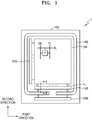
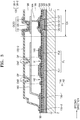
- a display apparatus is provided as follows.
- a substrate includes a display area.
- a first conductive line is positioned outside the display area of the substrate.
- a passivation layer covers a portion of the first conductive line.
- a first connection line is positioned on the passivation layer. The first connection line is in contact with the first conductive line.
- An insulation layer is positioned on the passivation layer and the first connection line. The insulation layer includes at least one opening.
- a second connection line is positioned on the insulation layer. The second connection line is in contact with the first connection line via the at least one opening and has an end portion that contacts the first conductive line.
- a second conductive line is positioned between the display area and the first conductive line.
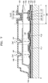
- FIGS. 8 and 9 Since the other elements illustrated in FIGS. 8 and 9 are the same as those in the above exemplary embodiments, repeated descriptions thereof will be omitted.
- the thin film transistor of the above exemplary embodiments is a top-gate type thin film transistor.
- the present invention is not limited thereto.
- the thin film transistor may be a bottom-gate type thin film transistor.
- the gate electrode may be the second interlayer insulation layer 103.
Landscapes
- Engineering & Computer Science (AREA)
- Microelectronics & Electronic Packaging (AREA)
- Physics & Mathematics (AREA)
- Optics & Photonics (AREA)
- Devices For Indicating Variable Information By Combining Individual Elements (AREA)
- Electroluminescent Light Sources (AREA)
- Liquid Crystal (AREA)
- Geometry (AREA)
Applications Claiming Priority (1)
| Application Number | Priority Date | Filing Date | Title |
|---|---|---|---|
| KR1020160075102A KR102654924B1 (ko) | 2016-06-16 | 2016-06-16 | 표시장치 |
Publications (2)
| Publication Number | Publication Date |
|---|---|
| EP3258496A1 true EP3258496A1 (de) | 2017-12-20 |
| EP3258496B1 EP3258496B1 (de) | 2019-03-13 |
Family
ID=59215481
Family Applications (1)
| Application Number | Title | Priority Date | Filing Date |
|---|---|---|---|
| EP17176364.2A Active EP3258496B1 (de) | 2016-06-16 | 2017-06-16 | Anzeigevorrichtung |
Country Status (4)
| Country | Link |
|---|---|
| US (2) | US10121986B2 (de) |
| EP (1) | EP3258496B1 (de) |
| KR (1) | KR102654924B1 (de) |
| CN (1) | CN107527935B (de) |
Cited By (3)
| Publication number | Priority date | Publication date | Assignee | Title |
|---|---|---|---|---|
| EP3565005A1 (de) * | 2018-05-04 | 2019-11-06 | Samsung Display Co., Ltd | Organische lichtemittierende anzeigevorrichtung |
| EP4057367A4 (de) * | 2019-11-08 | 2022-12-28 | BOE Technology Group Co., Ltd. | Anzeigesubstrat und anzeigevorrichtung damit |
| EP4325575A4 (de) * | 2021-04-13 | 2025-04-16 | Samsung Display Co., Ltd. | Anzeigevorrichtung |
Families Citing this family (24)
| Publication number | Priority date | Publication date | Assignee | Title |
|---|---|---|---|---|
| KR102654924B1 (ko) | 2016-06-16 | 2024-04-05 | 삼성디스플레이 주식회사 | 표시장치 |
| JP6947536B2 (ja) * | 2017-05-26 | 2021-10-13 | 株式会社ジャパンディスプレイ | 表示装置 |
| CN107195663B (zh) * | 2017-06-08 | 2020-09-01 | 深圳市华星光电半导体显示技术有限公司 | Amoled显示面板结构 |
| KR102550732B1 (ko) * | 2017-12-13 | 2023-07-03 | 삼성디스플레이 주식회사 | 표시장치 |
| KR102562901B1 (ko) * | 2018-03-26 | 2023-08-04 | 삼성디스플레이 주식회사 | 디스플레이 장치 |
| TWI674662B (zh) | 2018-06-19 | 2019-10-11 | 友達光電股份有限公司 | 陣列基板的製造方法 |
| KR102605335B1 (ko) * | 2018-06-27 | 2023-11-27 | 삼성디스플레이 주식회사 | 발광 표시 장치 및 그의 제조 방법 |
| CN109742087B (zh) * | 2018-12-27 | 2021-08-24 | 武汉华星光电技术有限公司 | 阵列基板及其制备方法 |
| KR102793997B1 (ko) * | 2019-02-12 | 2025-04-14 | 삼성디스플레이 주식회사 | 표시 장치 및 이의 제조 방법 |
| KR102792806B1 (ko) * | 2019-04-01 | 2025-04-14 | 삼성디스플레이 주식회사 | 표시 장치 |
| KR102707561B1 (ko) * | 2019-04-02 | 2024-09-20 | 삼성디스플레이 주식회사 | 표시 장치 |
| CN110189639B (zh) * | 2019-06-28 | 2020-12-04 | 昆山国显光电有限公司 | 显示基板、显示面板及显示装置 |
| KR102895954B1 (ko) | 2019-10-17 | 2025-12-04 | 삼성디스플레이 주식회사 | 표시장치 |
| KR102721063B1 (ko) * | 2020-02-11 | 2024-10-25 | 삼성디스플레이 주식회사 | 표시 장치 |
| KR102888566B1 (ko) | 2020-02-21 | 2025-11-21 | 삼성디스플레이 주식회사 | 표시 장치 |
| KR102791851B1 (ko) * | 2020-02-27 | 2025-04-09 | 삼성디스플레이 주식회사 | 표시 장치 및 그의 제조 방법 |
| CN111326563B (zh) * | 2020-03-05 | 2022-08-05 | 武汉华星光电半导体显示技术有限公司 | 一种显示面板 |
| CN112530301B (zh) * | 2020-12-02 | 2023-04-21 | 湖北长江新型显示产业创新中心有限公司 | 显示面板和显示装置 |
| CN112750884B (zh) * | 2020-12-30 | 2022-06-17 | 湖北长江新型显示产业创新中心有限公司 | 一种显示面板及显示装置 |
| US12402500B2 (en) * | 2021-03-23 | 2025-08-26 | Samsung Display Co., Ltd. | Display device with dual-layer voltage transmitting lines |
| EP4203053A4 (de) | 2021-04-30 | 2023-10-25 | BOE Technology Group Co., Ltd. | Anzeigesubstrat und herstellungsverfahren dafür sowie anzeigevorrichtung |
| CN114497151B (zh) * | 2022-01-12 | 2024-07-19 | 武汉华星光电半导体显示技术有限公司 | 一种显示面板 |
| KR20230174803A (ko) | 2022-06-21 | 2023-12-29 | 삼성디스플레이 주식회사 | 표시 장치 |
| CN117558730A (zh) * | 2022-08-04 | 2024-02-13 | 群创光电股份有限公司 | 电子装置 |
Citations (3)
| Publication number | Priority date | Publication date | Assignee | Title |
|---|---|---|---|---|
| US20060060850A1 (en) * | 2004-05-29 | 2006-03-23 | Won-Kyu Kwak | Electroluminescence display device and method of manufacturing the same |
| US20110254757A1 (en) * | 2010-04-16 | 2011-10-20 | Changnam Kim | Organic light emitting diode display |
| US20140159002A1 (en) * | 2012-12-07 | 2014-06-12 | Lg Display Co., Ltd. | Organic light emitting diode device and method for fabricating the same |
Family Cites Families (29)
| Publication number | Priority date | Publication date | Assignee | Title |
|---|---|---|---|---|
| US20040224241A1 (en) * | 2003-02-03 | 2004-11-11 | Samsung Electronics Co., Ltd. | Thin film transistor array panel, manufacturing method thereof, and mask therefor |
| KR100712111B1 (ko) * | 2004-12-14 | 2007-04-27 | 삼성에스디아이 주식회사 | 보조 전극 라인을 구비하는 유기전계발광소자 및 그의제조 방법 |
| KR100784544B1 (ko) | 2006-04-12 | 2007-12-11 | 엘지전자 주식회사 | 전계 발광 표시 장치 및 그 제조방법 |
| JP2007156388A (ja) * | 2005-11-14 | 2007-06-21 | Seiko Epson Corp | 発光装置および電子機器 |
| JP4736757B2 (ja) * | 2005-12-01 | 2011-07-27 | セイコーエプソン株式会社 | 発光装置および電子機器 |
| US7679284B2 (en) * | 2007-02-08 | 2010-03-16 | Seiko Epson Corporation | Light emitting device and electronic apparatus |
| KR100830331B1 (ko) * | 2007-07-23 | 2008-05-16 | 삼성에스디아이 주식회사 | 유기발광 표시 장치 및 그의 제조 방법 |
| KR100875103B1 (ko) | 2007-11-16 | 2008-12-19 | 삼성모바일디스플레이주식회사 | 유기 발광 디스플레이 장치 |
| KR101574210B1 (ko) * | 2008-09-25 | 2015-12-07 | 삼성디스플레이 주식회사 | 유기전계발광소자 및 이의 제조방법 |
| KR101290709B1 (ko) * | 2009-12-28 | 2013-07-29 | 엘지디스플레이 주식회사 | 터치센서 인셀 타입 액정표시장치용 어레이 기판 및 이의 제조방법 |
| KR101155898B1 (ko) | 2010-05-12 | 2012-06-20 | 삼성모바일디스플레이주식회사 | 유기발광 표시장치 및 그 구동 방법 |
| KR101182233B1 (ko) | 2010-06-11 | 2012-09-12 | 삼성디스플레이 주식회사 | 유기 발광 표시 장치 |
| KR101818451B1 (ko) * | 2010-12-24 | 2018-01-16 | 엘지디스플레이 주식회사 | 유기발광다이오드 표시소자 및 그 제조방법 |
| KR101519916B1 (ko) * | 2011-04-07 | 2015-05-13 | 엘지디스플레이 주식회사 | 유기 전계 발광 표시 장치 및 그의 제조 방법 |
| KR101415684B1 (ko) * | 2011-07-07 | 2014-08-07 | 엘지디스플레이 주식회사 | 유기전계 발광소자용 기판 및 그 제조 방법 |
| CN103155019B (zh) * | 2011-09-30 | 2016-01-20 | 株式会社日本有机雷特显示器 | 薄膜晶体管阵列装置、el显示面板、el显示装置、薄膜晶体管阵列装置的制造方法以及el显示面板的制造方法 |
| CN103907218B (zh) * | 2011-11-07 | 2016-05-04 | 株式会社日本有机雷特显示器 | 有机el显示面板和有机el显示装置 |
| US9443878B2 (en) * | 2012-06-25 | 2016-09-13 | Joled Inc. | Display device and method of manufacturing display device |
| JP6056072B2 (ja) * | 2012-06-27 | 2017-01-11 | 株式会社Joled | 表示装置 |
| KR102100880B1 (ko) * | 2013-06-26 | 2020-04-14 | 엘지디스플레이 주식회사 | 유기발광 다이오드 표시장치 |
| KR20150006125A (ko) | 2013-07-08 | 2015-01-16 | 삼성디스플레이 주식회사 | 유기 발광 표시장치 및 유기 발광 표시장치의 제조 방법 |
| KR102151752B1 (ko) * | 2013-08-05 | 2020-09-04 | 삼성디스플레이 주식회사 | 유기발광 디스플레이 장치 및 그 제조방법 |
| KR102282996B1 (ko) * | 2013-10-30 | 2021-07-29 | 삼성디스플레이 주식회사 | 유기 발광 표시 장치 및 그의 제조 방법 |
| CN103926769B (zh) * | 2013-12-26 | 2016-08-24 | 上海天马微电子有限公司 | 一种阵列基板、显示面板及显示器 |
| KR102141557B1 (ko) * | 2013-12-26 | 2020-08-05 | 엘지디스플레이 주식회사 | 어레이 기판 |
| KR102279921B1 (ko) * | 2014-02-12 | 2021-07-22 | 삼성디스플레이 주식회사 | 유기 발광 표시 장치 및 이의 제조 방법 |
| KR102230006B1 (ko) * | 2014-03-18 | 2021-03-19 | 삼성디스플레이 주식회사 | 유기 발광 표시 장치 |
| KR102284754B1 (ko) * | 2014-10-27 | 2021-08-03 | 삼성디스플레이 주식회사 | 박막 트랜지스터 어레이 기판, 및 이를 포함하는 유기 발광 표시 장치 |
| KR102654924B1 (ko) | 2016-06-16 | 2024-04-05 | 삼성디스플레이 주식회사 | 표시장치 |
-
2016
- 2016-06-16 KR KR1020160075102A patent/KR102654924B1/ko active Active
- 2016-12-16 US US15/381,988 patent/US10121986B2/en active Active
-
2017
- 2017-06-15 CN CN201710451214.4A patent/CN107527935B/zh active Active
- 2017-06-16 EP EP17176364.2A patent/EP3258496B1/de active Active
-
2018
- 2018-10-04 US US16/151,832 patent/US10381592B2/en active Active
Patent Citations (3)
| Publication number | Priority date | Publication date | Assignee | Title |
|---|---|---|---|---|
| US20060060850A1 (en) * | 2004-05-29 | 2006-03-23 | Won-Kyu Kwak | Electroluminescence display device and method of manufacturing the same |
| US20110254757A1 (en) * | 2010-04-16 | 2011-10-20 | Changnam Kim | Organic light emitting diode display |
| US20140159002A1 (en) * | 2012-12-07 | 2014-06-12 | Lg Display Co., Ltd. | Organic light emitting diode device and method for fabricating the same |
Cited By (8)
| Publication number | Priority date | Publication date | Assignee | Title |
|---|---|---|---|---|
| EP3565005A1 (de) * | 2018-05-04 | 2019-11-06 | Samsung Display Co., Ltd | Organische lichtemittierende anzeigevorrichtung |
| CN110444563A (zh) * | 2018-05-04 | 2019-11-12 | 三星显示有限公司 | 有机发光显示装置 |
| US12295219B2 (en) | 2018-05-04 | 2025-05-06 | Samsung Display Co., Ltd. | Organic light-emitting display device |
| US12628517B2 (en) | 2018-05-04 | 2026-05-12 | Samsung Display Co., Ltd. | Organic light-emitting display device |
| EP4057367A4 (de) * | 2019-11-08 | 2022-12-28 | BOE Technology Group Co., Ltd. | Anzeigesubstrat und anzeigevorrichtung damit |
| US12310190B2 (en) | 2019-11-08 | 2025-05-20 | Chengdu Boe Optoelectronics Technology Co., Ltd. | Display substrate and display device |
| EP4325575A4 (de) * | 2021-04-13 | 2025-04-16 | Samsung Display Co., Ltd. | Anzeigevorrichtung |
| US12349563B2 (en) | 2021-04-13 | 2025-07-01 | Samsung Display Co., Ltd. | Display device with minimized non-display portion in bezel area |
Also Published As
| Publication number | Publication date |
|---|---|
| EP3258496B1 (de) | 2019-03-13 |
| CN107527935A (zh) | 2017-12-29 |
| KR102654924B1 (ko) | 2024-04-05 |
| US10121986B2 (en) | 2018-11-06 |
| US20170365808A1 (en) | 2017-12-21 |
| KR20170142233A (ko) | 2017-12-28 |
| CN107527935B (zh) | 2023-05-16 |
| US10381592B2 (en) | 2019-08-13 |
| US20190036065A1 (en) | 2019-01-31 |
Similar Documents
| Publication | Publication Date | Title |
|---|---|---|
| US10381592B2 (en) | Display apparatus including overlapping conductive lines | |
| US12040425B2 (en) | Self-aligned display appartus | |
| US10937838B2 (en) | Organic light emitting display device | |
| KR102541442B1 (ko) | 표시 장치 | |
| US9887252B2 (en) | Transparent display apparatus | |
| KR102516054B1 (ko) | 유기발광표시장치 및 유기발광표시장치의 제조 방법 | |
| US11201199B2 (en) | Chip on film package including a protection layer and display device including the chip on film package | |
| CN108933162B (zh) | 有机发光显示设备以及制造有机发光显示设备的方法 | |
| US11004926B2 (en) | Organic light emitting diode display device | |
| KR102047007B1 (ko) | 유기발광표시장치 및 이의 제조 방법 | |
| CN112447807B (zh) | 显示设备及制造显示设备的方法 | |
| KR20140104263A (ko) | 유기 발광 표시 장치 및 그 제조 방법 | |
| KR102512724B1 (ko) | 표시장치 및 이의 제조방법 | |
| KR20170007649A (ko) | 표시 장치 | |
| CN110299395B (zh) | 基板、包括该基板的显示装置以及该显示装置的制造方法 | |
| KR20210130608A (ko) | 발광 표시 장치 및 그 제조 방법 | |
| KR102967454B1 (ko) | 발광 표시 장치 및 그 제조 방법 |
Legal Events
| Date | Code | Title | Description |
|---|---|---|---|
| PUAI | Public reference made under article 153(3) epc to a published international application that has entered the european phase |
Free format text: ORIGINAL CODE: 0009012 |
|
| STAA | Information on the status of an ep patent application or granted ep patent |
Free format text: STATUS: THE APPLICATION HAS BEEN PUBLISHED |
|
| AK | Designated contracting states |
Kind code of ref document: A1 Designated state(s): AL AT BE BG CH CY CZ DE DK EE ES FI FR GB GR HR HU IE IS IT LI LT LU LV MC MK MT NL NO PL PT RO RS SE SI SK SM TR |
|
| AX | Request for extension of the european patent |
Extension state: BA ME |
|
| STAA | Information on the status of an ep patent application or granted ep patent |
Free format text: STATUS: REQUEST FOR EXAMINATION WAS MADE |
|
| 17P | Request for examination filed |
Effective date: 20180620 |
|
| RBV | Designated contracting states (corrected) |
Designated state(s): AL AT BE BG CH CY CZ DE DK EE ES FI FR GB GR HR HU IE IS IT LI LT LU LV MC MK MT NL NO PL PT RO RS SE SI SK SM TR |
|
| GRAP | Despatch of communication of intention to grant a patent |
Free format text: ORIGINAL CODE: EPIDOSNIGR1 |
|
| STAA | Information on the status of an ep patent application or granted ep patent |
Free format text: STATUS: GRANT OF PATENT IS INTENDED |
|
| INTG | Intention to grant announced |
Effective date: 20180925 |
|
| GRAS | Grant fee paid |
Free format text: ORIGINAL CODE: EPIDOSNIGR3 |
|
| GRAA | (expected) grant |
Free format text: ORIGINAL CODE: 0009210 |
|
| STAA | Information on the status of an ep patent application or granted ep patent |
Free format text: STATUS: THE PATENT HAS BEEN GRANTED |
|
| AK | Designated contracting states |
Kind code of ref document: B1 Designated state(s): AL AT BE BG CH CY CZ DE DK EE ES FI FR GB GR HR HU IE IS IT LI LT LU LV MC MK MT NL NO PL PT RO RS SE SI SK SM TR |
|
| REG | Reference to a national code |
Ref country code: GB Ref legal event code: FG4D |
|
| REG | Reference to a national code |
Ref country code: CH Ref legal event code: EP Ref country code: AT Ref legal event code: REF Ref document number: 1108880 Country of ref document: AT Kind code of ref document: T Effective date: 20190315 |
|
| REG | Reference to a national code |
Ref country code: IE Ref legal event code: FG4D |
|
| REG | Reference to a national code |
Ref country code: DE Ref legal event code: R096 Ref document number: 602017002657 Country of ref document: DE |
|
| REG | Reference to a national code |
Ref country code: NL Ref legal event code: MP Effective date: 20190313 |
|
| REG | Reference to a national code |
Ref country code: LT Ref legal event code: MG4D |
|
| PG25 | Lapsed in a contracting state [announced via postgrant information from national office to epo] |
Ref country code: NO Free format text: LAPSE BECAUSE OF FAILURE TO SUBMIT A TRANSLATION OF THE DESCRIPTION OR TO PAY THE FEE WITHIN THE PRESCRIBED TIME-LIMIT Effective date: 20190613 Ref country code: LT Free format text: LAPSE BECAUSE OF FAILURE TO SUBMIT A TRANSLATION OF THE DESCRIPTION OR TO PAY THE FEE WITHIN THE PRESCRIBED TIME-LIMIT Effective date: 20190313 Ref country code: SE Free format text: LAPSE BECAUSE OF FAILURE TO SUBMIT A TRANSLATION OF THE DESCRIPTION OR TO PAY THE FEE WITHIN THE PRESCRIBED TIME-LIMIT Effective date: 20190313 Ref country code: FI Free format text: LAPSE BECAUSE OF FAILURE TO SUBMIT A TRANSLATION OF THE DESCRIPTION OR TO PAY THE FEE WITHIN THE PRESCRIBED TIME-LIMIT Effective date: 20190313 |
|
| PG25 | Lapsed in a contracting state [announced via postgrant information from national office to epo] |
Ref country code: LV Free format text: LAPSE BECAUSE OF FAILURE TO SUBMIT A TRANSLATION OF THE DESCRIPTION OR TO PAY THE FEE WITHIN THE PRESCRIBED TIME-LIMIT Effective date: 20190313 Ref country code: NL Free format text: LAPSE BECAUSE OF FAILURE TO SUBMIT A TRANSLATION OF THE DESCRIPTION OR TO PAY THE FEE WITHIN THE PRESCRIBED TIME-LIMIT Effective date: 20190313 Ref country code: HR Free format text: LAPSE BECAUSE OF FAILURE TO SUBMIT A TRANSLATION OF THE DESCRIPTION OR TO PAY THE FEE WITHIN THE PRESCRIBED TIME-LIMIT Effective date: 20190313 Ref country code: BG Free format text: LAPSE BECAUSE OF FAILURE TO SUBMIT A TRANSLATION OF THE DESCRIPTION OR TO PAY THE FEE WITHIN THE PRESCRIBED TIME-LIMIT Effective date: 20190613 Ref country code: RS Free format text: LAPSE BECAUSE OF FAILURE TO SUBMIT A TRANSLATION OF THE DESCRIPTION OR TO PAY THE FEE WITHIN THE PRESCRIBED TIME-LIMIT Effective date: 20190313 Ref country code: GR Free format text: LAPSE BECAUSE OF FAILURE TO SUBMIT A TRANSLATION OF THE DESCRIPTION OR TO PAY THE FEE WITHIN THE PRESCRIBED TIME-LIMIT Effective date: 20190614 |
|
| REG | Reference to a national code |
Ref country code: AT Ref legal event code: MK05 Ref document number: 1108880 Country of ref document: AT Kind code of ref document: T Effective date: 20190313 |
|
| PG25 | Lapsed in a contracting state [announced via postgrant information from national office to epo] |
Ref country code: PT Free format text: LAPSE BECAUSE OF FAILURE TO SUBMIT A TRANSLATION OF THE DESCRIPTION OR TO PAY THE FEE WITHIN THE PRESCRIBED TIME-LIMIT Effective date: 20190713 Ref country code: SK Free format text: LAPSE BECAUSE OF FAILURE TO SUBMIT A TRANSLATION OF THE DESCRIPTION OR TO PAY THE FEE WITHIN THE PRESCRIBED TIME-LIMIT Effective date: 20190313 Ref country code: AL Free format text: LAPSE BECAUSE OF FAILURE TO SUBMIT A TRANSLATION OF THE DESCRIPTION OR TO PAY THE FEE WITHIN THE PRESCRIBED TIME-LIMIT Effective date: 20190313 Ref country code: CZ Free format text: LAPSE BECAUSE OF FAILURE TO SUBMIT A TRANSLATION OF THE DESCRIPTION OR TO PAY THE FEE WITHIN THE PRESCRIBED TIME-LIMIT Effective date: 20190313 Ref country code: IT Free format text: LAPSE BECAUSE OF FAILURE TO SUBMIT A TRANSLATION OF THE DESCRIPTION OR TO PAY THE FEE WITHIN THE PRESCRIBED TIME-LIMIT Effective date: 20190313 Ref country code: ES Free format text: LAPSE BECAUSE OF FAILURE TO SUBMIT A TRANSLATION OF THE DESCRIPTION OR TO PAY THE FEE WITHIN THE PRESCRIBED TIME-LIMIT Effective date: 20190313 Ref country code: RO Free format text: LAPSE BECAUSE OF FAILURE TO SUBMIT A TRANSLATION OF THE DESCRIPTION OR TO PAY THE FEE WITHIN THE PRESCRIBED TIME-LIMIT Effective date: 20190313 Ref country code: EE Free format text: LAPSE BECAUSE OF FAILURE TO SUBMIT A TRANSLATION OF THE DESCRIPTION OR TO PAY THE FEE WITHIN THE PRESCRIBED TIME-LIMIT Effective date: 20190313 |
|
| PG25 | Lapsed in a contracting state [announced via postgrant information from national office to epo] |
Ref country code: SM Free format text: LAPSE BECAUSE OF FAILURE TO SUBMIT A TRANSLATION OF THE DESCRIPTION OR TO PAY THE FEE WITHIN THE PRESCRIBED TIME-LIMIT Effective date: 20190313 Ref country code: PL Free format text: LAPSE BECAUSE OF FAILURE TO SUBMIT A TRANSLATION OF THE DESCRIPTION OR TO PAY THE FEE WITHIN THE PRESCRIBED TIME-LIMIT Effective date: 20190313 |
|
| REG | Reference to a national code |
Ref country code: DE Ref legal event code: R097 Ref document number: 602017002657 Country of ref document: DE |
|
| PG25 | Lapsed in a contracting state [announced via postgrant information from national office to epo] |
Ref country code: IS Free format text: LAPSE BECAUSE OF FAILURE TO SUBMIT A TRANSLATION OF THE DESCRIPTION OR TO PAY THE FEE WITHIN THE PRESCRIBED TIME-LIMIT Effective date: 20190713 Ref country code: AT Free format text: LAPSE BECAUSE OF FAILURE TO SUBMIT A TRANSLATION OF THE DESCRIPTION OR TO PAY THE FEE WITHIN THE PRESCRIBED TIME-LIMIT Effective date: 20190313 |
|
| PLBE | No opposition filed within time limit |
Free format text: ORIGINAL CODE: 0009261 |
|
| STAA | Information on the status of an ep patent application or granted ep patent |
Free format text: STATUS: NO OPPOSITION FILED WITHIN TIME LIMIT |
|
| PG25 | Lapsed in a contracting state [announced via postgrant information from national office to epo] |
Ref country code: MC Free format text: LAPSE BECAUSE OF FAILURE TO SUBMIT A TRANSLATION OF THE DESCRIPTION OR TO PAY THE FEE WITHIN THE PRESCRIBED TIME-LIMIT Effective date: 20190313 Ref country code: DK Free format text: LAPSE BECAUSE OF FAILURE TO SUBMIT A TRANSLATION OF THE DESCRIPTION OR TO PAY THE FEE WITHIN THE PRESCRIBED TIME-LIMIT Effective date: 20190313 |
|
| 26N | No opposition filed |
Effective date: 20191216 |
|
| PG25 | Lapsed in a contracting state [announced via postgrant information from national office to epo] |
Ref country code: SI Free format text: LAPSE BECAUSE OF FAILURE TO SUBMIT A TRANSLATION OF THE DESCRIPTION OR TO PAY THE FEE WITHIN THE PRESCRIBED TIME-LIMIT Effective date: 20190313 |
|
| REG | Reference to a national code |
Ref country code: BE Ref legal event code: MM Effective date: 20190630 |
|
| PG25 | Lapsed in a contracting state [announced via postgrant information from national office to epo] |
Ref country code: TR Free format text: LAPSE BECAUSE OF FAILURE TO SUBMIT A TRANSLATION OF THE DESCRIPTION OR TO PAY THE FEE WITHIN THE PRESCRIBED TIME-LIMIT Effective date: 20190313 |
|
| PG25 | Lapsed in a contracting state [announced via postgrant information from national office to epo] |
Ref country code: IE Free format text: LAPSE BECAUSE OF NON-PAYMENT OF DUE FEES Effective date: 20190616 |
|
| PG25 | Lapsed in a contracting state [announced via postgrant information from national office to epo] |
Ref country code: BE Free format text: LAPSE BECAUSE OF NON-PAYMENT OF DUE FEES Effective date: 20190630 Ref country code: LU Free format text: LAPSE BECAUSE OF NON-PAYMENT OF DUE FEES Effective date: 20190616 |
|
| REG | Reference to a national code |
Ref country code: CH Ref legal event code: PL |
|
| PG25 | Lapsed in a contracting state [announced via postgrant information from national office to epo] |
Ref country code: CH Free format text: LAPSE BECAUSE OF NON-PAYMENT OF DUE FEES Effective date: 20200630 Ref country code: LI Free format text: LAPSE BECAUSE OF NON-PAYMENT OF DUE FEES Effective date: 20200630 |
|
| PG25 | Lapsed in a contracting state [announced via postgrant information from national office to epo] |
Ref country code: CY Free format text: LAPSE BECAUSE OF FAILURE TO SUBMIT A TRANSLATION OF THE DESCRIPTION OR TO PAY THE FEE WITHIN THE PRESCRIBED TIME-LIMIT Effective date: 20190313 |
|
| PG25 | Lapsed in a contracting state [announced via postgrant information from national office to epo] |
Ref country code: MT Free format text: LAPSE BECAUSE OF FAILURE TO SUBMIT A TRANSLATION OF THE DESCRIPTION OR TO PAY THE FEE WITHIN THE PRESCRIBED TIME-LIMIT Effective date: 20190313 Ref country code: HU Free format text: LAPSE BECAUSE OF FAILURE TO SUBMIT A TRANSLATION OF THE DESCRIPTION OR TO PAY THE FEE WITHIN THE PRESCRIBED TIME-LIMIT; INVALID AB INITIO Effective date: 20170616 |
|
| PG25 | Lapsed in a contracting state [announced via postgrant information from national office to epo] |
Ref country code: MK Free format text: LAPSE BECAUSE OF FAILURE TO SUBMIT A TRANSLATION OF THE DESCRIPTION OR TO PAY THE FEE WITHIN THE PRESCRIBED TIME-LIMIT Effective date: 20190313 |
|
| REG | Reference to a national code |
Ref country code: DE Ref legal event code: R079 Ref document number: 602017002657 Country of ref document: DE Free format text: PREVIOUS MAIN CLASS: H01L0027320000 Ipc: H10K0059000000 |
|
| P01 | Opt-out of the competence of the unified patent court (upc) registered |
Effective date: 20230516 |
|
| PGFP | Annual fee paid to national office [announced via postgrant information from national office to epo] |
Ref country code: GB Payment date: 20260526 Year of fee payment: 10 |
|
| PGFP | Annual fee paid to national office [announced via postgrant information from national office to epo] |
Ref country code: DE Payment date: 20260520 Year of fee payment: 10 |
|
| PGFP | Annual fee paid to national office [announced via postgrant information from national office to epo] |
Ref country code: FR Payment date: 20260527 Year of fee payment: 10 |