EP3264155B1 - Piezoelektrisches aktuator, lichtablenker und bildprojektionsvorrichtung - Google Patents
Piezoelektrisches aktuator, lichtablenker und bildprojektionsvorrichtung Download PDFInfo
- Publication number
- EP3264155B1 EP3264155B1 EP17178097.6A EP17178097A EP3264155B1 EP 3264155 B1 EP3264155 B1 EP 3264155B1 EP 17178097 A EP17178097 A EP 17178097A EP 3264155 B1 EP3264155 B1 EP 3264155B1
- Authority
- EP
- European Patent Office
- Prior art keywords
- piezoelectric
- drive
- light
- electrode
- movable
- Prior art date
- Legal status (The legal status is an assumption and is not a legal conclusion. Google has not performed a legal analysis and makes no representation as to the accuracy of the status listed.)
- Active
Links
Images









Classifications
-
- G—PHYSICS
- G02—OPTICS
- G02B—OPTICAL ELEMENTS, SYSTEMS OR APPARATUS
- G02B26/00—Optical devices or arrangements for the control of light using movable or deformable optical elements
- G02B26/08—Optical devices or arrangements for the control of light using movable or deformable optical elements for controlling the direction of light
- G02B26/10—Scanning systems
- G02B26/101—Scanning systems with both horizontal and vertical deflecting means, e.g. raster or XY scanners
-
- G—PHYSICS
- G02—OPTICS
- G02B—OPTICAL ELEMENTS, SYSTEMS OR APPARATUS
- G02B26/00—Optical devices or arrangements for the control of light using movable or deformable optical elements
- G02B26/08—Optical devices or arrangements for the control of light using movable or deformable optical elements for controlling the direction of light
- G02B26/0816—Optical devices or arrangements for the control of light using movable or deformable optical elements for controlling the direction of light by means of one or more reflecting elements
- G02B26/0833—Optical devices or arrangements for the control of light using movable or deformable optical elements for controlling the direction of light by means of one or more reflecting elements the reflecting element being a micromechanical device, e.g. a MEMS mirror, DMD
- G02B26/0858—Optical devices or arrangements for the control of light using movable or deformable optical elements for controlling the direction of light by means of one or more reflecting elements the reflecting element being a micromechanical device, e.g. a MEMS mirror, DMD the reflecting means being moved or deformed by piezoelectric means
-
- G—PHYSICS
- G02—OPTICS
- G02B—OPTICAL ELEMENTS, SYSTEMS OR APPARATUS
- G02B26/00—Optical devices or arrangements for the control of light using movable or deformable optical elements
- G02B26/08—Optical devices or arrangements for the control of light using movable or deformable optical elements for controlling the direction of light
- G02B26/10—Scanning systems
- G02B26/105—Scanning systems with one or more pivoting mirrors or galvano-mirrors
Definitions
- a piezoelectric actuator type in which piezoelectric materials that are thinned to beam-shaped elastic members for mirror driving are superimposed is known.
- the expansion and contraction of the piezoelectric materials caused due to a piezoelectric effect are transmitted to a support body serving as a beam and the beam vibrates vertically, which causes the reflecting surface to be rotated.
- the vibrating beam for implementing non-resonant driving generally includes a plurality of return parts and a plurality of coupling parts, and has a meander shape which is substantially formed of a plurality of continuous return shapes.
- US 2015/0062683 A1 discloses an optical deflection device which includes a mirror having a reflection face for deflecting light that enters the reflection face; and a support member to support the mirror including a torsion bar having one end being continuously connected to the mirror; a beam being continuously connected to another end of the torsion bar; and a plurality of piezoelectric elements disposed on the beam including a first piezoelectric element and a second piezoelectric element.
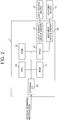
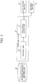
- FPGA 23 is a circuit for outputting a control signal suitable for the light source device driver 25 and the movable device driver 26 in accordance with processing of the CPU 20.
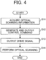
- the optical scanning information is information indicating how to perform optical scanning on the scanned surface 15.
- the optical scanning information is image data.
- the optical scanning information is write data indicating a write order or a write section.
- the optical scanning information is irradiation data indicating an irradiation range and a timing when irradiation is performed with light for object recognition.
- step S13 the drive signal output unit 31 outputs a drive signal to the light source device 12 and the movable device 13 based on the input control signal.
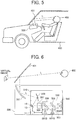
- the image projection device is a device that projects an image by optical scanning, and is, for example, a head-up display device.
- laser light from the light source device 12 such as a laser element passes through an imaging optical system 601 such as a collimator lens, and is then deflected in one axis direction or two axis directions by the movable device 13 including the reflecting surface 14.
- the laser light deflected by the movable device 13 passes through a scanning optical system 602, which is formed of a first lens 602a, a second lens 602b, and a reflective mirror unit 602c, and is emitted on the scanned surface 15 (for example, a photosensitive drum or photosensitive paper) to write light thereon.
- the scanning optical system 602 focuses light beams on the scanned surface 15 in a spot manner.
- the light source device 12 and the movable device 13 including the reflecting surface 14 are driven based on the control of the control device 11.
- the light writing device 600 described above can be used as a structural member of the image forming device including a printer function using laser light.
- the scanning optical system is varied to enable optical scanning not only in one axis direction, but also in two axis directions, and laser light is deflected on a thermal medium to be heated, so that the scanning optical system can be used as a structural member of the image forming device such as a laser label device for printing.
- the movable device 13 has a structure in which, for example, the reflecting surface 14, first piezoelectric actuation parts 112a and 112b, second piezoelectric actuation parts 131a to 131f and 132a to 132f, the electrode coupling part 160, and the like are formed on a substrate on which a single Silicon On Insulator (SOI) substrate is formed by an etching process or the like, to integrally form the components.
- SOI Silicon On Insulator
- the SOI substrate is a substrate having a structure in which a silicon oxide layer 172 is formed on a first silicon layer, which is formed of single-crystal silicon (Si), and a second layer, which is formed of single-crystal silicon, is further formed on the silicon oxide layer 172.
- a silicon oxide layer 172 is formed on a first silicon layer, which is formed of single-crystal silicon (Si)
- Si single-crystal silicon
- a coupling section between the second drive part 130a and the first support part 120 and a coupling section between second drive part 130b and the first support part 120 are point-symmetric with respect to the center of the reflecting surface 14, and a coupling section between the second drive part 130a and the second support part 150 and a coupling section between the second drive part 130b and the second support part 150 are also point-symmetric with respect to the center of the reflecting surface 14.
- the second support part 150 is a rectangular support body which is formed of, for example, the silicon support layer 171, the silicon oxide layer 172, and the silicon active layer 173, so as to surround the mirror part 101, the first drive parts 110a and 110b, the first support part 120, and the second drive parts 130a and 130b.
- the piezoelectric part 220 may be provided on another surface (for example, a -Z-side surface) of the elastic part, or may be provided on both surfaces of the elastic part.
- each component is not limited to the shape described in the embodiments, as long as the mirror part can be driven about the first axis or the second axis.
- the torsion bars 111a and 111b or the first piezoelectric actuation parts 112a and 112b may have a shape with a curvature.
- the degree of freedom of design of the first drive parts 110a and 110b, the second drive parts 130a and 130b, and the electrode wire can be increased and short-circuiting due to a contact between the electrodes can be suppressed.
- the silicon oxide film also functions as an antireflective material.
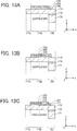
- the lower electrode 210, the piezoelectric part 220, and the upper electrode 230 are formed on the silicon active layer 173 of the first support part 120 and on the silicon active layer 173 between the first support part 120 and the torsion bar 111b in the first piezoelectric actuation part 112b.
- the lower electrode 210, the piezoelectric part 220, and the upper electrode 230 of the first piezoelectric actuation part 112b project above the first support part 120.
- the lower electrode 210, the piezoelectric part 220, and the upper electrode 230 of the first piezoelectric actuation part 112a project above the first support part 120.
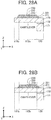
- FIGS. 16A to 16C are top views illustrating an S-region (a region surrounded by a broken line indicated by a reference sign S) in Comparative Examples 1 and 2 and FIG. 12 of this embodiment, respectively.
- S-region a region surrounded by a broken line indicated by a reference sign S
- members having the same structure and function as those of the movable device 13 of this embodiment are denoted by the same reference numerals as those of the movable device 13.
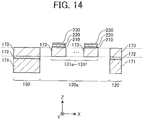
- the lower electrode 210, the piezoelectric part 220, and the upper electrode 230 are formed on the silicon active layer 173 between the corresponding two coupling parts 141bc and 141cd, on the silicon active layer 173 of the coupling part 141bc, and on the silicon active layer 173 of the coupling part 141cd.
- the lower electrode 210, the piezoelectric part 220, and the upper electrode 230 of the second piezoelectric actuation part 131c project above the corresponding two coupling parts 141bc and 141cd.
- the lower electrode 210, the piezoelectric part 220, and the upper electrode 230 of the other second piezoelectric actuation part project above the corresponding two coupling parts.
- a part of the lower electrode 210 on the coupling part (this part is hereinafter also referred to as a "lower electrode projecting part 2") is denoted by reference numeral 211, and a part of the piezoelectric part 220 on the coupling part (this part is hereinafter also referred to as a "piezoelectric part projecting part 2") is denoted by reference numeral 221.
- the lower electrode 210 and the piezoelectric part 220 of the other second piezoelectric actuation part project above the corresponding two coupling parts.
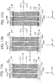
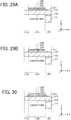
- FIGS. 17A to 17C are top views illustrating a T-region (a region surrounded by a broken line indicated by reference sign T) in FIG. 12 of Comparative Examples 1 and 2 and this embodiment, respectively.
- T-region a region surrounded by a broken line indicated by reference sign T
- members having the same structure and function as those of the movable device 13 of this embodiment are denoted by the same reference numerals as those of the movable device 13.
- the silicon oxide film which is an insulating layer, also functions as an antireflective material.
- the piezoelectric parts 220 of the first drive parts 110a and 110b and the second drive parts 130a and 130b when a positive or negative voltage is applied in a polarization direction, a deformation (for example, expansion and contraction) which is proportional to the potential of the applied voltage occurs, so that a so-called inverse piezoelectric effect is exhibited.
- the first drive parts 110a and 110b and the second drive parts 130a and 130b utilize the above-mentioned inverse piezoelectric effect to allow the silicon active layer 173, which is included in the Z-direction layer structure of the first piezoelectric actuation part and the second piezoelectric actuation part, to be deformed to expand or contract in conjunction with the piezoelectric part 220. This allows the mirror part 101 to be movable.
- the first support part 120 When the first drive parts 110a and 110b are driven to rotate the mirror part 101, the first support part 120 functions as a fixed end of the first piezoelectric actuation part.
- the first support part 120 has a layer that is formed continually with the second piezoelectric actuation part. Therefore, it is not desirable that the drive source of the first piezoelectric actuation part is present on the first support part 120. This is because the silicon active layer 173 of the first support part 120 is continuous with the silicon active layer 173 of the second piezoelectric actuation part. In the case of a two-axis operation, the vibration of the first piezoelectric actuation part becomes vibration crosstalk with respect to the vibration of the second piezoelectric actuation part.
- the deflection angle of the second drive part 130b is zero.
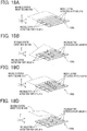
- even-numbered second piezoelectric actuation parts counted from the second piezoelectric actuation part (132a) that is closest to the mirror part, i.e., the second piezoelectric actuation parts 132b, 132d, and 132f, are also defined as the piezoelectric drive part group B.
- the piezoelectric drive part group B When drive voltages are applied in parallel to the piezoelectric drive part group B, as illustrated in FIG. 18D , the piezoelectric drive part group B is deformed to bend in the same direction and thus the mirror part 101 is movable about the second axis in the +Z-direction.
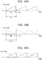
- the sawtooth-shaped waveforms of the drive voltage A and the drive voltage B are generated by superimposing sine waves.
- a drive voltage having a sawtooth-shaped waveform is used as each of the drive voltages A and B, but the drive voltage is not limited to this.
- Drive voltages having a waveform that is changed depending on device characteristics of the movable device such as a drive voltage having a sawtooth-shaped waveform with rounded peaks, and a drive voltage having a waveform obtained by changing a linear region of a sawtooh shape wave into a curve, may also be used.
- the second drive parts cause a plurality of cantilevers to be simultaneously deformed to bend, to accumulate the movable amounts due to bending deformation. Further, the drive signal waveforms to be input to the piezoelectric drive part group A and the piezoelectric drive part group B are controlled to enable non-resonant driving for obtaining a desired deflection angle.
- the piezoelectric part is sandwiched between the upper electrode and the lower electrode, which serves as the drive source. Further, an electric wire is coupled to the drive source to implement a function as a piezoelectric actuator.
- the drive source composed of the piezoelectric part 220, the upper electrode 230, and the lower electrode 210 has a large area, while the presence of the drive source in a member corresponding to a support frame of the drive part may induce an unintended vibration in the first drive part and the second drive part, which may generate vibration crosstalk.
- the piezoelectric actuator (the first piezoelectric actuation part and the second piezoelectric actuation part) of this embodiment described above includes the cantilever (beam) having one end coupled to the first member, and another end coupled to the second member; the lower electrode 210 (first electrode) provided on at least the cantilever; the piezoelectric part 220 (piezoelectric body) provided on the lower electrode 210; and the upper electrode 230 (second electrode) provided on the piezoelectric part 220.
- the lower electrode 210 projects above at least one of the first and second members. Examples of the first and second members include the torsion bars 111a and 111b, the first support part 120, the coupling part, and the second support part 150.
- At least two of the upper electrode 230, the lower electrode 210, and the piezoelectric part 220 have a non-similar shape. That is, at least two of the upper electrode 230, the lower electrode 210, and the piezoelectric part 220 have shapes that are different from each other.
- the torsion bar coupled to one end of the cantilever of the piezoelectric actuator, the support part 120 that supports another end of the cantilever, and the mirror part 101 coupled to the torsion bar, a desired deflection angle can be obtained and a light deflector with high operation reliability can be implemented.
- the optical scanning device (for example, the light writing device 600) of this embodiment is an optical scanning device that scans an object with light, and includes the light source device 12, and the movable device 13 serving as a light deflection element that deflects light from the light source device 12.
- an object can be stably scanned with light with high accuracy.
- the quality of an image formed on the scanned surface 15 can be improved.
Landscapes
- Physics & Mathematics (AREA)
- General Physics & Mathematics (AREA)
- Optics & Photonics (AREA)
- Mechanical Optical Scanning Systems (AREA)
Claims (7)
- Piezoelektrischer Aktuator, enthaltend:einen Balken, der ein an ein Glied gekoppeltes Ende aufweist;eine erste Elektrode (210), die wenigstens auf dem Balken vorgesehen ist;einen piezoelektrischen Körper (220), der auf der ersten Elektrode (210) vorgesehen ist; und eine zweite Elektrode (230), die auf dem piezoelektrischen Körper (220) vorgesehen ist, wobei die erste Elektrode (210) oberhalb des Glieds vorsteht, wodurch sie ein Vorsprungteil (211) der ersten Elektrode (210) definiert, undein Teil der ersten Elektrode (210), der auf dem Balken vorgesehen ist, länger entlang der Richtung des Vorsprungs als das Vorsprungsteil (211) der ersten Elektrode (210) ist und wobei der piezoelektrische Körper (220) oberhalb des Glieds ein Vorsprungteil (221) des piezoelektrischen Körpers (220) definiert; undein Teil des piezoelektrischen Körpers (220) der auf dem Balken vorgesehen ist, länger entlang der Richtung des Vorsprungs als das Vorsprungteil (221) des piezoelektrischen Körpers (220) ist,dadurch gekennzeichnet, dassdie zweite Elektrode nicht oberhalb des Glieds hervorsteht.
- Piezoelektrischer Aktuator gemäß Anspruch 1, bei dem ein Vorsprungteil (211) der ersten Elektrode (210), das oberhalb des Glieds hervorsteht, einen Bereich aufweist, in dem das Vorsprungteil (221) des piezoelektrischen Körpers (220) nicht vorgesehen ist, wobei der Bereich mit einem Draht verbunden ist.
- Piezoelektrischer Aktuator gemäß Anspruch 2, bei dem die erste Elektrode (210) und der piezoelektrische Körper (220) Gestalten aufweisen, die sich voneinander unterscheiden.
- Lichtdeflektor, enthaltend:den piezoelektrischen Aktuator gemäß irgendeinem der Ansprüche 1 bis 3;eine Torsionsstange (111a, 111b, 211a, 211b), die ein Ende aufweist, das an den Balken des piezoelektrischen Aktuators gekoppelt ist;ein Stützteil (120, 150, 250), das an das hintere Ende des Balkens gekoppelt ist; undein Spiegelteil (101), das an die Torsionsstange (111a, 111b, 211a, 211b) gekoppelt ist.
- Lichtdeflektor, enthaltend:ein Antriebssystem, das eine Mehrzahl piezoelektrischer Aktuatoren enthält, wobei jeder piezoelektrische Aktuator der piezoelektrische Aktuator gemäß irgendeinem der Ansprüche 1 bis 3, wobei die Balken der Mehrzahl piezoelektrischer Aktuatoren miteinander durch ein Kopplungsteil (141ab bis 141ef, 142ab bis 142ef) so gekoppelt sind, dass sie insgesamt eine Meanderstruktur bilden;ein bewegliches System, das an ein Ende des Antriebssystems gekoppelt ist und ein Spiegelteil (101) enthält; undein Stützteil (120, 150, 250), das eingerichtet ist, ein anderes Ende des Antriebssystems zu stützen.
- Lichtreflektor gemäß Anspruch 5, bei dem
das bewegliche System ferner enthält:eine Torsionsstange (111a, 111b, 211a, 211b), die mit dem Spiegelteil (101) gekoppelt ist;den piezoelektrischen Aktuator gemäß irgendeinem der Ansprüche 1 bis 6, wobei ein Ende des Balkens mit der Torsionsstange (111a, 111b, 211a, 211b) gekoppelt ist; undein anderes Stützteil (120, 150, 250), das mit einem anderen Ende des Balkens gekoppelt ist. - Bildprojektionsvorrichtung, enthaltend:eine Lichtquellenvorrichtung (12);den Lichtdeflektor gemäß irgendeinem der Ansprüche 4 bis 5, wobei der Lichtdeflektor eingerichtet ist, Licht von der Lichtquellenvorrichtung (12) abzulenken;einen Bildschirm (510), auf dem durch den Lichtdeflektor hindurchgehendes Licht emittiert wird, um ein Bild zu bilden; undein optisches System (511), das eingerichtet ist, Licht durch den Bildschirm (510) hindurch zu projizieren.
Applications Claiming Priority (2)
| Application Number | Priority Date | Filing Date | Title |
|---|---|---|---|
| JP2016128760 | 2016-06-29 | ||
| JP2017083532A JP6926625B2 (ja) | 2016-06-29 | 2017-04-20 | 圧電アクチュエータ、光偏向器及び画像投影装置 |
Publications (2)
| Publication Number | Publication Date |
|---|---|
| EP3264155A1 EP3264155A1 (de) | 2018-01-03 |
| EP3264155B1 true EP3264155B1 (de) | 2020-09-23 |
Family
ID=59284996
Family Applications (1)
| Application Number | Title | Priority Date | Filing Date |
|---|---|---|---|
| EP17178097.6A Active EP3264155B1 (de) | 2016-06-29 | 2017-06-27 | Piezoelektrisches aktuator, lichtablenker und bildprojektionsvorrichtung |
Country Status (1)
| Country | Link |
|---|---|
| EP (1) | EP3264155B1 (de) |
Families Citing this family (2)
| Publication number | Priority date | Publication date | Assignee | Title |
|---|---|---|---|---|
| WO2022014471A1 (ja) | 2020-07-16 | 2022-01-20 | 富士フイルム株式会社 | 光走査装置、及びマイクロミラーデバイスの駆動方法 |
| IT202200004745A1 (it) * | 2022-03-11 | 2023-09-11 | St Microelectronics Srl | Dispositivo microelettromeccanico di specchio biassiale con attuazione piezoelettrica |
Citations (1)
| Publication number | Priority date | Publication date | Assignee | Title |
|---|---|---|---|---|
| US20150062683A1 (en) * | 2012-11-15 | 2015-03-05 | Goichi Akanuma | Optical deflection device and image forming apparatus |
Family Cites Families (3)
| Publication number | Priority date | Publication date | Assignee | Title |
|---|---|---|---|---|
| JP5391600B2 (ja) * | 2008-07-16 | 2014-01-15 | 船井電機株式会社 | 振動ミラー素子 |
| JP5728823B2 (ja) * | 2009-06-09 | 2015-06-03 | 株式会社リコー | 光偏向器、光走査装置、画像形成装置及び画像投影装置 |
| WO2012111332A1 (ja) | 2011-02-17 | 2012-08-23 | パナソニック株式会社 | ミアンダ型振動子および光学反射素子 |
-
2017
- 2017-06-27 EP EP17178097.6A patent/EP3264155B1/de active Active
Patent Citations (1)
| Publication number | Priority date | Publication date | Assignee | Title |
|---|---|---|---|---|
| US20150062683A1 (en) * | 2012-11-15 | 2015-03-05 | Goichi Akanuma | Optical deflection device and image forming apparatus |
Also Published As
| Publication number | Publication date |
|---|---|
| EP3264155A1 (de) | 2018-01-03 |
Similar Documents
| Publication | Publication Date | Title |
|---|---|---|
| EP3494433B1 (de) | Lichtablenker, optische abtastvorrichtung, bildprojektionsvorrichtung und mobiles objekt | |
| JP7363177B2 (ja) | 光偏向器、光走査システム、画像投影装置、画像形成装置、レーザレーダ | |
| CN107203037B (zh) | 控制装置、光偏转系统、图像投影装置以及控制方法 | |
| US11750779B2 (en) | Light deflector, optical scanning system, image projection device, image forming apparatus, and lidar device | |
| US10831024B2 (en) | Optical scanning apparatus, image projecting apparatus, and mobile object | |
| JP7172557B2 (ja) | 光偏向装置、画像投影装置、レーザヘッドランプ及び移動体 | |
| JP6915292B2 (ja) | 制御装置、光偏向システム、画像投影装置、車両、移動体、非移動体、光書込装置、物体認識装置及び制御方法 | |
| JP2021063905A (ja) | 光偏向器、偏向装置、距離測定装置、画像投影装置、及び車両 | |
| JP7639424B2 (ja) | 可動装置、画像投影装置、ヘッドアップディスプレイ、レーザヘッドランプ、ヘッドマウントディスプレイ、距離測定装置、及び移動体 | |
| JP6926625B2 (ja) | 圧電アクチュエータ、光偏向器及び画像投影装置 | |
| JP2020101588A (ja) | 可動装置、距離測定装置、画像投影装置、車両、及び台座 | |
| KR102178800B1 (ko) | 제어 장치, 화상 투영 장치, 및 제어 방법 | |
| JP2020101587A (ja) | 可動装置、距離測定装置、画像投影装置、及び車両 | |
| JP7593186B2 (ja) | 光偏向器、画像投影装置、ヘッドアップディスプレイ、レーザヘッドランプ、ヘッドマウントディスプレイ、距離測定装置、及び移動体 | |
| JP2018022004A (ja) | 光偏向器、画像表示システム | |
| EP3264155A1 (de) | Piezoelektrisches aktuator, lichtablenker und bildprojektionsvorrichtung | |
| JP2020190620A (ja) | 光偏向装置、画像投影装置、車両、及び調整方法 | |
| JP2018013546A (ja) | 光偏向器、光走査装置、画像投影装置および画像形成装置 | |
| JP7468173B2 (ja) | 光偏向器、光走査システム、画像投影装置、画像形成装置、レーザレーダ | |
| JP6809281B2 (ja) | 光偏向器及び光走査装置及び画像投影装置及び物体認識装置 | |
| JP7247553B2 (ja) | 可動装置、画像投影装置、ヘッドアップディスプレイ、レーザヘッドランプ、ヘッドマウントディスプレイ、物体認識装置、及び車両 | |
| JP6703746B2 (ja) | 光偏向素子、光走査装置及び画像投影装置 | |
| JP2018005201A (ja) | アクチュエータ装置、アクチュエータシステム | |
| JP2025130475A (ja) | 可動装置、画像投影装置、ヘッドアップディスプレイ、レーザヘッドランプ、ヘッドマウントディスプレイ、物体認識装置、及び移動体 | |
| JP2023005225A (ja) | 半導体デバイスおよび半導体デバイスの製造方法 |
Legal Events
| Date | Code | Title | Description |
|---|---|---|---|
| PUAI | Public reference made under article 153(3) epc to a published international application that has entered the european phase |
Free format text: ORIGINAL CODE: 0009012 |
|
| STAA | Information on the status of an ep patent application or granted ep patent |
Free format text: STATUS: REQUEST FOR EXAMINATION WAS MADE |
|
| 17P | Request for examination filed |
Effective date: 20170627 |
|
| AK | Designated contracting states |
Kind code of ref document: A1 Designated state(s): AL AT BE BG CH CY CZ DE DK EE ES FI FR GB GR HR HU IE IS IT LI LT LU LV MC MK MT NL NO PL PT RO RS SE SI SK SM TR |
|
| AX | Request for extension of the european patent |
Extension state: BA ME |
|
| STAA | Information on the status of an ep patent application or granted ep patent |
Free format text: STATUS: EXAMINATION IS IN PROGRESS |
|
| 17Q | First examination report despatched |
Effective date: 20191128 |
|
| GRAP | Despatch of communication of intention to grant a patent |
Free format text: ORIGINAL CODE: EPIDOSNIGR1 |
|
| STAA | Information on the status of an ep patent application or granted ep patent |
Free format text: STATUS: GRANT OF PATENT IS INTENDED |
|
| INTG | Intention to grant announced |
Effective date: 20200602 |
|
| RIN1 | Information on inventor provided before grant (corrected) |
Inventor name: SUZUKI, SHUICHI Inventor name: SHINKAWA, MIZUKI |
|
| GRAS | Grant fee paid |
Free format text: ORIGINAL CODE: EPIDOSNIGR3 |
|
| GRAA | (expected) grant |
Free format text: ORIGINAL CODE: 0009210 |
|
| STAA | Information on the status of an ep patent application or granted ep patent |
Free format text: STATUS: THE PATENT HAS BEEN GRANTED |
|
| AK | Designated contracting states |
Kind code of ref document: B1 Designated state(s): AL AT BE BG CH CY CZ DE DK EE ES FI FR GB GR HR HU IE IS IT LI LT LU LV MC MK MT NL NO PL PT RO RS SE SI SK SM TR |
|
| REG | Reference to a national code |
Ref country code: GB Ref legal event code: FG4D |
|
| REG | Reference to a national code |
Ref country code: CH Ref legal event code: EP |
|
| REG | Reference to a national code |
Ref country code: DE Ref legal event code: R096 Ref document number: 602017024004 Country of ref document: DE |
|
| REG | Reference to a national code |
Ref country code: IE Ref legal event code: FG4D |
|
| REG | Reference to a national code |
Ref country code: AT Ref legal event code: REF Ref document number: 1316983 Country of ref document: AT Kind code of ref document: T Effective date: 20201015 |
|
| PG25 | Lapsed in a contracting state [announced via postgrant information from national office to epo] |
Ref country code: FI Free format text: LAPSE BECAUSE OF FAILURE TO SUBMIT A TRANSLATION OF THE DESCRIPTION OR TO PAY THE FEE WITHIN THE PRESCRIBED TIME-LIMIT Effective date: 20200923 Ref country code: SE Free format text: LAPSE BECAUSE OF FAILURE TO SUBMIT A TRANSLATION OF THE DESCRIPTION OR TO PAY THE FEE WITHIN THE PRESCRIBED TIME-LIMIT Effective date: 20200923 Ref country code: HR Free format text: LAPSE BECAUSE OF FAILURE TO SUBMIT A TRANSLATION OF THE DESCRIPTION OR TO PAY THE FEE WITHIN THE PRESCRIBED TIME-LIMIT Effective date: 20200923 Ref country code: GR Free format text: LAPSE BECAUSE OF FAILURE TO SUBMIT A TRANSLATION OF THE DESCRIPTION OR TO PAY THE FEE WITHIN THE PRESCRIBED TIME-LIMIT Effective date: 20201224 Ref country code: BG Free format text: LAPSE BECAUSE OF FAILURE TO SUBMIT A TRANSLATION OF THE DESCRIPTION OR TO PAY THE FEE WITHIN THE PRESCRIBED TIME-LIMIT Effective date: 20201223 Ref country code: NO Free format text: LAPSE BECAUSE OF FAILURE TO SUBMIT A TRANSLATION OF THE DESCRIPTION OR TO PAY THE FEE WITHIN THE PRESCRIBED TIME-LIMIT Effective date: 20201223 |
|
| REG | Reference to a national code |
Ref country code: AT Ref legal event code: MK05 Ref document number: 1316983 Country of ref document: AT Kind code of ref document: T Effective date: 20200923 |
|
| PG25 | Lapsed in a contracting state [announced via postgrant information from national office to epo] |
Ref country code: RS Free format text: LAPSE BECAUSE OF FAILURE TO SUBMIT A TRANSLATION OF THE DESCRIPTION OR TO PAY THE FEE WITHIN THE PRESCRIBED TIME-LIMIT Effective date: 20200923 Ref country code: LV Free format text: LAPSE BECAUSE OF FAILURE TO SUBMIT A TRANSLATION OF THE DESCRIPTION OR TO PAY THE FEE WITHIN THE PRESCRIBED TIME-LIMIT Effective date: 20200923 |
|
| REG | Reference to a national code |
Ref country code: NL Ref legal event code: MP Effective date: 20200923 |
|
| REG | Reference to a national code |
Ref country code: LT Ref legal event code: MG4D |
|
| PG25 | Lapsed in a contracting state [announced via postgrant information from national office to epo] |
Ref country code: EE Free format text: LAPSE BECAUSE OF FAILURE TO SUBMIT A TRANSLATION OF THE DESCRIPTION OR TO PAY THE FEE WITHIN THE PRESCRIBED TIME-LIMIT Effective date: 20200923 Ref country code: SM Free format text: LAPSE BECAUSE OF FAILURE TO SUBMIT A TRANSLATION OF THE DESCRIPTION OR TO PAY THE FEE WITHIN THE PRESCRIBED TIME-LIMIT Effective date: 20200923 Ref country code: PT Free format text: LAPSE BECAUSE OF FAILURE TO SUBMIT A TRANSLATION OF THE DESCRIPTION OR TO PAY THE FEE WITHIN THE PRESCRIBED TIME-LIMIT Effective date: 20210125 Ref country code: RO Free format text: LAPSE BECAUSE OF FAILURE TO SUBMIT A TRANSLATION OF THE DESCRIPTION OR TO PAY THE FEE WITHIN THE PRESCRIBED TIME-LIMIT Effective date: 20200923 Ref country code: CZ Free format text: LAPSE BECAUSE OF FAILURE TO SUBMIT A TRANSLATION OF THE DESCRIPTION OR TO PAY THE FEE WITHIN THE PRESCRIBED TIME-LIMIT Effective date: 20200923 Ref country code: LT Free format text: LAPSE BECAUSE OF FAILURE TO SUBMIT A TRANSLATION OF THE DESCRIPTION OR TO PAY THE FEE WITHIN THE PRESCRIBED TIME-LIMIT Effective date: 20200923 |
|
| PG25 | Lapsed in a contracting state [announced via postgrant information from national office to epo] |
Ref country code: AT Free format text: LAPSE BECAUSE OF FAILURE TO SUBMIT A TRANSLATION OF THE DESCRIPTION OR TO PAY THE FEE WITHIN THE PRESCRIBED TIME-LIMIT Effective date: 20200923 Ref country code: AL Free format text: LAPSE BECAUSE OF FAILURE TO SUBMIT A TRANSLATION OF THE DESCRIPTION OR TO PAY THE FEE WITHIN THE PRESCRIBED TIME-LIMIT Effective date: 20200923 Ref country code: ES Free format text: LAPSE BECAUSE OF FAILURE TO SUBMIT A TRANSLATION OF THE DESCRIPTION OR TO PAY THE FEE WITHIN THE PRESCRIBED TIME-LIMIT Effective date: 20200923 Ref country code: IS Free format text: LAPSE BECAUSE OF FAILURE TO SUBMIT A TRANSLATION OF THE DESCRIPTION OR TO PAY THE FEE WITHIN THE PRESCRIBED TIME-LIMIT Effective date: 20210123 Ref country code: PL Free format text: LAPSE BECAUSE OF FAILURE TO SUBMIT A TRANSLATION OF THE DESCRIPTION OR TO PAY THE FEE WITHIN THE PRESCRIBED TIME-LIMIT Effective date: 20200923 |
|
| REG | Reference to a national code |
Ref country code: DE Ref legal event code: R097 Ref document number: 602017024004 Country of ref document: DE |
|
| PG25 | Lapsed in a contracting state [announced via postgrant information from national office to epo] |
Ref country code: SK Free format text: LAPSE BECAUSE OF FAILURE TO SUBMIT A TRANSLATION OF THE DESCRIPTION OR TO PAY THE FEE WITHIN THE PRESCRIBED TIME-LIMIT Effective date: 20200923 |
|
| PLBE | No opposition filed within time limit |
Free format text: ORIGINAL CODE: 0009261 |
|
| STAA | Information on the status of an ep patent application or granted ep patent |
Free format text: STATUS: NO OPPOSITION FILED WITHIN TIME LIMIT |
|
| PG25 | Lapsed in a contracting state [announced via postgrant information from national office to epo] |
Ref country code: DK Free format text: LAPSE BECAUSE OF FAILURE TO SUBMIT A TRANSLATION OF THE DESCRIPTION OR TO PAY THE FEE WITHIN THE PRESCRIBED TIME-LIMIT Effective date: 20200923 Ref country code: SI Free format text: LAPSE BECAUSE OF FAILURE TO SUBMIT A TRANSLATION OF THE DESCRIPTION OR TO PAY THE FEE WITHIN THE PRESCRIBED TIME-LIMIT Effective date: 20200923 |
|
| 26N | No opposition filed |
Effective date: 20210624 |
|
| PG25 | Lapsed in a contracting state [announced via postgrant information from national office to epo] |
Ref country code: IT Free format text: LAPSE BECAUSE OF FAILURE TO SUBMIT A TRANSLATION OF THE DESCRIPTION OR TO PAY THE FEE WITHIN THE PRESCRIBED TIME-LIMIT Effective date: 20200923 |
|
| PG25 | Lapsed in a contracting state [announced via postgrant information from national office to epo] |
Ref country code: MC Free format text: LAPSE BECAUSE OF FAILURE TO SUBMIT A TRANSLATION OF THE DESCRIPTION OR TO PAY THE FEE WITHIN THE PRESCRIBED TIME-LIMIT Effective date: 20200923 |
|
| REG | Reference to a national code |
Ref country code: CH Ref legal event code: PL |
|
| REG | Reference to a national code |
Ref country code: BE Ref legal event code: MM Effective date: 20210630 |
|
| PG25 | Lapsed in a contracting state [announced via postgrant information from national office to epo] |
Ref country code: LU Free format text: LAPSE BECAUSE OF NON-PAYMENT OF DUE FEES Effective date: 20210627 |
|
| PG25 | Lapsed in a contracting state [announced via postgrant information from national office to epo] |
Ref country code: LI Free format text: LAPSE BECAUSE OF NON-PAYMENT OF DUE FEES Effective date: 20210630 Ref country code: IE Free format text: LAPSE BECAUSE OF NON-PAYMENT OF DUE FEES Effective date: 20210627 Ref country code: CH Free format text: LAPSE BECAUSE OF NON-PAYMENT OF DUE FEES Effective date: 20210630 |
|
| PG25 | Lapsed in a contracting state [announced via postgrant information from national office to epo] |
Ref country code: BE Free format text: LAPSE BECAUSE OF NON-PAYMENT OF DUE FEES Effective date: 20210630 |
|
| PG25 | Lapsed in a contracting state [announced via postgrant information from national office to epo] |
Ref country code: HU Free format text: LAPSE BECAUSE OF FAILURE TO SUBMIT A TRANSLATION OF THE DESCRIPTION OR TO PAY THE FEE WITHIN THE PRESCRIBED TIME-LIMIT; INVALID AB INITIO Effective date: 20170627 |
|
| P01 | Opt-out of the competence of the unified patent court (upc) registered |
Effective date: 20230522 |
|
| PG25 | Lapsed in a contracting state [announced via postgrant information from national office to epo] |
Ref country code: NL Free format text: LAPSE BECAUSE OF NON-PAYMENT OF DUE FEES Effective date: 20200923 Ref country code: CY Free format text: LAPSE BECAUSE OF FAILURE TO SUBMIT A TRANSLATION OF THE DESCRIPTION OR TO PAY THE FEE WITHIN THE PRESCRIBED TIME-LIMIT Effective date: 20200923 |
|
| PG25 | Lapsed in a contracting state [announced via postgrant information from national office to epo] |
Ref country code: MK Free format text: LAPSE BECAUSE OF FAILURE TO SUBMIT A TRANSLATION OF THE DESCRIPTION OR TO PAY THE FEE WITHIN THE PRESCRIBED TIME-LIMIT Effective date: 20200923 |
|
| PG25 | Lapsed in a contracting state [announced via postgrant information from national office to epo] |
Ref country code: MT Free format text: LAPSE BECAUSE OF FAILURE TO SUBMIT A TRANSLATION OF THE DESCRIPTION OR TO PAY THE FEE WITHIN THE PRESCRIBED TIME-LIMIT Effective date: 20200923 |
|
| PG25 | Lapsed in a contracting state [announced via postgrant information from national office to epo] |
Ref country code: TR Free format text: LAPSE BECAUSE OF FAILURE TO SUBMIT A TRANSLATION OF THE DESCRIPTION OR TO PAY THE FEE WITHIN THE PRESCRIBED TIME-LIMIT Effective date: 20200923 |
|
| PGFP | Annual fee paid to national office [announced via postgrant information from national office to epo] |
Ref country code: GB Payment date: 20260625 Year of fee payment: 10 |
|
| PGFP | Annual fee paid to national office [announced via postgrant information from national office to epo] |
Ref country code: DE Payment date: 20260622 Year of fee payment: 10 |
|
| PGFP | Annual fee paid to national office [announced via postgrant information from national office to epo] |
Ref country code: FR Payment date: 20260626 Year of fee payment: 10 |