EP3264276A1 - Vorrichtung zur steuerung des zugangs zu einer speichervorrichtung und verfahren zur durchführung von wartungsarbeiten in solch einer vorrichtung - Google Patents
Vorrichtung zur steuerung des zugangs zu einer speichervorrichtung und verfahren zur durchführung von wartungsarbeiten in solch einer vorrichtung Download PDFInfo
- Publication number
- EP3264276A1 EP3264276A1 EP16176680.3A EP16176680A EP3264276A1 EP 3264276 A1 EP3264276 A1 EP 3264276A1 EP 16176680 A EP16176680 A EP 16176680A EP 3264276 A1 EP3264276 A1 EP 3264276A1
- Authority
- EP
- European Patent Office
- Prior art keywords
- maintenance
- circuitry
- training
- physical layer
- memory device
- Prior art date
- Legal status (The legal status is an assumption and is not a legal conclusion. Google has not performed a legal analysis and makes no representation as to the accuracy of the status listed.)
- Withdrawn
Links
Images



Classifications
-
- G—PHYSICS
- G06—COMPUTING OR CALCULATING; COUNTING
- G06F—ELECTRIC DIGITAL DATA PROCESSING
- G06F13/00—Interconnection of, or transfer of information or other signals between, memories, input/output devices or central processing units
- G06F13/14—Handling requests for interconnection or transfer
- G06F13/16—Handling requests for interconnection or transfer for access to memory bus
- G06F13/1605—Handling requests for interconnection or transfer for access to memory bus based on arbitration
- G06F13/161—Handling requests for interconnection or transfer for access to memory bus based on arbitration with latency improvement
-
- G—PHYSICS
- G06—COMPUTING OR CALCULATING; COUNTING
- G06F—ELECTRIC DIGITAL DATA PROCESSING
- G06F11/00—Error detection; Error correction; Monitoring
- G06F11/22—Detection or location of defective computer hardware by testing during standby operation or during idle time, e.g. start-up testing
-
- G—PHYSICS
- G06—COMPUTING OR CALCULATING; COUNTING
- G06F—ELECTRIC DIGITAL DATA PROCESSING
- G06F11/00—Error detection; Error correction; Monitoring
- G06F11/07—Responding to the occurrence of a fault, e.g. fault tolerance
- G06F11/08—Error detection or correction by redundancy in data representation, e.g. by using checking codes
- G06F11/10—Adding special bits or symbols to the coded information, e.g. parity check, casting out 9's or 11's
- G06F11/1008—Adding special bits or symbols to the coded information, e.g. parity check, casting out 9's or 11's in individual solid state devices
- G06F11/1064—Adding special bits or symbols to the coded information, e.g. parity check, casting out 9's or 11's in individual solid state devices in cache or content addressable memories
-
- G—PHYSICS
- G06—COMPUTING OR CALCULATING; COUNTING
- G06F—ELECTRIC DIGITAL DATA PROCESSING
- G06F11/00—Error detection; Error correction; Monitoring
- G06F11/30—Monitoring
- G06F11/3003—Monitoring arrangements specially adapted to the computing system or computing system component being monitored
- G06F11/3037—Monitoring arrangements specially adapted to the computing system or computing system component being monitored where the computing system component is a memory, e.g. virtual memory, cache
-
- G—PHYSICS
- G06—COMPUTING OR CALCULATING; COUNTING
- G06F—ELECTRIC DIGITAL DATA PROCESSING
- G06F13/00—Interconnection of, or transfer of information or other signals between, memories, input/output devices or central processing units
- G06F13/14—Handling requests for interconnection or transfer
- G06F13/16—Handling requests for interconnection or transfer for access to memory bus
- G06F13/1668—Details of memory controller
- G06F13/1673—Details of memory controller using buffers
-
- G—PHYSICS
- G11—INFORMATION STORAGE
- G11C—STATIC STORES
- G11C29/00—Checking stores for correct operation ; Subsequent repair; Testing stores during standby or offline operation
- G11C29/04—Detection or location of defective memory elements, e.g. cell constructio details, timing of test signals
- G11C29/08—Functional testing, e.g. testing during refresh, power-on self testing [POST] or distributed testing
- G11C29/12—Built-in arrangements for testing, e.g. built-in self testing [BIST] or interconnection details
-
- G—PHYSICS
- G11—INFORMATION STORAGE
- G11C—STATIC STORES
- G11C2207/00—Indexing scheme relating to arrangements for writing information into, or reading information out from, a digital store
- G11C2207/22—Control and timing of internal memory operations
- G11C2207/2254—Calibration
Definitions
- the present technique relates to an apparatus for controlling access to a memory device, and to a method of performing a maintenance operation within such an apparatus.
- An apparatus used to control access to a memory device may receive access requests from a number of sources and may have access to a storage device in which the access requests to be issued to the memory device can be buffered.
- an apparatus for controlling access to a memory device comprising: a storage device to store access requests to be issued to the memory device; maintenance circuitry to perform a maintenance operation on storage elements provided within the storage device; memory access execution circuitry to issue to a physical layer interface access requests selected from the storage device, for onward propagation from the physical layer interface to the memory device; and control circuitry, responsive to a training event, to initiate a training operation of the physical layer interface; the control circuitry further being responsive to the training event to trigger performance of the maintenance operation by the maintenance circuitry whilst the training operation is being performed.
- a method of performing a maintenance operation within an apparatus that controls access to a memory device comprising: storing in a storage device access requests to be issued to the memory device; employing maintenance circuitry to perform the maintenance operation on storage elements provided within the storage device; issuing to a physical layer interface access requests selected from the storage device, for onward propagation from the physical layer interface to the memory device; responsive to a training event, employing control circuitry to initiate a training operation of the physical layer interface; and causing the control circuitry to trigger performance of the maintenance operation by the maintenance circuitry whilst the training operation is being performed.
- an apparatus for controlling access to a memory device comprising: storage means for storing access requests to be issued to the memory device; maintenance means for performing a maintenance operation on storage elements provided within the storage means; memory access execution means for issuing to a physical layer interface access requests selected from the storage means, for onward propagation from the physical layer interface to the memory device; and control means for initiating, responsive to a training event, a training operation of the physical layer interface; the control means further for triggering, in response to the training event, performance of the maintenance operation by the maintenance means whilst the training operation is being performed.
- a number of components of the system may be integrated together on-chip and one or more of the components may need to communicate with a memory device.
- the memory device can take a variety of forms, one example being Dynamic Random Access Memory (DRAM), and in modern systems the storage capacity may be quite large.
- DRAM Dynamic Random Access Memory
- the memory device itself may be provided off-chip, with an on-chip memory controller being used to control access to that memory device.
- the memory controller will typically have access to a storage device in which the access requests to be issued to the memory device can be buffered.
- Such tasks could be performed as a background operation, but there will be contention for the access bandwidth to the storage device between the normal read/write activity in the storage device required when processing the access requests in order to perform the accesses to the memory device, and the read/write activity in the storage device that is needed in order to perform the required maintenance tasks.
- Such background maintenance tasks hence have the potential to impact performance, particularly as the size of the storage device, and hence the number of storage elements to be subjected to maintenance, increases.
- BIST built-in self-test
- Other types of maintenance operation may also be desired to be performed.
- BIST operations can be performed to check correct operation of the storage elements, and in particular detect when hard errors are present. Whilst traditionally such BIST tasks might only be performed as part of a manufacturing test, or at boot time, in certain applications, such as applications that are highly error intolerant, it may be desirable to also allow such BIST tests to be performed as maintenance operations during live use of the memory controller. However, the performance of such maintenance operations is then likely to impact on the overall performance of the apparatus.
- the embodiments described herein seek to provide an improved technique for handling such maintenance operations.
- an apparatus for controlling access to a memory device, the apparatus having a storage device to store access requests to be issued to the memory device, and maintenance circuitry to perform a maintenance operation on storage elements provided within the storage device.
- Memory access execution circuitry is also provided for issuing to the memory device access requests selected from the storage device.
- the issuance of the access requests occurs via an intervening physical layer interface which receives the access requests from the memory access execution circuitry and manages the onward propagation of the access requests to the memory device.
- the physical layer interface is provided for managing the communication with the memory device taking into account the nature of the physical connection with the memory device. That physical connection will typically comprise multiple relatively long physical wire connections, and be required to operate as a parallel interface at high speed.
- the physical layer interface operates in a manner to maintain synchronised communication across that physical connection with the memory device.
- control circuitry may be provided that is responsive to a training event to initiate a training operation of the physical layer interface.
- the training event can take a variety of forms, for example the elapse of a periodic timer, or the indication of an approaching error condition, for example by analysis of one or more properties of the signals being passed over the physical connection between the physical layer interface and the memory device.
- control circuitry is responsive to the training event to trigger performance of the maintenance operation by the maintenance circuitry whilst the training operation is being performed.
- the maintenance operation is hence performed at a time when the pending access requests cannot in any event be processed, and accordingly the performance of the maintenance operations during that period provides no further impact on the memory access performance.
- This hence provides a very efficient mechanism for facilitating performance of the maintenance operations, by triggering performance of those maintenance operations during a period where there is already a "downtime" in the memory access functionality due to the training operation being performed on the physical layer interface.
- This can be particularly beneficial in situations where the amount of maintenance tasks desired to be performed are at a level where they could impact the overall performance of the memory access operations by introducing a source of contention for access to the storage elements.
- those storage elements will need accessing whilst performing the normal processing of the pending access requests in order to access the required data in the memory device, and if the maintenance operations are at the same time also needing to access the storage elements this can compromise performance, particularly as the volume of maintenance tasks required increases.
- control circuitry can trigger performance of the maintenance operation by the maintenance circuitry in response to the training event.
- control circuitry may in one embodiment be arranged to issue a control signal to the maintenance circuitry to trigger the performance of the maintenance operation.
- control circuitry may be able to directly contact the maintenance circuitry in order to trigger the performance of a maintenance operation.
- control circuitry may not directly contact the maintenance circuitry, but could instead perform an alternative action that would trigger performance of the maintenance operation.
- the control circuitry may be responsive to the training event to update a control register to a value that triggers the maintenance circuitry to perform the maintenance operation.
- the control register may be arranged such that when its value is updated to a predetermined value, this causes an interrupt to occur, that may for instance cause an exception routine to be performed that triggers performance of the maintenance operation.
- the control circuitry can be responsive to the training event to update the control register value to that predetermined value, to thus initiate the interrupt mechanism to trigger performance of the maintenance operation.
- the control circuitry can in one embodiment be arranged to issue an indication of an expected duration of the training operation, and the maintenance circuitry may then be arranged to reference that indication when determining the storage elements to be subjected to the maintenance operation.
- the maintenance circuitry can be informed of the length of time available during which the maintenance operation can be performed without any impact on data access performance, since it is known that there will be no data accesses taking place to the memory device in respect of pending access requests whilst the training operation is being performed.
- the indication of the expected duration of the training operation that is provided by the control circuitry can take a variety of forms. For instance, it could directly identify the time period concerned, for example by reference to a number of clock cycles. Alternatively, it may be sufficient to identify the type of training that is being performed by the training operation. In particular, dependent on the nature of the training event, the type of training that needs to be performed may differ, and different types of training may have different expected durations.
- the maintenance circuitry can be arranged to have access to stored timing information identifying the expected duration of the training operation for each of a plurality of different types of training. In that event, the indication issued by the control circuitry when triggering the maintenance operation may be arranged to provide an indication of the type of training being performed by the training operation, with the maintenance circuitry then using this information to determine the time available for performing maintenance tasks.
- control circuitry may not provide any timing indication information and instead may be arranged to notify the maintenance circuitry on completion of the training operation.
- the maintenance circuitry can then continue to perform maintenance tasks until such time as it is notified that the training operation has completed. It can for example be responsive to that information to terminate the maintenance operation at the next suitable point, for example when any maintenance task in flight at the time the maintenance circuitry is advised of the completion of the training operation has completed.
- the maintenance circuitry when the maintenance operation is triggered by the control circuitry, the maintenance circuitry may be arranged to perform the maintenance operation for a default period of time.
- the default period of time could be selected in a variety of ways, but could for example correspond with a minimum expected duration of the training operation.
- the control circuitry can take a variety of forms. In one embodiment, it may take the form of a dedicated hardware circuit configured to perform the training operation. That hardware circuit will then additionally be configured to issue a signal to trigger performance of the maintenance operation when the training operation is initiated. However, in an alternative embodiment, the control circuitry may take the form of a more general purpose processing circuit that is arranged to execute firmware to perform the training operation. The firmware will then also cause the necessary signal to be issued to trigger performance of the maintenance operation when the training operation is initiated.
- control circuitry is a dedicated hardware circuit
- that dedicated hardware circuit may be provided with a specific path via which it can issue a trigger signal directly to the maintenance circuitry to initiate the maintenance operation.
- control circuitry takes the form of more general purpose processing circuitry executing firmware
- that processing circuitry may be connected via a peripheral bus to various other components within the system, including some control registers used to control operation of components within the system.
- One of those control registers may be arranged to be a register that, when set to a particular value, triggers an interrupt that then causes the maintenance operation to be initiated.
- the storage device containing storage elements that are to be subjected to the maintenance operation can take a variety of forms.
- the storage device comprises a pending access requests buffer, and at least the data portions of the access requests are stored in the storage elements subjected to the maintenance operation.
- the data portions of the access requests may be stored in Static Random Access Memory (SRAM) cells within the storage device, and those SRAM cells may be subjected to the maintenance operation.
- the storage device may use other structures for storing other parts of the request. For example, flops may be used to store the command/address information associated with each access request.
- Such storage structures may not need to be subjected to the maintenance operation, and hence it may not be the entirety of the storage device that is subjected to the maintenance operation.
- all of the information of each access request may be stored in SRAM cells, including the command/address information, and all of those SRAM cells may be subjected to the maintenance operation.
- the storage device may comprise other components, for example a cache structure, and at least a portion of the cache structure may be formed from storage elements subjected to the maintenance operation.
- a cache structure For example, within a System-on-Chip (SoC), a final level cache may be quite closely coupled with the memory controller functionality, and hence regions of the cache may be used for holding access request information.
- accesses to such a cache structure may significantly reduce, or stop, during periods where the physical layer interface is being subjected to the training operation, due to the fact that no active access requests are processed during that period. This period hence also represents a suitable period of time for performing maintenance tasks in respect of the storage elements within the cache structure, and accordingly the trigger from the control circuitry can be propagated on to such a cache structure to initiate those maintenance tasks during that period.
- the maintenance operation can take a variety of forms.
- the maintenance circuitry comprises a built-in self-test (BIST) controller arranged to perform the maintenance operation in order to provide error robustness maintenance.
- BIST built-in self-test
- the maintenance operation performed by the BIST controller may seek to determine the presence of any hard errors in the storage elements. For example, for a series of storage elements used to store one or more data values, that one or more data values may be temporarily buffered elsewhere, and then a series of write and read accesses may be performed to that series of storage elements using known patterns in order to seek to detect any situation where the read pattern differs from the written pattern, and hence may indicate a hard fault.
- the maintenance circuitry may comprise scheduling circuitry arranged to perform the maintenance operation in order to improve performance of the memory accesses identified by the access requests.
- the maintenance operation performed by the scheduling circuitry can seek to use techniques such as access request merging, and scheduling/reordering techniques to seek to optimise performance of memory accesses. Whilst such maintenance can be performed as a background task during live use of the system, the time taken to perform such maintenance can increase as the size of the storage device increases, and hence there is the potential for the performance of such background maintenance tasks to either impact performance of the actual access request processing, due to the contention they introduce in access to the storage elements, or for the scheduling circuitry to struggle to find sufficient time to perform the desired maintenance tasks.
- the maintenance circuitry can perform such maintenance tasks without introducing any contention with respect to the live data access traffic. It hence, for example, can increase the aggressiveness of the maintenance tasks during such a period, by increasing the rate at which the storage elements are subjected to maintenance during that period when the training operation is being performed. This can be done without any risk of impacting performance of the memory access activity, due to memory access activity in any event having been halted during the period where the physical layer interface training is taking place.
- the training operation can take a variety of forms. However, in one embodiment the training operation adjusts operation of the physical layer interface to compensate for delay in signals propagating over a connection between the physical layer interface and the memory device.
- the present technique provides a method of performing a maintenance operation within an apparatus that controls access to a memory device, comprising: storing in a storage device access requests to be issued to the memory device; employing maintenance circuitry to perform the maintenance operation on storage elements provided within the storage device; issuing to a physical layer interface access requests selected from the storage device, for onward propagation from the physical layer interface to the memory device; responsive to a training event, employing control circuitry to initiate a training operation of the physical layer interface; and causing the control circuitry to trigger performance of the maintenance operation by the maintenance circuitry whilst the training operation is being performed.
- FIG. 1 is a block diagram of a data processing system in accordance with one embodiment.
- a number of requesting devices 10, 15, 20 are arranged to issue access requests in respect of data held in a memory device 40.
- the requesting devices can take a variety of forms, and hence for example may comprise a central processing unit (CPU), a graphics processing unit (GPU), a cache, etc.
- the memory device 40 has a memory controller 30 associated therewith that is arranged to receive the various access requests from the requesting devices 10, 15, 20, and to then schedule those access requests for processing within the memory device 40.
- the access requests are issued from the memory controller 30 to the memory device 40 via an intervening physical layer interface 35.
- the physical layer interface 35 employs mechanisms to maintain synchronous communication at high speed over those connection wires in order to ensure that a high speed, parallel interface can be achieved.
- the requesting devices 10, 15, 20 may be coupled with the memory controller 30, but in the arrangement shown in Figure 1 it is assumed that there is an intervening interconnect structure 25 via which the requesting devices communicate with the memory controller 30.
- the interconnect can also incorporate other functionality. For example, it may be arranged to implement a cache coherency protocol to ensure that the contents of various caches within the system are kept coherent.
- These caches may include caches that are provided locally in association with each of the requesting devices 10, 15, 20, as well as other shared caches, an example of which may be a last level of cache 60 provided within the interconnect 25.
- the memory device 40 can take a variety of forms, but in one embodiment is a dynamic random access memory (DRAM) device, which may be organised in a standard manner in a series of ranks, banks, rows and columns.
- DRAM dynamic random access memory
- a single memory controller 30 may control the entire memory device
- the memory device is partitioned into multiple parts, with each part having an associated separate memory controller and associated physical layer interface.
- the memory device may be partitioned into multiple channels 40, 55, with each channel having a separate memory controller 30, 45 and associated physical layer interface 35, 50.
- the other memory controller 45 and physical layer interface 50 will be constructed in the same way as the memory controller 30 and physical layer interface 35, more details of which will be discussed later with reference to Figure 2 .
- the various requesting devices 10, 15, 20, the interconnect 25, and the memory controllers 30, 45 may all be provided within a System-on-Chip (SoC).
- SoC System-on-Chip
- the physical layer interface 35, 50 may in one embodiment also be provided on-chip, or may be provided off-chip at the interface with the memory controller 30, 45.
- the memory device 40, 55 is provided off-chip and connected via connection wires with the physical layer interface 35, 50.
- the protocol used on-chip may be different to the protocol used for communication with the memory device, which is illustrated schematically in Figure 1 with reference to the various interconnections.
- the on-chip communication protocol may have at least one channel over which a request can be issued from the requesting devices 10, 15, 20, with separate write data and read data channels for the propagation of write data and read data.
- the request channel may in fact comprise one or more separate channels, for example a separate write address channel and a separate read address channel.
- a response channel may also be provided for routing responses back to the requesting device.
- the response data can take a variety of forms, and may include for example an acknowledgement signal to acknowledge that a write request has been accepted for processing.
- the response channel can also be used to indicate when particular access requests have failed for certain reasons.
- the on-chip communication protocol may be the AMBA extensible Interface (AXI) protocol developed by ARM Limited, Cambridge, United Kingdom.
- AXI AMBA extensible Interface
- the memory controller 30, 45 will in one embodiment not only handle the scheduling of the pending access requests, but also perform protocol conversion to convert from the on-chip communication protocol to the communication protocol used to communicate with the off-chip memory device 40, 55.
- the communication protocol may require the issuance of a series of commands of different types over a command propagation path, along with the propagation of write and read data over a data path.
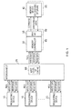
- FIG. 2 is a block diagram illustrating in more detail components provided within the memory controller 30 and the physical layer interface 35 in accordance with one embodiment.
- the memory controller 30 includes a protocol converter 100 for converting between the communication protocol used over the interconnect 25 and the protocol to be used for communicating with the memory device 40.
- a protocol converter 100 for converting between the communication protocol used over the interconnect 25 and the protocol to be used for communicating with the memory device 40.
- Each pending access request in the buffer will identify the address to be accessed, along with associated information such as the type of access to be performed.
- the write data can also be buffered in the pending access request buffer(s).
- a scheduler circuit 120 is used to perform scheduling operations in respect of the contents of the pending access request buffer(s) in order to determine the order in which to issue the pending access requests to the memory device. This can take into account the structure and organisation of the memory device in order to seek to optimise the performance of the memory accesses. For example, when a particular page is open in DRAM memory, it is typically more efficient to continue to access the contents of that page rather than closing the page and opening another page. Hence, pending access requests can be reordered by the scheduler with the aim of seeking to perform multiple accesses to an open page in the DRAM memory.
- Access execution circuitry 130 is used to issue selected access requests from the buffer 110 (as ordered by the scheduler 120) to the physical layer interface for onward propagation over the physical connection medium to the memory device 40.
- the physical layer interface 35 includes a command module 145 for issuing the command signal which will identify the type of access and the address being accessed, and a data module 140 for outputting write data to the memory device, or for receiving read data from the memory device.
- a synchronisation control component 150 controls the operation of the command module and the data module in order to maintain synchronous communication over the physical connection between the physical layer interface 35 and the memory device 40.
- the synchronisation control block will include a number of circuits such as phase-lock-loop circuits and delay-lock-loop circuits that are configured to seek to take account of delays, both relative and absolute, in the paths between the physical layer interface and the memory device.
- a clock signal is issued in association with the command signal from the command module to provide a timing reference
- a strobe signal is issued in association with the data signals to ensure that the data is latched on appropriate clock edges of the clock signal.
- Physical layer training circuitry 160 can be provided for performing such a training operation as and when required, and can apply a number of processes such as read/write levelling, data eye training, per-bit data deskew control, and PVT (process, voltage, temperature) compensation using any of a number of known techniques.
- the training circuitry 160 may be arranged to initiate the training operation periodically, for example on elapse of a predetermined time period, or may be arranged to actively monitor the quality of the signals being communicated over the connection with the memory device so as to seek to detect when such drifting issues are reaching a point where there is an unacceptable probability that an error may soon occur.
- the storage structures that are used to form the pending access requests buffer(s) 110 can take a variety of forms. However, in one embodiment at least the storage elements used to store the write data (and any read data that is temporarily buffered when being returned via the access execution circuitry to the protocol converter for onward propagation to the interconnect) comprise SRAM cells. In some embodiments, the remaining parts of the access request information, for example the address and access type information, can be stored in different storage structures such as flops, or alternatively such information may also be stored in SRAM cells if desired.
- a built-in self-test (BIST) controller 170 is provided for performing periodic checks on the SRAM cells in order to determine the presence of any hard errors, indicating faults in the operation of individual SRAM cells. It is typically the case that such BIST test procedures are performed at manufacture time, and optionally at boot time, but previously it has been not typically considered necessary to perform such tests during "live” operation of the memory controller.
- BIST test procedures are performed at manufacture time, and optionally at boot time, but previously it has been not typically considered necessary to perform such tests during "live” operation of the memory controller.
- certain emerging applications are becoming highly sensitive to errors, and in such applications it is advantageous to be able to perform such BIST testing periodically whilst the memory controller is being used, so that any faulty cells can be bypassed and no longer used (often a certain number of redundant cells can be provided that can be switched in in place of any such bypassed cells).
- a typical BIST testing operation may temporarily store the current data content from a series of memory cells into a buffer, and then perform one or more write and read sequences where known patterns are written to the cells and then read back from the cells in order to seek to detect situations where any of the cells are exhibiting a hard error. Assuming that test process is passed, then the data that has been temporarily buffered can be written back into the cells, and the BIST controller 170 can update its records to identify that that series of cells has passed the test.
- this potential impact is alleviated by arranging the BIST controller 170 to perform such BIST testing whilst a training operation is being performed in respect of the physical layer interface 35.
- the physical layer training circuitry 160 is arranged, when a training event occurs that causes the training circuitry to determine that a training operation should be initiated on the physical layer interface 35, to also issue a trigger to the BIST controller 170 to trigger performance of the BIST maintenance operation. This means that the BIST maintenance operation can be performed during a period of time when no active pending access requests can be processed anyway, and accordingly no such contention issues arise.
- the training circuit 160 may be a dedicated hardware circuit used to perform the training operation, by liaising with the synchronisation control block 150 in order to cause a series of test commands to be issued to the memory, with the various signals being monitored in order to determine how best to adjust the various synchronisation control parameters maintained within the synchronisation control block 150.
- the training circuitry may be provided with a dedicated connection via which it can issue the trigger signal directly to the BIST controller 170 as shown in Figure 2 .
- the training circuitry 160 may be implemented by a more general purpose processor executing firmware in order to perform the training operation.
- a processor may be connected via a peripheral bus with various components of the memory controller 30 and the physical layer interface 35 in order to not only perform the training operation in respect of the physical layer interface 35, but also to set values in certain control registers 180 of the memory controller to control the operation of the memory controller.
- one of the control registers 180 can be used to maintain a value which, when set to a predetermined value, triggers an interrupt that causes an exception routine to be performed in order to initiate the BIST maintenance operation by the BIST controller 170.
- the training circuitry 160 may update the relevant control register 180 in order to trigger performance of the BIST maintenance operation by the BIST controller 170.
- any other handshaking method could be used instead of the control register update approach.
- the BIST controller 170 has been triggered to perform the BIST maintenance operation in such a manner, there are a number of mechanisms that can be used to determine how long the BIST controller should continue to perform that maintenance operation for. If it can be guaranteed that the entire block of SRAM cells can be subjected to BIST maintenance during the period that the physical layer interface 35 is being subjected to the training operation, then it can merely perform the entire BIST testing process on all SRAM cells and then terminate. However, where there is potential for the BIST testing operation to last longer than the time taken to perform the training operation, then it may be appropriate to introduce measures to ensure that the BIST testing operation is performed in multiple stages, with each stage being performed so as to coincide with a training operation.
- the BIST controller may in one embodiment be provided with information about the expected length of time of the training operation. This could be provided directly by the training circuitry 160 in association with the trigger information, with the BIST controller then tailoring the number of SRAM cells that it subjects to the BIST test process accordingly.
- the BIST controller may have access to some stored information 190 providing information about the expected timings for different types of training events, and the training circuitry 160 may provide, in association with the trigger or update signal, information about the type of training to be performed by the current training operation. In particular, dependent on the nature of the training event that causes the training to be initiated, the type of training performed may differ, and the duration may hence differ.
- the BIST controller can again determine a suitable length of time that it has available for performing BIST testing, and choose the SRAM cells to be subjected to BIST testing accordingly.
- the BIST controller 170 can keep records of which SRAM cells have been tested, so that as each training operation takes place, it can perform testing on another block of SRAM cells so as, over time, to perform BIST testing on all of the SRAM cells.
- the BIST controller may be arranged to just perform BIST testing for a predetermined period of time.
- that predetermined period of time may be set so as to represent an expected shortest period of the training operation so as to ensure that any BIST testing is completed by the time the training operation completes, and hence the BIST testing will not impact on the efficiency of processing of the pending access requests when the system goes live again following the end of the training operation on the physical layer interface 35.
- the maintenance operation that is performed whilst the training operation is taking place is a BIST testing operation
- the maintenance operation can alternatively, or in addition, take other forms.
- the scheduler 120 may already be arranged to perform certain maintenance operations as a background task during live operation of the memory controller, in order to seek to improve the overall performance of the memory access operations. For example, it could seek to merge certain requests and can perform certain scheduling/reordering operations on the contents of the pending access requests buffer 110. Whilst these can be performed as a background activity during normal use, there is a limit as to how much of that type of maintenance can be performed before the maintenance itself begins to impact on the throughput of the access requests due to the contention it introduces in the read and write accesses to the SRAM cells.
- the trigger could also optionally be provided to the scheduler 120 (or indeed could be provided instead to the scheduler rather than to the BIST controller 170), to enable the scheduler to more aggressively perform such maintenance operations during the period when the training circuitry 160 is performing its training operation on the physical layer interface 35.
- the scheduler 120 could also have access to the training event type timings in the storage 190 in order to determine a suitable length of time during which to aggressively schedule such maintenance operations.
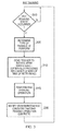
- Figure 3 is a flow diagram illustrating the operation of the training circuitry 160 in one embodiment.
- the training circuitry determines whether a physical layer ("phy") training event has occurred. As mentioned earlier, such a training event could occur due to the elapse of a timer, or due to the training circuit's monitoring of various signals issued through the physical layer interface 35 being indicative of an approaching error point being reached, for example due to drifting in the signals over the various physical wires.
- a physical layer (“phy) training event could occur due to the elapse of a timer, or due to the training circuit's monitoring of various signals issued through the physical layer interface 35 being indicative of an approaching error point being reached, for example due to drifting in the signals over the various physical wires.
- step 205 the type of training to be performed is determined.
- a trigger is then sent (optionally with associated timing information) to initiate SRAM maintenance in respect of the SRAM cells of the pending access requests buffer(s) 110, and then at step 215 the training operation is performed on the physical layer interface 35. Thereafter, the process may return to step 200, or optionally step 220 may be implemented where the training circuitry notifies the SRAM maintenance circuitry that the training operation is complete.
- That information could then be used by the maintenance circuitry (whether that be the BIST controller 170 or the scheduler 120) to terminate the ongoing maintenance operation, since once the training operation is complete, the memory controller 30 can return to live operation where the pending access requests can again begin to be processed for issuance to the memory device 40.
- FIG. 4 is a flow diagram illustrating the SRAM maintenance operation that may be performed in accordance with one embodiment. Whilst this process will be described with reference to the operation of the BIST controller 170, the same logical process can be applied by the scheduler 120 if it is arranged to respond to the trigger signal by performing certain maintenance operations.
- step 300 it is determined whether a trigger is received from the training circuitry, and once received, it is then determined at step 305 whether the length of the physical layer training operation is determinable. As mentioned earlier, this may be due to the training circuitry directly identifying the length of time that it is expecting to perform the training operation, or by the training circuitry identifying the type of training being performed, and the BIST controller having access to additional information to determine an expected length of time for such training. Assuming the length of time expected in relation to the training operation is determinable, then the process proceeds to step 310 where the maintenance circuitry refers to its record of previous maintenance in order to determine which SRAM cells (also referred to in Figure 4 as SRAM entries) to be subjected to SRAM maintenance.
- SRAM entries also referred to in Figure 4 as SRAM entries
- SRAM maintenance may be performed on a round-robin basis so that the least recently tested cells are the ones that are subjected to the current block of SRAM maintenance tasks. The number of SRAM cells to be subjected to SRAM maintenance during the current iteration will then be determined having regard to the timing information obtained at step 305.
- step 315 the SRAM maintenance is then performed for the selected SRAM cells, whereafter at step 320 the SRAM maintenance record is updated to identify that those cells have been subjected to the SRAM maintenance. The process then returns to step 300.
- step 305 If at step 305 it is determined that the length of time expected for the training operation is not determinable, then the process proceeds to step 325 where the record of previous maintenance is referred to in order to determine the first SRAM cell to be subjected to SRAM maintenance. Thereafter, at step 330 SRAM maintenance is performed on a series of SRAM cells starting with the first entry identified in step 325, either for a predetermined time period, or until the maintenance circuitry is notified that the training operation has completed. At that point, the process then proceeds to step 320 where the SRAM maintenance record is updated, and the process returns to step 300.
- the maintenance operation is performed in respect of the SRAM cells present within the pending access requests buffer(s) 110, such maintenance operations may additionally, or alternatively, be performed in respect of other storage structures within the system.
- the last level of cache 60 shown in Figure 1 may be relatively closely coupled with the memory controller, such that at least a significant portion of that cache is used to store information pertaining to pending access requests to the memory device 40.
- That cache may also consist of SRAM cells that would desirably be subjected to certain SRAM maintenance operations.
- the trigger signal issued by the training circuitry could if desired be issued to maintenance control circuitry for such a cache 60, in order to initiate performance of maintenance tasks in respect of the cache during the period in which the training operation is being performed on the physical layer interface 35.
- FIG. 5 is a flow diagram illustrating the operation of the scheduler 120 in one embodiment, and in particular the scheduler's operation in respect of maintenance operations, in an embodiment where the scheduler performs certain maintenance operations as a background task, but can be configured to be responsive to the trigger signal from the training circuitry to accelerate performance of those maintenance operations.
- step 350 it is determined whether a trigger has been received from the training circuitry 160. If not, then as indicated by step 355, the scheduler continues to perform background maintenance tasks at the same time as access requests are actively being processed by the memory controller. These background maintenance tasks may include certain scheduling/ordering tasks and/or request merging tasks as discussed earlier.
- the scheduler will typically perform arbitration amongst the pending access requests in the buffer in order to decide which access requests the access execution circuitry 130 issues via the physical layer interface 35 to the memory device 40. This process continues until receipt of the trigger signal is detected at step 350.
- processing instead branches to the lefthand side of the flow shown in Figure 5 .
- the arbitration process is halted, since no pending access requests will be issued whilst the physical layer training operation is taking place.
- the scheduler then employs aggressive maintenance, where the maintenance tasks that would typically be performed as background maintenance tasks are performed at an accelerated rate, taking advantage of there being no contention for SRAM bandwidth due to normal read/write activity. In particular, that normal read/write activity is not currently taking place due to no memory accesses being processed by the memory controller at the current time.
- step 370 The halting of the arbitration process, and the performance of aggressive maintenance, continues until it is determined at step 370 that the training operation in respect of the physical layer interface 35 has ended, at which point the process returns to step 350. At this point, no trigger will have been received, and the process will then proceed to step 355 where the normal operation of the scheduler is resumed.
- such embodiments provide an improved mechanism for handling maintenance operations in respect of storage elements associated with a memory controller, by concentrating the performance of those maintenance operations into periods of time where system transactions already need to be stalled, due to the requirement to perform a training operation in respect of the physical layer interface.
- the downtime introduced by the performance of the physical layer interface training is taken advantage of to also during that period perform certain maintenance operations on the storage elements, hence preventing the performance of those maintenance operations having any additional adverse effect on the memory access performance of the system.
- the maintenance circuitry can be configured to perform partial maintenance so as to only test certain parts of the SRAM memory array during each physical layer training process, so that over a number of iterations of the training operation the entire SRAM array can be tested.
- the words “configured to" are used to mean that an element of an apparatus has a configuration able to carry out the defined operation.
- a “configuration” means an arrangement or manner of interconnection of hardware or software.
- the apparatus may have dedicated hardware which provides the defined operation, or a processor or other processing device may be programmed to perform the function.
- Configured to does not imply that the apparatus element needs to be changed in any way in order to provide the defined operation.
Landscapes
- Engineering & Computer Science (AREA)
- Theoretical Computer Science (AREA)
- Physics & Mathematics (AREA)
- General Engineering & Computer Science (AREA)
- General Physics & Mathematics (AREA)
- Quality & Reliability (AREA)
- Computing Systems (AREA)
- Mathematical Physics (AREA)
- Computer Hardware Design (AREA)
- Human Computer Interaction (AREA)
- Debugging And Monitoring (AREA)
- Techniques For Improving Reliability Of Storages (AREA)
- Memory System (AREA)
- For Increasing The Reliability Of Semiconductor Memories (AREA)
Priority Applications (4)
| Application Number | Priority Date | Filing Date | Title |
|---|---|---|---|
| EP16176680.3A EP3264276A1 (de) | 2016-06-28 | 2016-06-28 | Vorrichtung zur steuerung des zugangs zu einer speichervorrichtung und verfahren zur durchführung von wartungsarbeiten in solch einer vorrichtung |
| US15/593,560 US10540248B2 (en) | 2016-06-28 | 2017-05-12 | Apparatus for controlling access to a memory device, and a method of performing a maintenance operation within such an apparatus |
| JP2017115652A JP2018005902A (ja) | 2016-06-28 | 2017-06-13 | メモリ装置へのアクセスを制御するための装置及びそのような装置内においてメンテナンス作業を行う方法 |
| CN201710475609.8A CN107544923B (zh) | 2016-06-28 | 2017-06-21 | 用于控制对存储器设备的访问的装置以及相关方法 |
Applications Claiming Priority (1)
| Application Number | Priority Date | Filing Date | Title |
|---|---|---|---|
| EP16176680.3A EP3264276A1 (de) | 2016-06-28 | 2016-06-28 | Vorrichtung zur steuerung des zugangs zu einer speichervorrichtung und verfahren zur durchführung von wartungsarbeiten in solch einer vorrichtung |
Publications (1)
| Publication Number | Publication Date |
|---|---|
| EP3264276A1 true EP3264276A1 (de) | 2018-01-03 |
Family
ID=56296561
Family Applications (1)
| Application Number | Title | Priority Date | Filing Date |
|---|---|---|---|
| EP16176680.3A Withdrawn EP3264276A1 (de) | 2016-06-28 | 2016-06-28 | Vorrichtung zur steuerung des zugangs zu einer speichervorrichtung und verfahren zur durchführung von wartungsarbeiten in solch einer vorrichtung |
Country Status (4)
| Country | Link |
|---|---|
| US (1) | US10540248B2 (de) |
| EP (1) | EP3264276A1 (de) |
| JP (1) | JP2018005902A (de) |
| CN (1) | CN107544923B (de) |
Families Citing this family (13)
| Publication number | Priority date | Publication date | Assignee | Title |
|---|---|---|---|---|
| US10339050B2 (en) * | 2016-09-23 | 2019-07-02 | Arm Limited | Apparatus including a memory controller for controlling direct data transfer between first and second memory modules using direct transfer commands |
| US10347357B2 (en) * | 2017-04-24 | 2019-07-09 | Intel Corporation | Post-packaging environment recovery of graphics on-die memory |
| WO2019169615A1 (zh) * | 2018-03-09 | 2019-09-12 | 深圳市汇顶科技股份有限公司 | 访问指令sram的方法和电子设备 |
| CN110618903B (zh) * | 2018-06-19 | 2024-12-10 | 北京忆恒创源科技股份有限公司 | 电子设备测试方法与装置 |
| JP2020047340A (ja) | 2018-09-19 | 2020-03-26 | キオクシア株式会社 | 不揮発性メモリ及びメモリシステム |
| KR102728324B1 (ko) | 2019-12-03 | 2024-11-08 | 에스케이하이닉스 주식회사 | 메모리 시스템 및 메모리 시스템의 트레이닝 방법 |
| KR102804852B1 (ko) * | 2019-12-23 | 2025-05-09 | 주식회사 엘엑스세미콘 | 메모리 컨트롤러, 및 이의 동작 방법 |
| KR102804862B1 (ko) * | 2019-12-23 | 2025-05-09 | 주식회사 엘엑스세미콘 | 메모리 컨트롤러, 및 이의 동작 방법 |
| US12197766B2 (en) * | 2020-11-10 | 2025-01-14 | Micron Technology, Inc. | Error injection methods using soft post-package repair (sPPR) techniques and memory devices and memory systems employing the same |
| TWI811606B (zh) * | 2020-12-31 | 2023-08-11 | 新唐科技股份有限公司 | 事件觸發主控端、控制晶片及控制方法 |
| US12444476B2 (en) * | 2022-03-14 | 2025-10-14 | Micron Technology, Inc. | Host controlled media testing of memory |
| CN115344215B (zh) * | 2022-08-29 | 2025-03-18 | 深圳市紫光同创电子股份有限公司 | 存储器训练方法及系统 |
| US12608654B2 (en) * | 2024-01-09 | 2026-04-21 | Qualcomm Incorporated | Memory device high-speed interface training |
Citations (3)
| Publication number | Priority date | Publication date | Assignee | Title |
|---|---|---|---|---|
| US20130227183A1 (en) * | 2010-11-09 | 2013-08-29 | Rambus Inc. | Memory access during memory calibration |
| US20140281161A1 (en) * | 2013-03-14 | 2014-09-18 | Micron Technology, Inc. | Memory systems and methods including training, data organizing, and/or shadowing |
| US20160064066A1 (en) * | 2009-01-22 | 2016-03-03 | Rambus Inc. | Maintenance operations in a dram |
Family Cites Families (12)
| Publication number | Priority date | Publication date | Assignee | Title |
|---|---|---|---|---|
| WO1999046775A2 (en) * | 1998-03-10 | 1999-09-16 | Rambus, Inc. | Performing concurrent refresh and current control operations in a memory subsystem |
| US6631440B2 (en) * | 2000-11-30 | 2003-10-07 | Hewlett-Packard Development Company | Method and apparatus for scheduling memory calibrations based on transactions |
| US20070250283A1 (en) * | 2006-04-25 | 2007-10-25 | Barnum Melissa A | Maintenance and Calibration Operations for Memories |
| JP2008269669A (ja) * | 2007-04-17 | 2008-11-06 | Renesas Technology Corp | 半導体装置及びデータ処理システム |
| GB2451668A (en) * | 2007-08-08 | 2009-02-11 | Advanced Risc Mach Ltd | Error correction in a set associative cache |
| US9176859B2 (en) * | 2009-01-07 | 2015-11-03 | Siliconsystems, Inc. | Systems and methods for improving the performance of non-volatile memory operations |
| US8127087B2 (en) * | 2009-02-12 | 2012-02-28 | International Business Machines Corporation | Memory controller for improved read port selection in a memory mirrored system |
| US8230260B2 (en) * | 2010-05-11 | 2012-07-24 | Hewlett-Packard Development Company, L.P. | Method and system for performing parallel computer tasks |
| US9432298B1 (en) * | 2011-12-09 | 2016-08-30 | P4tents1, LLC | System, method, and computer program product for improving memory systems |
| US9632954B2 (en) * | 2011-11-07 | 2017-04-25 | International Business Machines Corporation | Memory queue handling techniques for reducing impact of high-latency memory operations |
| US9639495B2 (en) * | 2014-06-27 | 2017-05-02 | Advanced Micro Devices, Inc. | Integrated controller for training memory physical layer interface |
| US20160239442A1 (en) * | 2015-02-13 | 2016-08-18 | Qualcomm Incorporated | Scheduling volatile memory maintenance events in a multi-processor system |
-
2016
- 2016-06-28 EP EP16176680.3A patent/EP3264276A1/de not_active Withdrawn
-
2017
- 2017-05-12 US US15/593,560 patent/US10540248B2/en active Active
- 2017-06-13 JP JP2017115652A patent/JP2018005902A/ja active Pending
- 2017-06-21 CN CN201710475609.8A patent/CN107544923B/zh active Active
Patent Citations (3)
| Publication number | Priority date | Publication date | Assignee | Title |
|---|---|---|---|---|
| US20160064066A1 (en) * | 2009-01-22 | 2016-03-03 | Rambus Inc. | Maintenance operations in a dram |
| US20130227183A1 (en) * | 2010-11-09 | 2013-08-29 | Rambus Inc. | Memory access during memory calibration |
| US20140281161A1 (en) * | 2013-03-14 | 2014-09-18 | Micron Technology, Inc. | Memory systems and methods including training, data organizing, and/or shadowing |
Also Published As
| Publication number | Publication date |
|---|---|
| US10540248B2 (en) | 2020-01-21 |
| US20170371560A1 (en) | 2017-12-28 |
| JP2018005902A (ja) | 2018-01-11 |
| CN107544923B (zh) | 2023-09-01 |
| CN107544923A (zh) | 2018-01-05 |
Similar Documents
| Publication | Publication Date | Title |
|---|---|---|
| US10540248B2 (en) | Apparatus for controlling access to a memory device, and a method of performing a maintenance operation within such an apparatus | |
| EP3270290B1 (de) | Ddr-speicherfehlerkorrektur | |
| KR100813422B1 (ko) | 메모리 허브 및 메모리 시퀀싱 방법 | |
| US7979759B2 (en) | Test and bring-up of an enhanced cascade interconnect memory system | |
| US8880833B2 (en) | System and method for read synchronization of memory modules | |
| US10042700B2 (en) | Integral post package repair | |
| JP6535517B2 (ja) | データ処理装置用のメモリ・ビルトイン・セルフテスト | |
| TWI428757B (zh) | 記憶體之快速資料眼再訓練之方法、裝置及系統 | |
| US20060206761A1 (en) | System and method for on-board timing margin testing of memory modules | |
| CN114902198B (zh) | 用于异构存储器系统的信令 | |
| JP2016520226A (ja) | 領域特有のメモリアクセススケジューリングを有するメモリシステム | |
| JP2024512625A (ja) | アービトレーション中の書き込みバンクグループのマスク | |
| KR20220116033A (ko) | 비휘발성 메모리 모듈에 대한 오류 복구 | |
| EP3249533A1 (de) | Integrierte postverpackungsreparatur |
Legal Events
| Date | Code | Title | Description |
|---|---|---|---|
| PUAI | Public reference made under article 153(3) epc to a published international application that has entered the european phase |
Free format text: ORIGINAL CODE: 0009012 |
|
| STAA | Information on the status of an ep patent application or granted ep patent |
Free format text: STATUS: THE APPLICATION HAS BEEN PUBLISHED |
|
| AK | Designated contracting states |
Kind code of ref document: A1 Designated state(s): AL AT BE BG CH CY CZ DE DK EE ES FI FR GB GR HR HU IE IS IT LI LT LU LV MC MK MT NL NO PL PT RO RS SE SI SK SM TR |
|
| AX | Request for extension of the european patent |
Extension state: BA ME |
|
| STAA | Information on the status of an ep patent application or granted ep patent |
Free format text: STATUS: REQUEST FOR EXAMINATION WAS MADE |
|
| 17P | Request for examination filed |
Effective date: 20180703 |
|
| RBV | Designated contracting states (corrected) |
Designated state(s): AL AT BE BG CH CY CZ DE DK EE ES FI FR GB GR HR HU IE IS IT LI LT LU LV MC MK MT NL NO PL PT RO RS SE SI SK SM TR |
|
| STAA | Information on the status of an ep patent application or granted ep patent |
Free format text: STATUS: THE APPLICATION HAS BEEN WITHDRAWN |
|
| 18W | Application withdrawn |
Effective date: 20180809 |