EP3267184B1 - Procédé et système pour déterminer la position d'une source de rayonnement - Google Patents
Procédé et système pour déterminer la position d'une source de rayonnement Download PDFInfo
- Publication number
- EP3267184B1 EP3267184B1 EP16178468.1A EP16178468A EP3267184B1 EP 3267184 B1 EP3267184 B1 EP 3267184B1 EP 16178468 A EP16178468 A EP 16178468A EP 3267184 B1 EP3267184 B1 EP 3267184B1
- Authority
- EP
- European Patent Office
- Prior art keywords
- detector
- pixels
- pixel
- radiation
- orientation
- Prior art date
- Legal status (The legal status is an assumption and is not a legal conclusion. Google has not performed a legal analysis and makes no representation as to the accuracy of the status listed.)
- Active
Links
Images


Classifications
-
- G—PHYSICS
- G01—MEASURING; TESTING
- G01B—MEASURING LENGTH, THICKNESS OR SIMILAR LINEAR DIMENSIONS; MEASURING ANGLES; MEASURING AREAS; MEASURING IRREGULARITIES OF SURFACES OR CONTOURS
- G01B15/00—Measuring arrangements characterised by the use of electromagnetic waves or particle radiation, e.g. by the use of microwaves, X-rays, gamma rays or electrons
-
- G—PHYSICS
- G01—MEASURING; TESTING
- G01N—INVESTIGATING OR ANALYSING MATERIALS BY DETERMINING THEIR CHEMICAL OR PHYSICAL PROPERTIES
- G01N23/00—Investigating or analysing materials by the use of wave or particle radiation, e.g. X-rays or neutrons, not covered by groups G01N3/00 – G01N17/00, G01N21/00 or G01N22/00
- G01N23/20—Investigating or analysing materials by the use of wave or particle radiation, e.g. X-rays or neutrons, not covered by groups G01N3/00 – G01N17/00, G01N21/00 or G01N22/00 by using diffraction of the radiation by the materials, e.g. for investigating crystal structure; by using scattering of the radiation by the materials, e.g. for investigating non-crystalline materials; by using reflection of the radiation by the materials
- G01N23/203—Measuring back scattering
-
- G—PHYSICS
- G01—MEASURING; TESTING
- G01T—MEASUREMENT OF NUCLEAR OR X-RADIATION
- G01T1/00—Measuring X-radiation, gamma radiation, corpuscular radiation, or cosmic radiation
- G01T1/29—Measurement performed on radiation beams, e.g. position or section of the beam; Measurement of spatial distribution of radiation
- G01T1/2907—Angle determination; Directional detectors; Telescopes
-
- G—PHYSICS
- G01—MEASURING; TESTING
- G01N—INVESTIGATING OR ANALYSING MATERIALS BY DETERMINING THEIR CHEMICAL OR PHYSICAL PROPERTIES
- G01N2223/00—Investigating materials by wave or particle radiation
- G01N2223/50—Detectors
- G01N2223/501—Detectors array
Definitions
- the present invention relates to a method and a system for determining the position of a radiation source, particularly for use in crystallographic applications.
- the invention further relates to the use of a pixel detector for determining the position of a radiation source, a computer readable medium related thereto and a sample for a system according to the present invention.
- Maurice et al. disclosed a moving screen method for accurate localization of the pattern center of diffraction patterns in EBSD.
- two diffraction patterns are obtained with two relative positions of detector screen and sample and are thus optically zoomed relative to each other.
- One of the patterns is then virtually zoomed, i.e. the projection center coordinates are varied, until the cross-correlation with the other pattern reaches a maximum.
- a shift value for determining the pattern center relative to the image center can be obtained ( C. Maurice, K. Dzieciol, R. Fortunier, Ultramicroscopy, 111,140 (2011 )).
- US 3,581,090 B discloses a system for deriving the position of a radiation source, wherein the system comprises a stationary array of at least three receivers for said radiation and at least three shield means disposed between each of the radiators and the radiation source.
- the shield means cast shadows on the respective detectors, wherein the shadowed detector portion depends on the position of the radiation source relative to shield mean and detector. From the intensities detected by the individual detectors the position of the radiation source can be derived.
- the system requires an array of multiple detectors and shield means and is not suitable for being integrated in a structure analysis apparatus.
- periodic structure herein denotes a structure that is spatially repeating with a repeat unit in the order of the wavelength of the radiation emitted from the localized radiation source.
- the periodic structure is a three-dimensional periodic structure.
- the method according to the invention is based on the finding, that due to the fixed internal periodic structure of the pixels, the detector comprises a sensitivity in detecting incident radiation of wavelength ⁇ that depends on the incidence direction of the radiation on each area element dA and thus on each pixel of the detector.
- the position of a radiation source is determined in the present invention, it is the wave character of the radiation emitted by that source that allows to determine the incident direction of the radiation.
- a predetermined intensity distribution i.e. a known distribution or a reliably estimated distribution
- irradiated on the pixel detector produces a detected intensity pattern, i.e. an intensity value for each of the plurality of pixels, that is not a homogenous transformation of the incident intensity for all of the pixels, but is additionally modulated based on the incidence direction and on the wavelength of the incident radiation.
- a detected intensity pattern i.e. an intensity value for each of the plurality of pixels, that is not a homogenous transformation of the incident intensity for all of the pixels, but is additionally modulated based on the incidence direction and on the wavelength of the incident radiation.
- the information on an orientation of a periodic structure at each of the pixels preferably refer to information on the type of periodic structure, on characteristic distances of that structure and/or on the orientation of that structure relative to a sensor surface of the pixel detector, i.e. a surface formed by a plurality of the pixels.
- the periodic internal structure is a crystal structure
- the information on an orientation of a periodic structure preferably refer to information on the type of crystal lattice, the lattice constant(s) of this crystal lattice and/or the orientation of the lattice relative to a sensor surface of the pixel detector, e.g. in form of a set of Euler angles.
- standing waves will have maxima on the lattice planes or between them.
- the multiple Bragg-reflections causes standing waves with maxima between the atomic planes, the backscattering will be reduced, and the incident electrons can penetrate deeper into the crystal.
- the density of scattering centers experienced by the electron differs with the angle of the electron relative to the crystal lattice planes, e.g. this is characteristically varying for an electron beam with an incidence direction that is near the Bragg angle of a crystal lattice plane.
- the detected intensity pattern shows features that are basically related to the Bragg angles for the lattice planes of the periodic structure, e.g. crystalline structure, of the detector.
- a detailed discussion of the physical effects underlying electron channeling and detector channeling as well as mathematical relationships that can be used to determine the incidence direction using information on an crystal orientation of a periodic structure, preferably a crystal orientation, at the pixel and on the predetermined intensity distribution at the pixel, wavelength ⁇ and the detected intensity at the pixel can be found in D.C.Joy et al. J.Appl.Phys. 53 R 81 (1982 ). It is further referred to V.I. Vysotski et al. Channeling of neutral particles and photons in crystals Soviet Physics Uspheki Vol. 35, No. 9, (1992 ) addressing the effect of channeling of neutral particles, e.g. neutrons, and photons, e.g., X-ray, in a homogeneous lattice.
- a pixel detector comprising a periodic structure, preferably a crystalline material, with (lattice) planes that are tilted with respect to the detector surface
- the incident intensity is modulated in dependence of both a polar component ⁇ i and an azimuthal component ⁇ i of an angle of incidence of the incident radiation.
- the modulated detected intensity distribution, the wavelength ⁇ and the orientation of the periodic structure, preferably the crystal orientation, for each pixel of the plurality of pixels, respectively it is possible to determine the polar component ⁇ i and/or an azimuth component ⁇ i of an angle of incidence of the incident radiation.
- the calibration procedure preferably involves the quantitative comparison of at least one, preferably multiple, detected intensity patterns (DCP) with theoretical simulations of a detected intensity pattern, wherein the simulations depend on assumed radiation source positions and assumed internal orientations of a periodic structure, e.g. an internal orientation of a crystal structure with respect to the detector surface.
- DCP detected intensity patterns
- the simulations are preferably conducted using a many-beam dynamical simulation based on the Bloch wave theory of electron diffraction.
- a further definition of the theory underlying a suitable simulation and mathematical description of such simulation can be found in A. Winkelmann et al. Ultramicroscopy 107, 414 (2007 ).
- the assumed orientation of the periodic structure within each of the plurality of pixels preferably corresponds to manufacturer specifications of the orientation of a crystalline detector material.
- the assumed crystal orientation is based on this manufacturer specification.
- the simulations for the detected intensity patterns are solely based on the assumption of a fixed but unknown orientation of the internal periodic structure of the detector, particularly for single-crystalline detector volumes. The so produced simulations for detected intensity patterns are compared to the detected intensity patterns obtained in the calibration process and are varied until the cross-correlation coefficient between measured and simulated patterns reaches a maximum.
- the calibration procedure is skipped in the method according to the present invention and the information on the orientation of the periodic structure for each of the plurality of pixels is provided by the manufacturer or is determined in an individual measurement.
- the fixed orientation of the periodic internal structure, e.g the crystal orientation, of the detector pixels can be independently determined by X-ray diffraction using a suitable goniometer. In principle any measurement technique providing accurate information on this orientation can be used.
- the orientation of the periodic structure within the detector pixels is fixed for the lifetime of the detector it is the same for all subsequent experiments using this detector.
- the information on the periodic structure provided by the manufacturer or determined in an independent measurement is used as determined orientation of the periodic structure in following measurements and determinations of the incidence direction.
- the orientation of the periodic structure that was determined in the calibration is used in following simulations for detected intensity patterns in order to determine that radiation source position according to the method of the present invention.
- the radiation source position is varied until in the comparison of the simulated and obtained detected intensity patterns yields a maximum cross-correlation coefficient. From the simulated pattern of the detected intensities that fits best to the actual detected intensity pattern, the radiation source position is obtained.
- the optimization of a cross-correlation coefficient can be exchanged with another image fitting algorithm that achieves similar results, i.e. that is capable of optimizing a numerical value for the similarity of two images.
- the incident intensity distribution is equal for each of the plurality of pixels. Consequently, each modulation of, or each contrast in, the detected intensity pattern is solely provided by detector channeling as described above.
- the information that the predetermined intensity distribution is isotropic, i.e. equal for each of the plurality of pixels, is sufficient in determining the incidence direction for the incident direction, i.e. for the simulations as described above.
- the predetermined intensity distribution incident on the detector surface is non-isotropic.
- the information on the predetermined intensity distribution must be more detailed and must at least contain contrast information for the incident intensity pattern on the detector surface due to the predetermined intensity distribution.
- at least the relative incident intensities of the plurality of pixels i.e. the ratio of incident intensities of two of the plurality of pixels at a time, must be known.
- orientations of the internal periodic structure of different pixels must be then considered in the simulations of detected intensity patterns for the calibration procedure as described above.
- orientations of several internal periodic structures i.e. orientation of several crystal structures relative to the detector surface, are determined either for individual pixels or for groups of pixels.
- the several determined orientations of periodic structures are then set as orientations for the respective pixels.
- the sample region comprises a polycrystalline or amorphous material that is configured for quasi-isotropically reflecting or deflecting the primary radiation.
- the secondary radiation constituting the predetermined intensity distribution irradiating the detector surface is thus a quasi-isotropic intensity distribution in this embodiment.
- the sample region comprises a crystalline or polycrystalline material that is configured for anisotropically reflecting or deflecting the primary radiation.
- the secondary radiation then constitutes an anisotropic predetermined intensity distribution irradiating the detector surface.
- the computer-readable medium comprises program instructions, wherein when executed in a control unit of a system as described above the program instructions are operable to perform a method as described above.
- Another aspect of the present invention relates to the use of a pixel detector for determining a position of a divergent radiation source according to the appended claims.
- a pixel detector for determining a position of a divergent radiation source according to the appended claims.
- the advantages as described with respect to the method according to the present invention can be achieved with any apparatus, e.g. a structure analysis apparatus, comprising a divergent radiation source and a suitable pixel detector.
- the determined position is used to determine a three dimensional pattern from its two dimensional projection onto the pixel detector, i.e. onto the detector surface of the pixel detector that is formed by a plurality of pixels.
- FIG. 1 an exemplary embodiment of a system according to the invention is shown, the system being integrated in a scanning electron microscope (SEM) as an apparatus for electron backscatter diffraction.
- SEM scanning electron microscope
- the SEM comprises an electron source 7 as primary radiation source that radiates a sample 8 with a focused electron beam 9 as primary radiation.
- the electron beam 9 is focused on a region of a sample 8 and is diffracted by the sample in this region. Thereby, the sample region becomes a divergent radiation source 1 for backscattered electrons 10 that are incident on a detector surface 4 of sensor 3.
- Figure 2 (A) shows a schematic illustration of the detector channeling effect that is the physical effect underlying the method according to the invention.
- the latter effect results e.g. if backscattered electrons 10, as shown in Fig. 1 , are irradiated on a detector surface 4, as shown in Fig. 1 , comprising a crystalline structure with multiple crystal lattice planes 11.
- the electrons 10 emitted from the radiation source 1 travel towards the detector plane 4 that is made from a silicon wafer cut in (111) orientation.
- the electrons impinge on each pixel 4a of detector surface 4 at a specific incidence direction, e.g. given by the polar component ⁇ i of the angle of incidence of the incident radiation with respect to the surface normal of the detector surface 4 and the azimuth component ⁇ i of the angle of incidence of the incident radiation with respect to the surface plane of the detector surface 4.
- the penetration depth of the incident radiation 10 into the silicon detector volume 5 is determined by multiple electron reflections at the silicon crystal lattice planes 11 within the detector volume 5 and changes near the Bragg angle, because of the preferential excitation of Bloch waves that are localized either on lattice planes or exactly between them (cf. D.C.Joy et al. J.Appl.Phys. 53 R 81 (1982 )). Since the incident radiation 10 penetrates to various depths into the detector volume 5, the excitation of electron-hole pairs in the silicon voxel, i.e. the intensity detected at this pixel, is changed as a function of the incidence direction, as shown in Fig. 2 . Because the electrons can go less deep when there is a large backscattered signal, the detected intensity pattern modulated by the detector channeling effect is negatively proportional to the backscattered intensity as shown in Fig. 2 (B) .
- the detector channeling effect thus provides a one-to-one relationship between pixel position (x i , y i ) on detector surface 4 and the incidence direction of the incident radiation and thus the radiation source position (x SOURCE , y SOURCE , z SOURCE ).
- planar detector surface 4 with area elements dA n is reacting to diffraction effects of incident radiation from the source 1 in the area element dA n .
- Each area element dA n at a specific position (x n , y n ) on the detector is showing an intensity which is related to the direction from the radiation source 1 to the area element dA n and vice versa.
- a triangulation procedure involving the intensities from all area elements dA n ; i.e. from all pixels, of the detector 2 thus allows to pinpoint the position of source 1.
- FIG. 4 An exemplary detected intensity pattern solely modulated by the detector channeling effect, i.e. a pure detector diffraction pattern, is shown in Fig. 4 .
- the shown 2D intensity pattern is visible in the detector response even in total absence of diffraction effects from sample 8.
- the observed patterns further have the negative intensity distribution relative to what is usually observed for backscattered electrons from a crystal.
- these patterns are interpreted as electron channeling patterns formed not by the sample 8 but in the crystalline detector volume 5 instead.
- a pattern as shown in Fig. 4 will be obtained by detecting an incident radiation from an amorphous sample 8 as divergent radiation source 1 of deflected or reflected primary radiation with a single-crystalline detector made from a silicon wafer cut in (111) orientation.
- the detector channeling pattern gives crystal lattice directions ("zone axes") as crossing points of the center lines of the Kikuchi bands seen in the pattern.
- the angles between all lattice directions are known for the detector structure used and thus provide the calibration reference values.
- one can (a) determine the two-dimensional position (x i , y i ) of the crossing points (zone axes) in the measured pattern image and (b) assign the respective three-dimensional lattice direction [u i v i w i ] to each of these points.
- the remaining z-component Z SOURCE of the source point can be obtained by calculating right-angled triangle(s), with the 90° angle between the experimentally measured 2D vector(s) (x i - x N , y i , - y N ) and the surface normal.
- the 2D vector(s) (x i - x N , y i , - y N ) in the detector plane subtend the known angle(s) ⁇ i between [u i v i w i ] and [u N v N w N ] as viewed from the source point.
- , i.e. Z SOURCE d i /tan( ⁇ i ).
- the accuracy of the Z SOURCE value depends on the method used to identify the corresponding (x i , y i ) and (x N , y N ) in the pattern image.
- the precision of the method can be estimated from the statistical variation of the values of Z SOURCE in dependence on the various measured d i .
- the complete information present in the pattern i.e.
- FIG. 5 shows a calibration of the inverted detected intensity pattern (left side) solely modulated by the detector channeling effect by comparison with a simulation for a detected intensity pattern (right side) that was produced using the dynamical theory of electron diffraction (cf. A. Winkelmann et al. Ultramicroscopy 107, 414 (2007 )).
- the 3D parameters of the electron source (X SOURCE , Y SOURCE , Z SOURCE ) and the internal orientation of the silicon crystal structure with respect to the detector surface plane are input to the simulation and a best-fit optimization procedure gives the 3D parameters of the electron source (X SOURCE , Y SOURCE , Z SOURCE ).
- the internal orientation of the silicon crystal structure relative to the edges of the detector is be described by Euler angles ( ⁇ 1 , ⁇ , ⁇ 2 ) that describe a rotation sequence around moving ZXZ-axes in the Bunge convention.
- the fixed detector crystal orientation is estimated as the mean orientation determined from a series of measurements which consist in moving the 12 keV electron beam 9 in a regular two-dimensional grid over the surface of a sample 8 that shows no backscattering diffraction pattern.
- the calibration procedure for each measured pattern involves the quantitative comparison of the measured pattern with theoretical simulations depending on the radiation source 1 position and the internal orientation of the silicon crystal structure with respect to the detector surface 4.
- the best fit orientation was determined by the optimization of the normalized cross-correlation coefficient r relative to simulated Kikuchi data for silicon.
- the software ESPRIT DynamicS by Bruker Nano, Berlin, was applied.
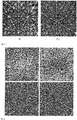
- Fig. 6 shows a Kikuchi pattern measurement at 25 keV using a silicon sample covered by 10 nm of nanocrystalline HfO 2 , which for Kikuchi pattern formation can be considered amorphous.
- the crystal orientation in the detector volume 5 was assumed at the values of (179.95, 54.53, 45.15) as determined above.
- the panels in the top row of Fig. 6 show the measured pattern (left) and an inverted copy (right) of that pattern.
- the lower panel shows on the right side the best-fit simulation for the radiation source 1 position from the negative of the total experimental pattern.
- the radiation source 1 position i.e.
- the pixel detector used in the method according to the embodiment described above comprises a sensor 3 with a detector surface 4, divided into a plurality of pixels 4a with pixel coordinates (xi, yi, zi), and a detector volume 5, divided into a plurality of voxels 5a corresponding to the plurality of pixels 4a.
- Each voxel 5a comprises a crystalline material with fixed crystal orientation.
- the pixel detector further comprises an electronics chip 6 with a plurality of amplification pixels 6a, each corresponding to one of the plurality of pixels 4a.
Landscapes
- Physics & Mathematics (AREA)
- General Physics & Mathematics (AREA)
- Chemical & Material Sciences (AREA)
- Life Sciences & Earth Sciences (AREA)
- Health & Medical Sciences (AREA)
- Analytical Chemistry (AREA)
- Biochemistry (AREA)
- General Health & Medical Sciences (AREA)
- Crystallography & Structural Chemistry (AREA)
- Immunology (AREA)
- Pathology (AREA)
- High Energy & Nuclear Physics (AREA)
- Molecular Biology (AREA)
- Spectroscopy & Molecular Physics (AREA)
- Electromagnetism (AREA)
- Analysing Materials By The Use Of Radiation (AREA)
Claims (14)
- Procédé pour déterminer une position d'une source de rayonnement divergent (1), comprenant :irradier un détecteur de pixels (2) avec une répartition d'intensité prédéterminée du rayonnement incident (10) avec une longueur d'onde λ issue de la source de rayonnement divergent (1), le rayonnement incident (10) étant des électrons, des neutrons ou des rayons X, et le détecteur de pixels (2) comprenant une pluralité de pixels (4a) avec les coordonnées de pixels (xi, yi; zi), chaque pixel (4a) ayant une structure périodique interne qui est répétée spatialement avec une unité de répétition dans l'ordre de la longueur d'onde λ ;détecter un motif de canalisation de détecteur, DCP, comprenant, pour chaque pixel de la pluralité de pixels (4a), une intensité détectée de rayonnement incident (10) ;déterminer, pour chaque pixel de la pluralité de pixels (4a), une direction d'incidence du rayonnement incident (10) en utilisant des informations sur une orientation de la structure périodique interne au sein du pixel (4a), sur la répartition d'intensité prédéterminée, sur la longueur d'onde λ et sur l'intensité détectée du rayonnement incident (10) ; etdéterminer la position (xp, yp, zp) de la source de rayonnement divergent (1) en utilisant les coordonnées de pixel (xi, yi, zi) et la direction d'incidence pour chaque pixel de la pluralité de pixels (4a).
- Procédé selon la revendication 1, comprenant en outre :
déterminer, pour chaque pixel de la pluralité de pixels (4a), une composante polaire ϕi, et/ou une composante azimutale θi d'un angle d'incidence du rayonnement incident (10) en utilisant des informations sur l'orientation de la structure périodique interne au sein du pixel (4a), sur la répartition d'intensité prédéterminée, sur la longueur d'onde λ et sur l'intensité détectée du rayonnement incident (10). - Procédé selon l'une quelconque des revendications précédentes, comprenant en outre :
déterminer, pour chaque pixel de la pluralité de pixels (4a), l'orientation de la structure périodique interne au sein du pixel (4a), en :comparant l'intensité détectée du rayonnement incident (10) avec une intensité simulée, l'intensité simulée étant fonction d'une orientation présumée de la structure périodique interne et d'une position présumée de la source de rayonnement divergent (1) ou de la mesure de l'orientation de la structure périodique interne à l'aide d'une mesure indépendante ;déterminer, pour chaque pixel de la pluralité de pixels (4a), une direction d'incidence et la position (xp, yp, zp) de la source de rayonnement divergent (1), en :
comparant l'intensité détectée du rayonnement incident (10) avec une intensité simulée, l'intensité simulée étant fonction de l'orientation déterminée de la structure périodique interne et d'une position présumée de la source de rayonnement divergent (1). - Procédé selon la revendication 3, caractérisé en ce que :
l'orientation présumée de la structure périodique interne au sein de chaque pixel de la pluralité de pixels (4a) correspond aux spécifications du fabricant relatives à l'orientation de la structure périodique interne ; et l'orientation déterminée de la structure périodique interne au sein de chaque pixel de la pluralité de pixels (4a) prend en compte les incertitudes de fabrication. - Procédé selon l'une quelconque des revendications précédentes, caractérisé en ce que :
la source de rayonnement divergent (1) comprend une extension spatiale qui est petite comparativement aux dimensions du détecteur de pixels (2) et émet un rayonnement de façon quasi-isotrope avec un angle solide prédéterminé, et la répartition d'intensité prédéterminée étant isotrope au niveau de chaque pixel de la pluralité de pixels (4a). - Procédé selon l'une quelconque des revendications précédentes, caractérisé en ce que :
le détecteur de pixels (2) comprend une surface de détecteur (4) divisée en la pluralité de pixels (4a) avec les coordonnées de pixels (xi, yi, zi), et un volume de détecteur (5), divisé en une pluralité de voxels (5a) correspondant à la pluralité de pixels (4a), chaque voxel (5a) comprenant un matériau avec une orientation fixe de la structure périodique interne. - Procédé selon la revendication 6, caractérisé en ce que :
le matériau avec une orientation fixe de la structure périodique interne comprend un matériau monocristallin. - Procédé selon l'une quelconque des revendications précédentes, caractérisé en ce que :
la source de rayonnement divergent (1) est une région d'échantillonnage réfléchissant ou déviant un rayon incident d'un rayonnement primaire (9). - Procédé selon la revendication 8, caractérisé en ce que :
la région d'échantillonnage comprend un matériau polycristallin ou amorphe qui est conçu pour réfléchir ou dévier de façon quasi-isotrope le rayonnement primaire (9). - Système pour déterminer la position d'une source de rayonnement divergent (1), comprenant :- un détecteur de pixels (2) avec une pluralité de pixels (4a) avec les coordonnées de pixels (xi, yi, zi), chaque pixel (4a) ayant une structure périodique interne, laquelle se répète spatialement avec une unité de répétition de l'ordre d'une longueur d'onde λ ;- une source de rayonnement divergent (1) conçue pour irradier le détecteur de pixels (2) avec un rayonnement incident (10) avec la longueur d'onde λ, le rayonnement incident (10) étant des électrons, des neutrons ou des rayons X ; et- une unité de commande,
caractérisé en ce que- le système est conçu pour exécuter un procédé selon l'une quelconque des revendications 1 à 9. - Système selon la revendication 10, caractérisé en ce que :
le détecteur de pixels (2) est un détecteur de pixels hybride, comprenant un capteur (3) avec une surface de détecteur (4), divisée en la pluralité de pixels (4a) avec les coordonnées de pixels (xi, yi, zi), et un volume de détecteur (5), divisé en une pluralité de voxels (5a) correspondant à la pluralité de pixels (4a), chaque voxel (5a) comprenant un matériau avec orientation fixe de la structure périodique interne, et une puce électronique (6) avec une pluralité de pixels de puce électronique (6a), chacun correspondant à un pixel de la pluralité de pixels (4a). - Système selon la revendication 10 ou 11, comprenant en outre :une source de rayonnement primaire (7) conçue pour émettre un rayonnement primaire (9) ; etun échantillon (8),une région de l'échantillon (8) comprenant un matériau polycristallin ou amorphe qui est conçu pour réfléchir ou dévier de façon quasi-isotrope un rayon incident du rayonnement primaire (9), etla source de rayonnement divergent (1) étant la région de l'échantillon (8).
- Support lisible par ordinateur comprenant des instructions de programme, lesquelles commandent à un système d'exécuter un procédé selon l'une quelconque des revendications 1 à 9, lorsque exécutées dans une unité de commande d'un système selon l'une quelconque des revendications 10-12.
- Utilisation d'un détecteur de pixels (2) pour déterminer une position d'une source de rayonnement divergent (1), le détecteur de pixels (2) comprenant une surface de détecteur (4) divisée en une pluralité de pixels (4a) avec les coordonnées de pixels (xi, yi, zi) et un volume de détecteur (5), divisé en une pluralité de voxels (5a) correspondant à la pluralité de pixels (4a), chaque voxel (5a) comprenant un matériau avec orientation fixe d'une structure périodique interne, laquelle se répète spatialement avec une unité de répétition de l'ordre d'une longueur d'onde λ ;
le détecteur de pixels (2) étant irradié par un rayonnement incident (10) issu de la source de rayonnement divergent (1), le rayonnement incident (10) étant des électrons, des neutrons ou des rayons X,
le rayonnement incident (1) ayant une répartition d'intensité prédéterminée et la longueur d'onde λ et un motif de canalisation de détecteur, DCP, étant détecté, comprenant une intensité du rayonnement incident détectée (10) pour chaque pixel de la pluralité de pixels ;
une direction d'incidence du rayonnement incident (10) étant déterminée pour chaque pixel de la pluralité de pixels (4a) en utilisant des informations sur l'orientation de la structure périodique interne au sein du voxel (5a) correspondant au pixel (4a) respectif, sur la répartition d'intensité prédéterminée, sur la longueur d'onde λ et sur l'intensité détectée de rayonnement incident (10) ; et
la position (xp, yp, zp) de la source de rayonnement divergent (1) étant déterminée en utilisant les coordonnées de pixel (xi, yi, zi) et la direction d'incidence pour chaque pixel de la pluralité de pixels (4a).
Priority Applications (3)
| Application Number | Priority Date | Filing Date | Title |
|---|---|---|---|
| EP16178468.1A EP3267184B1 (fr) | 2016-07-07 | 2016-07-07 | Procédé et système pour déterminer la position d'une source de rayonnement |
| US15/643,344 US10234282B2 (en) | 2016-07-07 | 2017-07-06 | Method and system for determining the position of a radiation source |
| JP2017133500A JP2018004649A (ja) | 2016-07-07 | 2017-07-07 | 放射源の位置を決定する方法およびシステム |
Applications Claiming Priority (1)
| Application Number | Priority Date | Filing Date | Title |
|---|---|---|---|
| EP16178468.1A EP3267184B1 (fr) | 2016-07-07 | 2016-07-07 | Procédé et système pour déterminer la position d'une source de rayonnement |
Publications (2)
| Publication Number | Publication Date |
|---|---|
| EP3267184A1 EP3267184A1 (fr) | 2018-01-10 |
| EP3267184B1 true EP3267184B1 (fr) | 2020-03-25 |
Family
ID=56683715
Family Applications (1)
| Application Number | Title | Priority Date | Filing Date |
|---|---|---|---|
| EP16178468.1A Active EP3267184B1 (fr) | 2016-07-07 | 2016-07-07 | Procédé et système pour déterminer la position d'une source de rayonnement |
Country Status (3)
| Country | Link |
|---|---|
| US (1) | US10234282B2 (fr) |
| EP (1) | EP3267184B1 (fr) |
| JP (1) | JP2018004649A (fr) |
Families Citing this family (5)
| Publication number | Priority date | Publication date | Assignee | Title |
|---|---|---|---|---|
| EP3736561B1 (fr) * | 2019-05-08 | 2021-05-05 | Bruker Nano GmbH | Procédé d'amélioration d'une carte ebsd/tkd |
| EP3770945B1 (fr) * | 2019-07-26 | 2024-06-19 | Bruker Nano GmbH | Détecteur de diffraction kikuchi |
| CN111678932B (zh) * | 2020-06-09 | 2023-09-15 | 首钢集团有限公司 | 一种电子背散射衍射的分析方法 |
| WO2023141911A1 (fr) * | 2022-01-28 | 2023-08-03 | Shenzhen Xpectvision Technology Co., Ltd. | Procédé et système pour réaliser une diffractométrie |
| GB202208289D0 (en) * | 2022-06-06 | 2022-07-20 | Oxford Instruments Nanotechnology Tools Ltd | Ebsd data enhancement using simulated pattern matching |
Family Cites Families (3)
| Publication number | Priority date | Publication date | Assignee | Title |
|---|---|---|---|---|
| US3581090A (en) * | 1966-10-20 | 1971-05-25 | Leonard Carlton Brown | Utilizing penetrating radiation |
| EP2605005A1 (fr) * | 2011-12-14 | 2013-06-19 | FEI Company | Groupage de données multimodales |
| US9791390B2 (en) * | 2015-01-22 | 2017-10-17 | EDAX, Incorporated | Devices and systems for spatial averaging of electron backscatter diffraction patterns |
-
2016
- 2016-07-07 EP EP16178468.1A patent/EP3267184B1/fr active Active
-
2017
- 2017-07-06 US US15/643,344 patent/US10234282B2/en active Active
- 2017-07-07 JP JP2017133500A patent/JP2018004649A/ja active Pending
Non-Patent Citations (1)
| Title |
|---|
| V I VYSOTSKI ET AL: "Channeling of neutral particles and photons in crystals", SOVIET PHYSICS USPEKHI, vol. 35, no. 9, 1 September 1992 (1992-09-01), pages 725 - 746, XP055538569, DOI: https://doi.org/10.1070/PU1992v035n09ABEH002260 * |
Also Published As
| Publication number | Publication date |
|---|---|
| US10234282B2 (en) | 2019-03-19 |
| EP3267184A1 (fr) | 2018-01-10 |
| US20180010909A1 (en) | 2018-01-11 |
| JP2018004649A (ja) | 2018-01-11 |
Similar Documents
| Publication | Publication Date | Title |
|---|---|---|
| US10234282B2 (en) | Method and system for determining the position of a radiation source | |
| JP7629507B2 (ja) | X線スキャトロメトリシステムのフルビーム計測 | |
| TWI806285B (zh) | 計量系統及方法 | |
| CN110398506A (zh) | 用于小角x射线散射测量的x射线检测光学器件 | |
| US11650171B2 (en) | Offcut angle determination using electron channeling patterns | |
| US11131637B2 (en) | Analysis method for fine structure, apparatus, and program | |
| JP2013019900A (ja) | 多モードデータのクラスタ化 | |
| TWI814586B (zh) | 用於切片及影像處理的晶圓傾斜測定 | |
| US20170094762A1 (en) | Dual-energy ray scanning system, scanning method and inspecting system | |
| WO2016016927A1 (fr) | Dispositif à faisceau de particules chargées, procédé de simulation et dispositif de simulation | |
| US11761913B2 (en) | Transmission X-ray critical dimension (T-XCD) characterization of shift and tilt of stacks of high-aspect-ratio (HAR) structures | |
| Borzunov et al. | 3D surface topography imaging in SEM with improved backscattered electron detector: arrangement and reconstruction algorithm | |
| Wensrich et al. | Force chains in monodisperse spherical particle assemblies: Three-dimensional measurements using neutrons | |
| CN102253420A (zh) | 目标-关联的辐射成像系统 | |
| Hatam et al. | Application of four-segments annular silicon drift detector for 3-D surface topography reconstruction by micro-PIXE | |
| Schwarzer et al. | Electron back scattered diffraction: Current state, prospects and comparison with X-ray diffraction texture measurement | |
| Vespucci et al. | Diffractive triangulation of radiative point sources | |
| Hatam | A 3-D simulation model for X-ray path length and yield variation in micro-PIXE analysis of rough surfaces | |
| Vnukov et al. | Measuring the transverse sizes of an electron beam by the angular distribution of the coherent radiation of electrons in a crystal | |
| JP5904799B2 (ja) | 試料の内部構造を観察する荷電粒子線装置および試料観察方法 | |
| Sun et al. | High voltage CD-SEM based metrology for 3D-profile measurement using depth-correlated BSE signal | |
| EP2383767A1 (fr) | Procédé d'imagerie d'un objet | |
| EP2710403B1 (fr) | Diode de détection | |
| Kyprianou et al. | A practical method for measuring the H matrix of digital x-ray and cone beam CT imaging systems | |
| Chung et al. | Multiple differential-aperture microscopy |
Legal Events
| Date | Code | Title | Description |
|---|---|---|---|
| PUAI | Public reference made under article 153(3) epc to a published international application that has entered the european phase |
Free format text: ORIGINAL CODE: 0009012 |
|
| STAA | Information on the status of an ep patent application or granted ep patent |
Free format text: STATUS: REQUEST FOR EXAMINATION WAS MADE |
|
| 17P | Request for examination filed |
Effective date: 20170510 |
|
| AK | Designated contracting states |
Kind code of ref document: A1 Designated state(s): AL AT BE BG CH CY CZ DE DK EE ES FI FR GB GR HR HU IE IS IT LI LT LU LV MC MK MT NL NO PL PT RO RS SE SI SK SM TR |
|
| AX | Request for extension of the european patent |
Extension state: BA ME |
|
| STAA | Information on the status of an ep patent application or granted ep patent |
Free format text: STATUS: EXAMINATION IS IN PROGRESS |
|
| 17Q | First examination report despatched |
Effective date: 20180404 |
|
| RIC1 | Information provided on ipc code assigned before grant |
Ipc: G01N 23/203 20060101AFI20190909BHEP Ipc: G01T 1/29 20060101ALN20190909BHEP |
|
| GRAP | Despatch of communication of intention to grant a patent |
Free format text: ORIGINAL CODE: EPIDOSNIGR1 |
|
| STAA | Information on the status of an ep patent application or granted ep patent |
Free format text: STATUS: GRANT OF PATENT IS INTENDED |
|
| INTG | Intention to grant announced |
Effective date: 20191029 |
|
| GRAS | Grant fee paid |
Free format text: ORIGINAL CODE: EPIDOSNIGR3 |
|
| GRAJ | Information related to disapproval of communication of intention to grant by the applicant or resumption of examination proceedings by the epo deleted |
Free format text: ORIGINAL CODE: EPIDOSDIGR1 |
|
| GRAL | Information related to payment of fee for publishing/printing deleted |
Free format text: ORIGINAL CODE: EPIDOSDIGR3 |
|
| STAA | Information on the status of an ep patent application or granted ep patent |
Free format text: STATUS: EXAMINATION IS IN PROGRESS |
|
| GRAR | Information related to intention to grant a patent recorded |
Free format text: ORIGINAL CODE: EPIDOSNIGR71 |
|
| STAA | Information on the status of an ep patent application or granted ep patent |
Free format text: STATUS: GRANT OF PATENT IS INTENDED |
|
| GRAA | (expected) grant |
Free format text: ORIGINAL CODE: 0009210 |
|
| STAA | Information on the status of an ep patent application or granted ep patent |
Free format text: STATUS: THE PATENT HAS BEEN GRANTED |
|
| INTC | Intention to grant announced (deleted) | ||
| AK | Designated contracting states |
Kind code of ref document: B1 Designated state(s): AL AT BE BG CH CY CZ DE DK EE ES FI FR GB GR HR HU IE IS IT LI LT LU LV MC MK MT NL NO PL PT RO RS SE SI SK SM TR |
|
| INTG | Intention to grant announced |
Effective date: 20200218 |
|
| REG | Reference to a national code |
Ref country code: GB Ref legal event code: FG4D |
|
| RIC1 | Information provided on ipc code assigned before grant |
Ipc: G01T 1/29 20060101ALN20200214BHEP Ipc: G01N 23/203 20060101AFI20200214BHEP |
|
| REG | Reference to a national code |
Ref country code: AT Ref legal event code: REF Ref document number: 1249121 Country of ref document: AT Kind code of ref document: T Effective date: 20200415 Ref country code: IE Ref legal event code: FG4D |
|
| REG | Reference to a national code |
Ref country code: DE Ref legal event code: R096 Ref document number: 602016032409 Country of ref document: DE |
|
| PG25 | Lapsed in a contracting state [announced via postgrant information from national office to epo] |
Ref country code: RS Free format text: LAPSE BECAUSE OF FAILURE TO SUBMIT A TRANSLATION OF THE DESCRIPTION OR TO PAY THE FEE WITHIN THE PRESCRIBED TIME-LIMIT Effective date: 20200325 Ref country code: FI Free format text: LAPSE BECAUSE OF FAILURE TO SUBMIT A TRANSLATION OF THE DESCRIPTION OR TO PAY THE FEE WITHIN THE PRESCRIBED TIME-LIMIT Effective date: 20200325 Ref country code: NO Free format text: LAPSE BECAUSE OF FAILURE TO SUBMIT A TRANSLATION OF THE DESCRIPTION OR TO PAY THE FEE WITHIN THE PRESCRIBED TIME-LIMIT Effective date: 20200625 |
|
| PG25 | Lapsed in a contracting state [announced via postgrant information from national office to epo] |
Ref country code: LV Free format text: LAPSE BECAUSE OF FAILURE TO SUBMIT A TRANSLATION OF THE DESCRIPTION OR TO PAY THE FEE WITHIN THE PRESCRIBED TIME-LIMIT Effective date: 20200325 Ref country code: SE Free format text: LAPSE BECAUSE OF FAILURE TO SUBMIT A TRANSLATION OF THE DESCRIPTION OR TO PAY THE FEE WITHIN THE PRESCRIBED TIME-LIMIT Effective date: 20200325 Ref country code: GR Free format text: LAPSE BECAUSE OF FAILURE TO SUBMIT A TRANSLATION OF THE DESCRIPTION OR TO PAY THE FEE WITHIN THE PRESCRIBED TIME-LIMIT Effective date: 20200626 Ref country code: BG Free format text: LAPSE BECAUSE OF FAILURE TO SUBMIT A TRANSLATION OF THE DESCRIPTION OR TO PAY THE FEE WITHIN THE PRESCRIBED TIME-LIMIT Effective date: 20200625 Ref country code: HR Free format text: LAPSE BECAUSE OF FAILURE TO SUBMIT A TRANSLATION OF THE DESCRIPTION OR TO PAY THE FEE WITHIN THE PRESCRIBED TIME-LIMIT Effective date: 20200325 |
|
| REG | Reference to a national code |
Ref country code: NL Ref legal event code: MP Effective date: 20200325 |
|
| REG | Reference to a national code |
Ref country code: LT Ref legal event code: MG4D |
|
| PG25 | Lapsed in a contracting state [announced via postgrant information from national office to epo] |
Ref country code: NL Free format text: LAPSE BECAUSE OF FAILURE TO SUBMIT A TRANSLATION OF THE DESCRIPTION OR TO PAY THE FEE WITHIN THE PRESCRIBED TIME-LIMIT Effective date: 20200325 |
|
| PG25 | Lapsed in a contracting state [announced via postgrant information from national office to epo] |
Ref country code: SM Free format text: LAPSE BECAUSE OF FAILURE TO SUBMIT A TRANSLATION OF THE DESCRIPTION OR TO PAY THE FEE WITHIN THE PRESCRIBED TIME-LIMIT Effective date: 20200325 Ref country code: EE Free format text: LAPSE BECAUSE OF FAILURE TO SUBMIT A TRANSLATION OF THE DESCRIPTION OR TO PAY THE FEE WITHIN THE PRESCRIBED TIME-LIMIT Effective date: 20200325 Ref country code: IS Free format text: LAPSE BECAUSE OF FAILURE TO SUBMIT A TRANSLATION OF THE DESCRIPTION OR TO PAY THE FEE WITHIN THE PRESCRIBED TIME-LIMIT Effective date: 20200725 Ref country code: SK Free format text: LAPSE BECAUSE OF FAILURE TO SUBMIT A TRANSLATION OF THE DESCRIPTION OR TO PAY THE FEE WITHIN THE PRESCRIBED TIME-LIMIT Effective date: 20200325 Ref country code: PT Free format text: LAPSE BECAUSE OF FAILURE TO SUBMIT A TRANSLATION OF THE DESCRIPTION OR TO PAY THE FEE WITHIN THE PRESCRIBED TIME-LIMIT Effective date: 20200818 Ref country code: RO Free format text: LAPSE BECAUSE OF FAILURE TO SUBMIT A TRANSLATION OF THE DESCRIPTION OR TO PAY THE FEE WITHIN THE PRESCRIBED TIME-LIMIT Effective date: 20200325 Ref country code: LT Free format text: LAPSE BECAUSE OF FAILURE TO SUBMIT A TRANSLATION OF THE DESCRIPTION OR TO PAY THE FEE WITHIN THE PRESCRIBED TIME-LIMIT Effective date: 20200325 Ref country code: CZ Free format text: LAPSE BECAUSE OF FAILURE TO SUBMIT A TRANSLATION OF THE DESCRIPTION OR TO PAY THE FEE WITHIN THE PRESCRIBED TIME-LIMIT Effective date: 20200325 |
|
| REG | Reference to a national code |
Ref country code: AT Ref legal event code: MK05 Ref document number: 1249121 Country of ref document: AT Kind code of ref document: T Effective date: 20200325 |
|
| REG | Reference to a national code |
Ref country code: DE Ref legal event code: R097 Ref document number: 602016032409 Country of ref document: DE |
|
| PG25 | Lapsed in a contracting state [announced via postgrant information from national office to epo] |
Ref country code: AT Free format text: LAPSE BECAUSE OF FAILURE TO SUBMIT A TRANSLATION OF THE DESCRIPTION OR TO PAY THE FEE WITHIN THE PRESCRIBED TIME-LIMIT Effective date: 20200325 Ref country code: DK Free format text: LAPSE BECAUSE OF FAILURE TO SUBMIT A TRANSLATION OF THE DESCRIPTION OR TO PAY THE FEE WITHIN THE PRESCRIBED TIME-LIMIT Effective date: 20200325 Ref country code: ES Free format text: LAPSE BECAUSE OF FAILURE TO SUBMIT A TRANSLATION OF THE DESCRIPTION OR TO PAY THE FEE WITHIN THE PRESCRIBED TIME-LIMIT Effective date: 20200325 |
|
| PLBE | No opposition filed within time limit |
Free format text: ORIGINAL CODE: 0009261 |
|
| STAA | Information on the status of an ep patent application or granted ep patent |
Free format text: STATUS: NO OPPOSITION FILED WITHIN TIME LIMIT |
|
| PG25 | Lapsed in a contracting state [announced via postgrant information from national office to epo] |
Ref country code: MC Free format text: LAPSE BECAUSE OF FAILURE TO SUBMIT A TRANSLATION OF THE DESCRIPTION OR TO PAY THE FEE WITHIN THE PRESCRIBED TIME-LIMIT Effective date: 20200325 Ref country code: PL Free format text: LAPSE BECAUSE OF FAILURE TO SUBMIT A TRANSLATION OF THE DESCRIPTION OR TO PAY THE FEE WITHIN THE PRESCRIBED TIME-LIMIT Effective date: 20200325 |
|
| REG | Reference to a national code |
Ref country code: CH Ref legal event code: PL |
|
| 26N | No opposition filed |
Effective date: 20210112 |
|
| REG | Reference to a national code |
Ref country code: BE Ref legal event code: MM Effective date: 20200731 |
|
| PG25 | Lapsed in a contracting state [announced via postgrant information from national office to epo] |
Ref country code: IE Free format text: LAPSE BECAUSE OF NON-PAYMENT OF DUE FEES Effective date: 20200707 Ref country code: CH Free format text: LAPSE BECAUSE OF NON-PAYMENT OF DUE FEES Effective date: 20200731 Ref country code: LU Free format text: LAPSE BECAUSE OF NON-PAYMENT OF DUE FEES Effective date: 20200707 Ref country code: LI Free format text: LAPSE BECAUSE OF NON-PAYMENT OF DUE FEES Effective date: 20200731 |
|
| PG25 | Lapsed in a contracting state [announced via postgrant information from national office to epo] |
Ref country code: BE Free format text: LAPSE BECAUSE OF NON-PAYMENT OF DUE FEES Effective date: 20200731 Ref country code: SI Free format text: LAPSE BECAUSE OF FAILURE TO SUBMIT A TRANSLATION OF THE DESCRIPTION OR TO PAY THE FEE WITHIN THE PRESCRIBED TIME-LIMIT Effective date: 20200325 |
|
| PG25 | Lapsed in a contracting state [announced via postgrant information from national office to epo] |
Ref country code: TR Free format text: LAPSE BECAUSE OF FAILURE TO SUBMIT A TRANSLATION OF THE DESCRIPTION OR TO PAY THE FEE WITHIN THE PRESCRIBED TIME-LIMIT Effective date: 20200325 Ref country code: MT Free format text: LAPSE BECAUSE OF FAILURE TO SUBMIT A TRANSLATION OF THE DESCRIPTION OR TO PAY THE FEE WITHIN THE PRESCRIBED TIME-LIMIT Effective date: 20200325 Ref country code: CY Free format text: LAPSE BECAUSE OF FAILURE TO SUBMIT A TRANSLATION OF THE DESCRIPTION OR TO PAY THE FEE WITHIN THE PRESCRIBED TIME-LIMIT Effective date: 20200325 |
|
| PG25 | Lapsed in a contracting state [announced via postgrant information from national office to epo] |
Ref country code: MK Free format text: LAPSE BECAUSE OF FAILURE TO SUBMIT A TRANSLATION OF THE DESCRIPTION OR TO PAY THE FEE WITHIN THE PRESCRIBED TIME-LIMIT Effective date: 20200325 Ref country code: AL Free format text: LAPSE BECAUSE OF FAILURE TO SUBMIT A TRANSLATION OF THE DESCRIPTION OR TO PAY THE FEE WITHIN THE PRESCRIBED TIME-LIMIT Effective date: 20200325 |
|
| REG | Reference to a national code |
Ref country code: FR Ref legal event code: PLFP Year of fee payment: 7 |
|
| P01 | Opt-out of the competence of the unified patent court (upc) registered |
Effective date: 20230505 |
|
| PGFP | Annual fee paid to national office [announced via postgrant information from national office to epo] |
Ref country code: DE Payment date: 20250626 Year of fee payment: 10 |
|
| PGFP | Annual fee paid to national office [announced via postgrant information from national office to epo] |
Ref country code: IT Payment date: 20250731 Year of fee payment: 10 |
|
| PGFP | Annual fee paid to national office [announced via postgrant information from national office to epo] |
Ref country code: GB Payment date: 20250724 Year of fee payment: 10 |
|
| PGFP | Annual fee paid to national office [announced via postgrant information from national office to epo] |
Ref country code: FR Payment date: 20250723 Year of fee payment: 10 |