EP3267486A1 - Sensorgehäusestruktur - Google Patents
Sensorgehäusestruktur Download PDFInfo
- Publication number
- EP3267486A1 EP3267486A1 EP17178914.2A EP17178914A EP3267486A1 EP 3267486 A1 EP3267486 A1 EP 3267486A1 EP 17178914 A EP17178914 A EP 17178914A EP 3267486 A1 EP3267486 A1 EP 3267486A1
- Authority
- EP
- European Patent Office
- Prior art keywords
- layer
- sensor chip
- package structure
- top surface
- compound
- Prior art date
- Legal status (The legal status is an assumption and is not a legal conclusion. Google has not performed a legal analysis and makes no representation as to the accuracy of the status listed.)
- Granted
Links
Images


Classifications
-
- H—ELECTRICITY
- H10—SEMICONDUCTOR DEVICES; ELECTRIC SOLID-STATE DEVICES NOT OTHERWISE PROVIDED FOR
- H10F—INORGANIC SEMICONDUCTOR DEVICES SENSITIVE TO INFRARED RADIATION, LIGHT, ELECTROMAGNETIC RADIATION OF SHORTER WAVELENGTH OR CORPUSCULAR RADIATION
- H10F39/00—Integrated devices, or assemblies of multiple devices, comprising at least one element covered by group H10F30/00, e.g. radiation detectors comprising photodiode arrays
- H10F39/80—Constructional details of image sensors
- H10F39/804—Containers or encapsulations
-
- H—ELECTRICITY
- H10—SEMICONDUCTOR DEVICES; ELECTRIC SOLID-STATE DEVICES NOT OTHERWISE PROVIDED FOR
- H10F—INORGANIC SEMICONDUCTOR DEVICES SENSITIVE TO INFRARED RADIATION, LIGHT, ELECTROMAGNETIC RADIATION OF SHORTER WAVELENGTH OR CORPUSCULAR RADIATION
- H10F39/00—Integrated devices, or assemblies of multiple devices, comprising at least one element covered by group H10F30/00, e.g. radiation detectors comprising photodiode arrays
- H10F39/011—Manufacture or treatment of image sensors covered by group H10F39/12
- H10F39/018—Manufacture or treatment of image sensors covered by group H10F39/12 of hybrid image sensors
-
- H—ELECTRICITY
- H10—SEMICONDUCTOR DEVICES; ELECTRIC SOLID-STATE DEVICES NOT OTHERWISE PROVIDED FOR
- H10F—INORGANIC SEMICONDUCTOR DEVICES SENSITIVE TO INFRARED RADIATION, LIGHT, ELECTROMAGNETIC RADIATION OF SHORTER WAVELENGTH OR CORPUSCULAR RADIATION
- H10F39/00—Integrated devices, or assemblies of multiple devices, comprising at least one element covered by group H10F30/00, e.g. radiation detectors comprising photodiode arrays
- H10F39/80—Constructional details of image sensors
- H10F39/809—Constructional details of image sensors of hybrid image sensors
-
- H—ELECTRICITY
- H10—SEMICONDUCTOR DEVICES; ELECTRIC SOLID-STATE DEVICES NOT OTHERWISE PROVIDED FOR
- H10F—INORGANIC SEMICONDUCTOR DEVICES SENSITIVE TO INFRARED RADIATION, LIGHT, ELECTROMAGNETIC RADIATION OF SHORTER WAVELENGTH OR CORPUSCULAR RADIATION
- H10F39/00—Integrated devices, or assemblies of multiple devices, comprising at least one element covered by group H10F30/00, e.g. radiation detectors comprising photodiode arrays
- H10F39/80—Constructional details of image sensors
- H10F39/811—Interconnections
Definitions
- the present invention relates to a package structure; in particular, to a sensor package structure.
- the conventional sensor package structure e.g., an image sensor package structure
- the conventional sensor package structure is not suitable for packaging a sensor chip of smaller size, rendering the task of miniaturization a difficult one.
- the present disclosure provides a sensor package structure for effectively improving the drawbacks associated with conventional sensor package structures.
- the present disclosure provides a sensor package structure.
- the sensor package structure includes a substrate, a sensor chip, a plurality of metal wires, a combining layer, a translucent layer, and a packaging compound.
- the substrate has an upper surface and a lower surface opposite to the upper surface.
- the substrate includes a plurality of welding pads formed on the upper surface.
- the sensor chip has a top surface and a bottom surface opposite to the top surface, and the bottom surface of the sensor chip is disposed on the upper surface of the substrate.
- the top surface has a sensing region and a spacing region arranged around the sensing region.
- the top surface has a plurality of edges, and the sensor chip includes a plurality of connecting pads formed on a portion of the top surface between at least one of the edges and the spacing region.
- the combining layer is disposed on a portion of the top surface between the at least one of the edges of the top surface and the spacing region. A part of each of the metal wires is embedded in the combining layer.
- the translucent layer has a first surface and a second surface opposite to the first surface, and a portion of the second surface of the translucent layer is adhered to the combining layer.
- the second surface has a fixing region arranged outside the portion of the second surface adhered to the combining layer, and a projecting area defined by orthogonally projecting the sensor chip onto the second surface is entirely located in the second surface.
- the packaging compound is disposed on the upper surface of the substrate and covers a surrounding side of the sensor chip, a surrounding side of the combining layer, and a surrounding side and the fixing region of the translucent layer, in which at least part of each of the metal wires and each of the welding pads are embedded in the packaging compound.
- the packaging compound is a liquid compound
- the first surface of the translucent layer and an adjacent surface of the packaging compound have an angle within a range of 90 ⁇ 180 degrees.
- the angle is within a range of 115 ⁇ 150 degrees.
- the sensor package structure further includes a molding compound disposed on a top surface of the packaging compound, in which a top surface of the molding compound is substantially parallel to the first surface, and a surrounding side surface of the molding compound is coplanar with an adjacent surrounding side surface of the packaging compound.
- the packaging compound is a molding compound, and the first surface of the translucent layer and an adjacent surface of the packaging compound have an angle of 180 degrees.
- each of the metal wires has an apex embedded in the packaging compound.
- the top surface of the sensor chip and an adjacent portion of each of the metal wires have an angle smaller than or equal to 45 degrees.
- the surrounding side of the translucent layer is in a step shape and is embedded in the packaging compound.
- an area of the first surface is smaller than that of the second surface.
- a distance between the surrounding side of the translucent layer and an adjacent side of the packaging compound is within a range of 300 ⁇ 500 ⁇ m
- a largest distance between a surrounding side of each of the welding pads and an adjacent portion of the surrounding side of the sensor chip is within a range of 200 ⁇ 350 ⁇ m
- a distance between the portion of the surrounding side of the sensor chip adjacent to at least one of the welding pads and an adjacent side surface of the packaging compound is within a range of 375 ⁇ 575 ⁇ m.
- the sensor package structure can easily package the smaller sensor chip by embedding part of each metal wire in the combining layer.
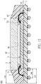
- a sensor package structure 100 i.e., an image sensor package structure 100.
- the sensor package structure 100 includes a substrate 1, a sensor chip 2 disposed on the substrate 1, a plurality of metal wires 3 establishing an electrical connection between the substrate 1 and the sensor chip 2, a translucent layer 4 corresponding in position to the sensor chip 2, and an adhesive 5 firmly adhering the translucent layer 4 to the sensor chip 2 and the substrate 1.
- the following description discloses the structure and connection relationships of each component of the sensor package structure 100.
- the substrate 1 can be a plastic substrate, a ceramic substrate, a lead frame, or a substrate made of other materials, but the present embodiment is not limited thereto.
- the substrate 1 has an upper surface 11 and a lower surface 12 opposite to the upper surface 11.
- the substrate 1 includes a plurality of welding pads 111 formed on the upper surface 11.
- the substrate 1 also includes a plurality of welding pads (not labeled) formed on the lower surface 12 for respectively soldering a plurality of soldering balls (not labeled).
- the substrate 1 of the present embodiment exemplarily has a ball grid array (BGA) arrangement, but the present disclosure is not limited thereto.
- BGA ball grid array
- the sensor chip 2 in the present embodiment is exemplarily an image sensor chip, but the present disclosure is not limited thereto.
- the sensor chip 2 has a top surface 21, a bottom surface 22 opposite to the top surface 21, and a surrounding side 23 perpendicularly connected to the top surface 21 and the bottom surface 22.
- the surrounding side means the side(s) other than the top side and the bottom side.
- the top surface 21 has a sensing region 211 and a spacing region 212 arranged around the sensing region 211.
- the sensing region 211 in the present embodiment is in a square shape or a rectangular shape.
- the center of the sensing region 211 can be the center of the top surface 21 (as shown in Fig.
- the spacing region 212 in the present embodiment is in a square-ring shape, and each portion of the spacing region 212 has the same width. The specific shape of the spacing region 212 can be adjusted according to practical needs.
- the top surface 21 has at least one first edge 213 and at least one second edge 214, and the first edge 213 and the second edge 214 are arranged outside the spacing region 212.
- the surrounding side 23 has at least one side surface 231 connected to the at least one second edge 214.
- a distance D1 between the first edge 213 and the spacing region 212 is greater than a distance D2 between the second edge 214 and the spacing region 212 (as shown in Fig. 5A ).
- the distance D2 is smaller than 1/3-1/4 of the distance D1 (D2 ⁇ 1/3 ⁇ 1/4D1), but the ratio between the distance D1 and the distance D2 can be adjusted according to practical needs.
- the sensor chip 2 includes a plurality of connecting pads 215 formed on a first portion of the top surface 21 between the first edge 213 and the spacing region 212, and a second portion of the top surface 21 between the second edge 214 and the spacing region 212 is provided without any connecting pad 215.
- the top surface 21 can be formed with a plurality of first edges 213 and a single second edge 214 (as shown in Fig. 3 ), or the top surface 21 can also be formed with a plurality of first edges 213 and a plurality of second edges 214 (as shown in Fig. 4 ).
- Fig. 1 can be a cross-sectional view taken along a cross-sectional line IA-IA of Fig. 3 or taken along a cross-sectional line IB-IB of Fig. 4 .
- the top surface 21 can be formed with a single first edge 213 and a plurality of second edges 214.
- the bottom surface 22 of the sensor chip 2 is disposed on the upper surface 11 of the substrate 1, and a portion of the upper surface 11 for mounting the sensor chip 2 is substantially arranged in a region, which is surroundingly defined by the welding pads 111.
- the bottom surface 22 of the sensor chip 2 is fixed on the upper surface 11 of the substrate 1 by using a die attach epoxy (not labeled), but the present disclosure is not limited thereto.
- each metal wire 3 is in a reverse bond mode, and the top surface 21 of the sensor chip 2 and an adjacent portion of each metal wire 3 (i.e., a portion of each metal wire 3 arranged above the top surface 21 as shown in Fig. 1 ) have an angle (not labeled) smaller than or equal to 45 degrees.
- an apex 31 of each metal wire 3 can be located at a lower height for avoiding contact with the translucent layer 4, but the present disclosure is not limited thereto.
- the angle can be smaller than or equal to 30 degrees.
- the translucent layer 4 in the present embodiment is exemplarily a glass plate, but is not limited thereto.
- the translucent layer 4 can be a transparent plate or a semitransparent plate.
- the translucent layer 4 has a first surface 41, a second surface 42 opposite to the first surface 41, and a surrounding side 43 perpendicularly connected to the first surface 41 and the second surface 42.
- the first surface 41 and the second surface 42 have the same square shape or the same rectangular shape, and an area of the second surface 42 is greater than that of the top surface 21 of the sensor chip 2, but the present disclosure is not limited thereto.
- the translucent layer 4 is fixed on the substrate 1 and the sensor chip 2 by using the adhesive 5, and the second surface 42 of the translucent layer 4 is substantially parallel to and faces toward the top surface 21 of the sensor chip 2. Specifically, a projecting area (not labeled) defined by orthogonally projecting the sensor chip 2 onto the second surface 42 is entirely located in the second surface 42.
- the second surface 42 of the translucent layer 4 is arranged adjacent to, but does not contact with, each metal wire 3.
- the apex 31 of each metal wire 3 is arranged outside a space defined by orthogonally projecting the translucent layer 4 to the substrate 1. As shown in Figs.
- a height H1 of the apex 31 of each metal wire 3 with respect to the top surface 21 of the sensor chip 2 is preferably smaller than a height H2 of the second surface 42 of the translucent layer 4 with respect to the top surface 21 of the sensor chip 2, but the present disclosure is not limited thereto.
- the adhesive 5 can be a single piece made of the same material or a composite piece made of different materials, but the present embodiment is not limited thereto.
- the adhesive 5 is disposed on the upper surface 11 of the substrate 1 and covers the surrounding side 23 of the sensor chip 2, the first portion of the top surface 21 between the first edge 213 and the spacing region 212, and the surrounding side 43 and a portion of the second surface 42 of the translucent layer 4. At least part of each of the metal wires 3 and each of the welding pads 111 are embedded in the adhesive 5.
- the adhesive 5 in the present embodiment includes a supporting layer 51, a combining layer 52, and a packaging compound 53, the three of which are connected with each other.
- the material of the supporting layer 51 i.e., a glass mount epoxy
- the material of the packaging compound 53 i.e., a liquid compound
- the following description discloses the connection relationships of each part of the adhesive 5 with respect to the other components.
- the supporting layer 51 in the present embodiment corresponds in shape and position to the second edge 214 of the top surface 21 of the sensor chip 2.
- the supporting layer 51 as shown in Fig. 3 is an elongated structure substantially parallel to the second edge 214, or the supporting layer 51 as shown in Fig. 4 includes two elongated structures respectively parallel to the two second edges 214.
- the supporting layer 51 is arranged adjacent to the second edge 214 of the sensor chip 2 (i.e., the supporting layer 51 contacts the side surface 231 of the sensor chip 2 connected to the second edge 214).
- An edge of the supporting layer 51 i.e., the top edge of the supporting layer 51 as shown in Fig. 5A ) arranged distant from the substrate 1 has a height substantially equal to a height of the top surface 21 (or the second edge 214) of the sensor chip 2.
- an outer side 511 of the supporting layer 51 arranged distant from the sensor chip 2 includes an arc surface 511 having a center of circle (not labeled) located at an interior side of the packaging compound 53 (i.e., the center of circle is located in the supporting layer 51), but the present disclosure in not limited thereto.
- the center of circle (not labeled) of the arc surface 511 can be located in the packaging compound 53.
- the combining layer 52 is substantially in a square ring shape or a rectangular ring shape, and an inner edge of the combining layer 52 is preferably connected to the an outer edge of the spacing region 212 of the sensor chip 2. That is to say, the spacing region 212 is provided for separating the combining layer 52 from the sensing region 211.
- the combining layer 52 is disposed on the supporting layer 51 and the first portion of the top surface 21, the latter of which is disposed between the first edge 213 and the spacing region 212, and a portion of the combining layer 52 disposed on the supporting layer 51 (as shown in Fig.
- the second edge 214 of the top surface 21 is an outer edge of the spacing region 212.
- a width and a height of the portion of the combining layer 52 disposed on the supporting layer 51 are substantially equal to that of a portion of the combining layer 52 disposed on first portion of the top surface 21 (as shown in Fig. 6 ).
- a surrounding side 521 of the combining layer 52 arranged distant from the sensing region 211 includes an arc surface 521 having a center of circle located in the packaging compound 53.
- a largest distance D3 (as shown in Fig. 5A ) between the arc surface 521 of the combining layer 52 and the sensing region 211 is preferably and substantially equal to a distance D4 (as shown in Fig. 6 ) between the first edge 213 and the sensing region 211.
- the arc surface 521 of the combining layer 52 and the arc surface 511 of the supporting layer 51 are in an S-shape, but the present disclosure is not limited thereto (i.e., Fig. 5B ).
- each metal wire 3 is embedded in the combining layer 52.
- each connecting pad 215 and a part of the corresponding metal wire 3 connected thereto in the present embodiment are embedded in the combining layer 52.
- each connecting pad 215 and a part of the corresponding metal wire 3 connected thereto can be not embedded in the combining layer 52.
- a portion the second surface 42 of the translucent layer 4 is adhered to the combining layer 52, so that the second surface 42 of the translucent layer 4, the combining layer 52, and the top surface 21 of the sensor chip 2 surroundingly co-define an enclosed space 6, and the sensing region 211 of the sensor chip 2 is arranged in the enclosed space 6.
- the second surface 42 has a fixing region 421 arranged outside the portion of the second surface 42 adhered to the combining layer 52, and the fixing region 421 is in a square ring shape or a rectangular ring shape.
- the packaging compound 53 is disposed on the upper surface 11 of the substrate 1 and covers the surrounding side 23 of the sensor chip 2, the outer side 511 of the supporting layer 51, the surrounding side 521 of the combining layer 52, and the surrounding side 43 and the fixing region 421 of the translucent layer 4.
- Each of the metal wires 3 in the present embodiment is embedded in the packaging compound 53 and the combining layer 52, and the apex 31 of each of the metal wires 3 is embedded in the packaging compound 53.
- each of the metal wires 3 can be embedded entirely in the packaging compound 53.
- the first surface 41 of the translucent layer 4 and an adjacent surface of the packaging compound 53 i.e., the top surface of the packaging compound 53 as shown in Fig. 1
- the angle ⁇ is preferably within a range of 115 ⁇ 150 degrees.
- a surrounding side surface of the packaging compound 53 other than the top surface and the bottom surface is substantially flush with a surrounding side surface of the substrate 1.
- the packaging compound 53 in the present embodiment is not disposed on the first surface 41 of the translucent layer 4, but the packaging compound 53 in other embodiments of the present disclosure can be disposed on a part of the first surface 41 (i.e., a periphery part of the first surface 41) of the translucent layer 4.
- the sensor chip 2 in the present embodiment which has the second portion provided without any connecting pad 215, can be adapted in the sensor package structure 100. That is to say, the sensor package structure 100 of the present embodiment can be suitable to package the sensor chip 2 which has a smaller size. Furthermore, the sensor package structure 100 can also package the smaller sensor chip 2 by embedding part of each metal wire 3 in the combining layer 52.
- the translucent layer 4 can be firmly fixed at a predetermined position by adhering the packaging compound 53 to the arc surface 511 of the supporting layer 51, the arc surface 521 of the combining layer 52, and the surrounding side 43 and the fixing region 421 of the translucent layer 4. Moreover, the translucent layer 4 can be maintained to not contact each metal wire 3, so that the translucent layer 4 is substantially parallel to the top surface 21 of the sensor chip 2, thereby providing a better reliability of the sensor package structure 100.
- the supporting layer 51 is formed in one process, and the combining layer 52 is later formed in another process, so that the supporting layer 51 is formed to be an extension for a shorter portion of the sensor chip 2 (i.e., the second portion of the top surface 21 between the sensing region 211 and the second edge 214).
- the supporting layer 51 can provide a space sufficient to receive the combining layer 52, preventing the combining layer 52 from contacting the sensing region 211.
- the sensor package structure 100 as shown in Figs. 1 to 6 can be adjusted according to practical needs, but as the present disclosure cannot disclose all varieties of configurations, the following description will only disclose some exemplary configurations of the sensor package structure 100.
- the surrounding side 43 of the translucent layer 4 is in a step shape and is embedded in the packaging compound 53.
- An area of the first surface 41 is smaller than that of the second surface 42.
- the area of the first surface 41 can be greater than that of the second surface 42.
- the sensor package structure 100 can further include a molding compound 54 disposed on a top surface of the packaging compound 53.
- a top surface of the molding compound 54 is substantially parallel to the first surface 41 of the translucent layer 41, and a surrounding side surface of the molding compound 54 other than the top surface and the bottom surface is coplanar with a surrounding side surface of the packaging compound 53, but the present disclosure is not limited thereto.
- the top surface of the molding compound 54 can be substantially coplanar with the first surface 41 of the translucent layer 41.
- the packaging compound 53 can be a molding compound, and the first surface 41 of the translucent layer 4 is substantially parallel to an adjacent surface of the packaging compound 53. Moreover, the first surface 41 of the translucent layer 4 and the adjacent surface of the packaging compound 53 preferably have an angle ⁇ of 180 degrees.
- Fig. 10 illustrates a second embodiment of the present disclosure.
- the present embodiment is similar to the first embodiment, except that in the second embodiment, the combining layer 52 and the supporting layer 51 are replaced by a first combining layer 55 and a second combining layer 56.
- the supporting layer 51 and a portion of the combining layer 52 disposed on the supporting layer 51 (as shown in Fig. 5 ) as disclosed in the first embodiment are adjusted to be formed in one process and are co-defined as the second combining layer 56, and the other portion of the combining layer 52 (as shown in Fig. 6 ) is adjusted to be formed in another process and is defined as the first combining layer 55, but the present disclosure is not limited thereto.
- the structural features of the present embodiment different from the first embodiment are disclosed as follows.
- the first combining layer 55 is disposed on the first portion of the top surface 21 between the first edge 213 and the spacing region 212.
- the second combining layer 56 is disposed on the upper surface 11 of the substrate 1 and is arranged adjacent to the second edge 214 of the sensor chip 2 (i.e., the second combining layer 56 contacts the side surface 231 of the sensor chip 2).
- the second combining layer 56 can be further disposed on the second portion of the top surface 21 between the second edge 214 and the spacing region 212, and an area of the second portion of the top surface 21 is smaller than that of a portion of the spacing region 212 connected to the second portion of the top surface 21.
- a height of the second combining layer 56 with respect to the upper surface 11 of the substrate 1 is substantially equal to that of the first combining layer 55 with respect to the upper surface 11 of the substrate 1.
- a largest distance between an upper half of an outer side 561 of the second combining layer 56 and the sensing region 211 is substantially equal to a distance between the first edge 213 and the sensing region 211.
- An outer side 551 of the first combining layer 55 arranged distant from the sensing region 211 includes an arc surface 551 having a center of circle located in the packaging compound 53.
- the outer side 561 of the second combining layer 56 arranged distant from the sensor chip 2 is in an S-shape, but the present disclosure is not limited thereto (e.g., Fig. 5B ).
- a portion of the second surface 42 of the translucent layer 4 is adhered to the first combining layer 55 and the second combining layer 56.
- the second surface 42 has a fixing region 421 arranged outside the portion of the second surface 42 adhered to the first combining layer 55 and the second combining layer 56.
- the packaging compound 53 is disposed on the upper surface 11 of the substrate 1 and covers the surrounding side 23 of the sensor chip 2, the outer side 551 of the first combining layer 55, the outer side 561 of the second combining layer 56, and the surrounding side 43 and the fixing region 421 of the translucent layer 4. A part of each metal wire 3 and each welding pad 111 are embedded in the packaging compound 53.
- Figs. 11 and 12 illustrate a third embodiment of the present disclosure.
- the present embodiment is similar to the first embodiment, except that the sensor package structure 100 of the third embodiment is provided without any supporting layer 51; that is to say, the edges of the top surface 21 of the sensor chip 2 in the present embodiment are first edges 213.
- a distance D5 between the surrounding side 43 of the translucent layer 4 and an adjacent side of the packaging compound 53 is substantially 300 ⁇ 500 ⁇ m
- a largest distance D6 between a surrounding side of each of the welding pads 111 and an adjacent portion of the surrounding side 23 of the sensor chip 2 is substantially 200 ⁇ 350 ⁇ m
- a distance D7 between the portion of the surrounding side 23 of the sensor chip 2 adjacent to at least one of the welding pads 111 and an adjacent side surface of the packaging compound 53 is substantially 375 ⁇ 575 ⁇ m.
- the size of the sensor package structure 100 is smaller than that of the conventional sensor package structure, and the amount of the packing compound 53 of the sensor package structure 100 is less than that of the conventional sensor package structure, so that the thermal expansion and contraction of the packaging compound 53 generates less stress to the sensor package structure 100, thereby increasing the reliability of the sensor package structure 100.
Landscapes
- Solid State Image Pick-Up Elements (AREA)
- Light Receiving Elements (AREA)
Applications Claiming Priority (2)
| Application Number | Priority Date | Filing Date | Title |
|---|---|---|---|
| US201662358643P | 2016-07-06 | 2016-07-06 | |
| CN201610868068.0A CN107591374B (zh) | 2016-07-06 | 2016-09-30 | 感测器封装结构 |
Publications (2)
| Publication Number | Publication Date |
|---|---|
| EP3267486A1 true EP3267486A1 (de) | 2018-01-10 |
| EP3267486B1 EP3267486B1 (de) | 2020-12-30 |
Family
ID=59276540
Family Applications (1)
| Application Number | Title | Priority Date | Filing Date |
|---|---|---|---|
| EP17178914.2A Active EP3267486B1 (de) | 2016-07-06 | 2017-06-30 | Sensorgehäusestruktur |
Country Status (3)
| Country | Link |
|---|---|
| US (1) | US10236313B2 (de) |
| EP (1) | EP3267486B1 (de) |
| JP (1) | JP6479099B2 (de) |
Cited By (2)
| Publication number | Priority date | Publication date | Assignee | Title |
|---|---|---|---|---|
| CN111769125A (zh) * | 2019-04-02 | 2020-10-13 | 胜丽国际股份有限公司 | 感测器封装结构 |
| US20210265225A1 (en) * | 2020-02-21 | 2021-08-26 | Amkor Technology Singapore Holding Pte. Ltd. | Semiconductor devices and methods of manufacturing semiconductor devices |
Families Citing this family (5)
| Publication number | Priority date | Publication date | Assignee | Title |
|---|---|---|---|---|
| US10692917B2 (en) * | 2016-07-06 | 2020-06-23 | Kingpak Technology Inc. | Sensor package structure |
| TWI769780B (zh) * | 2021-04-12 | 2022-07-01 | 勝麗國際股份有限公司 | 感測器封裝結構 |
| JPWO2024053466A1 (de) * | 2022-09-09 | 2024-03-14 | ||
| CN116259636A (zh) * | 2022-09-09 | 2023-06-13 | 积高电子(无锡)有限公司 | 一种图像传感器的封装结构 |
| WO2026063182A1 (ja) * | 2024-09-18 | 2026-03-26 | ソニーセミコンダクタソリューションズ株式会社 | 半導体装置、半導体装置の製造方法 |
Citations (3)
| Publication number | Priority date | Publication date | Assignee | Title |
|---|---|---|---|---|
| WO2006101270A1 (en) * | 2005-03-25 | 2006-09-28 | Fujifilm Corporation | Solid state imaging device and manufacturing method thereof |
| US20090267170A1 (en) * | 2008-04-29 | 2009-10-29 | Omnivision Technologies, Inc. | Apparatus and Method For Using Spacer Paste to Package an Image Sensor |
| EP2492961A2 (de) * | 2011-02-24 | 2012-08-29 | Kingpak Technology Inc. | Verfahren zur Reduzierung der Verkippung eines transparenten Fensters während der Herstellung eines Bildsensors |
Family Cites Families (10)
| Publication number | Priority date | Publication date | Assignee | Title |
|---|---|---|---|---|
| JPH03229435A (ja) * | 1990-02-05 | 1991-10-11 | Matsushita Electric Ind Co Ltd | ワイヤーボンディング用キャピラリ |
| US5468999A (en) * | 1994-05-26 | 1995-11-21 | Motorola, Inc. | Liquid encapsulated ball grid array semiconductor device with fine pitch wire bonding |
| JP2002076154A (ja) * | 2000-08-23 | 2002-03-15 | Kyocera Corp | 半導体装置 |
| JP5095113B2 (ja) * | 2005-03-25 | 2012-12-12 | 富士フイルム株式会社 | 固体撮像装置の製造方法、及び固体撮像装置 |
| TWI285417B (en) | 2005-10-17 | 2007-08-11 | Taiwan Electronic Packaging Co | Image chip package structure and packaging method thereof |
| KR101100790B1 (ko) * | 2006-09-15 | 2012-01-02 | 후지쯔 세미컨덕터 가부시키가이샤 | 반도체 장치 및 그 제조 방법 |
| TWI305036B (en) * | 2006-09-28 | 2009-01-01 | Siliconware Precision Industries Co Ltd | Sensor-type package structure and fabrication method thereof |
| TW201104850A (en) * | 2009-07-29 | 2011-02-01 | Kingpak Tech Inc | Image sensor package structure with large air cavity |
| JP5818455B2 (ja) * | 2011-02-17 | 2015-11-18 | キヤノン株式会社 | 固体撮像装置およびその製造方法 |
| TW201503334A (zh) * | 2013-07-08 | 2015-01-16 | 勝開科技股份有限公司 | 影像感測器二階段封裝方法 |
-
2017
- 2017-06-30 EP EP17178914.2A patent/EP3267486B1/de active Active
- 2017-07-04 JP JP2017131010A patent/JP6479099B2/ja active Active
- 2017-07-05 US US15/641,401 patent/US10236313B2/en active Active
Patent Citations (3)
| Publication number | Priority date | Publication date | Assignee | Title |
|---|---|---|---|---|
| WO2006101270A1 (en) * | 2005-03-25 | 2006-09-28 | Fujifilm Corporation | Solid state imaging device and manufacturing method thereof |
| US20090267170A1 (en) * | 2008-04-29 | 2009-10-29 | Omnivision Technologies, Inc. | Apparatus and Method For Using Spacer Paste to Package an Image Sensor |
| EP2492961A2 (de) * | 2011-02-24 | 2012-08-29 | Kingpak Technology Inc. | Verfahren zur Reduzierung der Verkippung eines transparenten Fensters während der Herstellung eines Bildsensors |
Cited By (3)
| Publication number | Priority date | Publication date | Assignee | Title |
|---|---|---|---|---|
| CN111769125A (zh) * | 2019-04-02 | 2020-10-13 | 胜丽国际股份有限公司 | 感测器封装结构 |
| US20210265225A1 (en) * | 2020-02-21 | 2021-08-26 | Amkor Technology Singapore Holding Pte. Ltd. | Semiconductor devices and methods of manufacturing semiconductor devices |
| US11908755B2 (en) * | 2020-02-21 | 2024-02-20 | Amkor Technology Singapore Holding Pte. Ltd. | Semiconductor devices and methods of manufacturing semiconductor devices |
Also Published As
| Publication number | Publication date |
|---|---|
| US10236313B2 (en) | 2019-03-19 |
| EP3267486B1 (de) | 2020-12-30 |
| JP6479099B2 (ja) | 2019-03-06 |
| JP2018006760A (ja) | 2018-01-11 |
| US20180012920A1 (en) | 2018-01-11 |
Similar Documents
| Publication | Publication Date | Title |
|---|---|---|
| US10186538B2 (en) | Sensor package structure | |
| EP3267486A1 (de) | Sensorgehäusestruktur | |
| US10692917B2 (en) | Sensor package structure | |
| US10600830B2 (en) | Sensor package structure | |
| CN107591374B (zh) | 感测器封装结构 | |
| US9929075B2 (en) | Chip-scale electronic package structure with conductive connective element having increased surface area and laterally spaced connection points for improved connectivity | |
| CN111048534B (zh) | 感测器封装结构 | |
| JP2019501534A (ja) | 改良された補剛材を有する積層シリコンパッケージアセンブリ | |
| US6262479B1 (en) | Semiconductor packaging structure | |
| US9633932B2 (en) | Lead frame package having discharge hole and method of manufacturing the same | |
| US20050212108A1 (en) | Semiconductor chip package | |
| EP3628776B1 (de) | Sensorpaketstruktur | |
| EP3260821B1 (de) | Sensorpaket und verfahren zur herstellung des sensorpakets | |
| CN115206893B (zh) | 传感器封装结构 | |
| US20070277607A1 (en) | Semiconductor acceleration sensor | |
| US9219026B2 (en) | Semiconductor device | |
| CN112038299B (zh) | 堆叠式感测器封装结构 | |
| US8519522B2 (en) | Semiconductor package | |
| US7233060B2 (en) | Module card structure | |
| CN102569217B (zh) | 半导体封装件 | |
| US7838981B2 (en) | Component assembly | |
| JP2003318362A (ja) | 樹脂封止形半導体装置 | |
| US7345356B2 (en) | Optical package with double formed leadframe | |
| JP2009094246A (ja) | 半導体装置 |
Legal Events
| Date | Code | Title | Description |
|---|---|---|---|
| PUAI | Public reference made under article 153(3) epc to a published international application that has entered the european phase |
Free format text: ORIGINAL CODE: 0009012 |
|
| STAA | Information on the status of an ep patent application or granted ep patent |
Free format text: STATUS: THE APPLICATION HAS BEEN PUBLISHED |
|
| AK | Designated contracting states |
Kind code of ref document: A1 Designated state(s): AL AT BE BG CH CY CZ DE DK EE ES FI FR GB GR HR HU IE IS IT LI LT LU LV MC MK MT NL NO PL PT RO RS SE SI SK SM TR |
|
| AX | Request for extension of the european patent |
Extension state: BA ME |
|
| STAA | Information on the status of an ep patent application or granted ep patent |
Free format text: STATUS: REQUEST FOR EXAMINATION WAS MADE |
|
| 17P | Request for examination filed |
Effective date: 20180405 |
|
| RBV | Designated contracting states (corrected) |
Designated state(s): AL AT BE BG CH CY CZ DE DK EE ES FI FR GB GR HR HU IE IS IT LI LT LU LV MC MK MT NL NO PL PT RO RS SE SI SK SM TR |
|
| STAA | Information on the status of an ep patent application or granted ep patent |
Free format text: STATUS: EXAMINATION IS IN PROGRESS |
|
| 17Q | First examination report despatched |
Effective date: 20191122 |
|
| GRAP | Despatch of communication of intention to grant a patent |
Free format text: ORIGINAL CODE: EPIDOSNIGR1 |
|
| STAA | Information on the status of an ep patent application or granted ep patent |
Free format text: STATUS: GRANT OF PATENT IS INTENDED |
|
| INTG | Intention to grant announced |
Effective date: 20200724 |
|
| GRAS | Grant fee paid |
Free format text: ORIGINAL CODE: EPIDOSNIGR3 |
|
| GRAA | (expected) grant |
Free format text: ORIGINAL CODE: 0009210 |
|
| STAA | Information on the status of an ep patent application or granted ep patent |
Free format text: STATUS: THE PATENT HAS BEEN GRANTED |
|
| RAP1 | Party data changed (applicant data changed or rights of an application transferred) |
Owner name: KINGPAK TECHNOLOGY INC. |
|
| AK | Designated contracting states |
Kind code of ref document: B1 Designated state(s): AL AT BE BG CH CY CZ DE DK EE ES FI FR GB GR HR HU IE IS IT LI LT LU LV MC MK MT NL NO PL PT RO RS SE SI SK SM TR |
|
| REG | Reference to a national code |
Ref country code: GB Ref legal event code: FG4D |
|
| REG | Reference to a national code |
Ref country code: AT Ref legal event code: REF Ref document number: 1350796 Country of ref document: AT Kind code of ref document: T Effective date: 20210115 |
|
| REG | Reference to a national code |
Ref country code: DE Ref legal event code: R096 Ref document number: 602017030325 Country of ref document: DE |
|
| REG | Reference to a national code |
Ref country code: IE Ref legal event code: FG4D |
|
| PG25 | Lapsed in a contracting state [announced via postgrant information from national office to epo] |
Ref country code: RS Free format text: LAPSE BECAUSE OF FAILURE TO SUBMIT A TRANSLATION OF THE DESCRIPTION OR TO PAY THE FEE WITHIN THE PRESCRIBED TIME-LIMIT Effective date: 20201230 Ref country code: NO Free format text: LAPSE BECAUSE OF FAILURE TO SUBMIT A TRANSLATION OF THE DESCRIPTION OR TO PAY THE FEE WITHIN THE PRESCRIBED TIME-LIMIT Effective date: 20210330 Ref country code: FI Free format text: LAPSE BECAUSE OF FAILURE TO SUBMIT A TRANSLATION OF THE DESCRIPTION OR TO PAY THE FEE WITHIN THE PRESCRIBED TIME-LIMIT Effective date: 20201230 Ref country code: GR Free format text: LAPSE BECAUSE OF FAILURE TO SUBMIT A TRANSLATION OF THE DESCRIPTION OR TO PAY THE FEE WITHIN THE PRESCRIBED TIME-LIMIT Effective date: 20210331 |
|
| REG | Reference to a national code |
Ref country code: AT Ref legal event code: MK05 Ref document number: 1350796 Country of ref document: AT Kind code of ref document: T Effective date: 20201230 |
|
| PG25 | Lapsed in a contracting state [announced via postgrant information from national office to epo] |
Ref country code: SE Free format text: LAPSE BECAUSE OF FAILURE TO SUBMIT A TRANSLATION OF THE DESCRIPTION OR TO PAY THE FEE WITHIN THE PRESCRIBED TIME-LIMIT Effective date: 20201230 Ref country code: BG Free format text: LAPSE BECAUSE OF FAILURE TO SUBMIT A TRANSLATION OF THE DESCRIPTION OR TO PAY THE FEE WITHIN THE PRESCRIBED TIME-LIMIT Effective date: 20210330 Ref country code: LV Free format text: LAPSE BECAUSE OF FAILURE TO SUBMIT A TRANSLATION OF THE DESCRIPTION OR TO PAY THE FEE WITHIN THE PRESCRIBED TIME-LIMIT Effective date: 20201230 |
|
| REG | Reference to a national code |
Ref country code: NL Ref legal event code: MP Effective date: 20201230 |
|
| PG25 | Lapsed in a contracting state [announced via postgrant information from national office to epo] |
Ref country code: HR Free format text: LAPSE BECAUSE OF FAILURE TO SUBMIT A TRANSLATION OF THE DESCRIPTION OR TO PAY THE FEE WITHIN THE PRESCRIBED TIME-LIMIT Effective date: 20201230 |
|
| REG | Reference to a national code |
Ref country code: LT Ref legal event code: MG9D |
|
| PG25 | Lapsed in a contracting state [announced via postgrant information from national office to epo] |
Ref country code: LT Free format text: LAPSE BECAUSE OF FAILURE TO SUBMIT A TRANSLATION OF THE DESCRIPTION OR TO PAY THE FEE WITHIN THE PRESCRIBED TIME-LIMIT Effective date: 20201230 Ref country code: EE Free format text: LAPSE BECAUSE OF FAILURE TO SUBMIT A TRANSLATION OF THE DESCRIPTION OR TO PAY THE FEE WITHIN THE PRESCRIBED TIME-LIMIT Effective date: 20201230 Ref country code: CZ Free format text: LAPSE BECAUSE OF FAILURE TO SUBMIT A TRANSLATION OF THE DESCRIPTION OR TO PAY THE FEE WITHIN THE PRESCRIBED TIME-LIMIT Effective date: 20201230 Ref country code: PT Free format text: LAPSE BECAUSE OF FAILURE TO SUBMIT A TRANSLATION OF THE DESCRIPTION OR TO PAY THE FEE WITHIN THE PRESCRIBED TIME-LIMIT Effective date: 20210430 Ref country code: RO Free format text: LAPSE BECAUSE OF FAILURE TO SUBMIT A TRANSLATION OF THE DESCRIPTION OR TO PAY THE FEE WITHIN THE PRESCRIBED TIME-LIMIT Effective date: 20201230 Ref country code: SK Free format text: LAPSE BECAUSE OF FAILURE TO SUBMIT A TRANSLATION OF THE DESCRIPTION OR TO PAY THE FEE WITHIN THE PRESCRIBED TIME-LIMIT Effective date: 20201230 |
|
| PG25 | Lapsed in a contracting state [announced via postgrant information from national office to epo] |
Ref country code: AT Free format text: LAPSE BECAUSE OF FAILURE TO SUBMIT A TRANSLATION OF THE DESCRIPTION OR TO PAY THE FEE WITHIN THE PRESCRIBED TIME-LIMIT Effective date: 20201230 Ref country code: PL Free format text: LAPSE BECAUSE OF FAILURE TO SUBMIT A TRANSLATION OF THE DESCRIPTION OR TO PAY THE FEE WITHIN THE PRESCRIBED TIME-LIMIT Effective date: 20201230 |
|
| PG25 | Lapsed in a contracting state [announced via postgrant information from national office to epo] |
Ref country code: IS Free format text: LAPSE BECAUSE OF FAILURE TO SUBMIT A TRANSLATION OF THE DESCRIPTION OR TO PAY THE FEE WITHIN THE PRESCRIBED TIME-LIMIT Effective date: 20210430 |
|
| REG | Reference to a national code |
Ref country code: DE Ref legal event code: R097 Ref document number: 602017030325 Country of ref document: DE |
|
| PG25 | Lapsed in a contracting state [announced via postgrant information from national office to epo] |
Ref country code: AL Free format text: LAPSE BECAUSE OF FAILURE TO SUBMIT A TRANSLATION OF THE DESCRIPTION OR TO PAY THE FEE WITHIN THE PRESCRIBED TIME-LIMIT Effective date: 20201230 Ref country code: IT Free format text: LAPSE BECAUSE OF FAILURE TO SUBMIT A TRANSLATION OF THE DESCRIPTION OR TO PAY THE FEE WITHIN THE PRESCRIBED TIME-LIMIT Effective date: 20201230 |
|
| PLBE | No opposition filed within time limit |
Free format text: ORIGINAL CODE: 0009261 |
|
| STAA | Information on the status of an ep patent application or granted ep patent |
Free format text: STATUS: NO OPPOSITION FILED WITHIN TIME LIMIT |
|
| PG25 | Lapsed in a contracting state [announced via postgrant information from national office to epo] |
Ref country code: DK Free format text: LAPSE BECAUSE OF FAILURE TO SUBMIT A TRANSLATION OF THE DESCRIPTION OR TO PAY THE FEE WITHIN THE PRESCRIBED TIME-LIMIT Effective date: 20201230 |
|
| 26N | No opposition filed |
Effective date: 20211001 |
|
| PG25 | Lapsed in a contracting state [announced via postgrant information from national office to epo] |
Ref country code: ES Free format text: LAPSE BECAUSE OF FAILURE TO SUBMIT A TRANSLATION OF THE DESCRIPTION OR TO PAY THE FEE WITHIN THE PRESCRIBED TIME-LIMIT Effective date: 20201230 Ref country code: MC Free format text: LAPSE BECAUSE OF FAILURE TO SUBMIT A TRANSLATION OF THE DESCRIPTION OR TO PAY THE FEE WITHIN THE PRESCRIBED TIME-LIMIT Effective date: 20201230 |
|
| REG | Reference to a national code |
Ref country code: CH Ref legal event code: PL |
|
| PG25 | Lapsed in a contracting state [announced via postgrant information from national office to epo] |
Ref country code: SI Free format text: LAPSE BECAUSE OF FAILURE TO SUBMIT A TRANSLATION OF THE DESCRIPTION OR TO PAY THE FEE WITHIN THE PRESCRIBED TIME-LIMIT Effective date: 20201230 |
|
| REG | Reference to a national code |
Ref country code: BE Ref legal event code: MM Effective date: 20210630 |
|
| PG25 | Lapsed in a contracting state [announced via postgrant information from national office to epo] |
Ref country code: LU Free format text: LAPSE BECAUSE OF NON-PAYMENT OF DUE FEES Effective date: 20210630 |
|
| PG25 | Lapsed in a contracting state [announced via postgrant information from national office to epo] |
Ref country code: LI Free format text: LAPSE BECAUSE OF NON-PAYMENT OF DUE FEES Effective date: 20210630 Ref country code: IE Free format text: LAPSE BECAUSE OF NON-PAYMENT OF DUE FEES Effective date: 20210630 Ref country code: CH Free format text: LAPSE BECAUSE OF NON-PAYMENT OF DUE FEES Effective date: 20210630 |
|
| PG25 | Lapsed in a contracting state [announced via postgrant information from national office to epo] |
Ref country code: IS Free format text: LAPSE BECAUSE OF FAILURE TO SUBMIT A TRANSLATION OF THE DESCRIPTION OR TO PAY THE FEE WITHIN THE PRESCRIBED TIME-LIMIT Effective date: 20210430 Ref country code: FR Free format text: LAPSE BECAUSE OF NON-PAYMENT OF DUE FEES Effective date: 20210630 |
|
| PG25 | Lapsed in a contracting state [announced via postgrant information from national office to epo] |
Ref country code: BE Free format text: LAPSE BECAUSE OF NON-PAYMENT OF DUE FEES Effective date: 20210630 |
|
| REG | Reference to a national code |
Ref country code: DE Ref legal event code: R081 Ref document number: 602017030325 Country of ref document: DE Owner name: TONG HSING ELECTRONIC INDUSTRIES., LTD., TW Free format text: FORMER OWNER: KINGPAK TECHNOLOGY INC., CHUPEI, HSINCHU, TW |
|
| REG | Reference to a national code |
Ref country code: GB Ref legal event code: 732E Free format text: REGISTERED BETWEEN 20230105 AND 20230111 |
|
| PG25 | Lapsed in a contracting state [announced via postgrant information from national office to epo] |
Ref country code: HU Free format text: LAPSE BECAUSE OF FAILURE TO SUBMIT A TRANSLATION OF THE DESCRIPTION OR TO PAY THE FEE WITHIN THE PRESCRIBED TIME-LIMIT; INVALID AB INITIO Effective date: 20170630 |
|
| PG25 | Lapsed in a contracting state [announced via postgrant information from national office to epo] |
Ref country code: NL Free format text: LAPSE BECAUSE OF NON-PAYMENT OF DUE FEES Effective date: 20201230 Ref country code: CY Free format text: LAPSE BECAUSE OF FAILURE TO SUBMIT A TRANSLATION OF THE DESCRIPTION OR TO PAY THE FEE WITHIN THE PRESCRIBED TIME-LIMIT Effective date: 20201230 |
|
| PG25 | Lapsed in a contracting state [announced via postgrant information from national office to epo] |
Ref country code: SM Free format text: LAPSE BECAUSE OF FAILURE TO SUBMIT A TRANSLATION OF THE DESCRIPTION OR TO PAY THE FEE WITHIN THE PRESCRIBED TIME-LIMIT Effective date: 20201230 |
|
| PG25 | Lapsed in a contracting state [announced via postgrant information from national office to epo] |
Ref country code: MK Free format text: LAPSE BECAUSE OF FAILURE TO SUBMIT A TRANSLATION OF THE DESCRIPTION OR TO PAY THE FEE WITHIN THE PRESCRIBED TIME-LIMIT Effective date: 20201230 |
|
| PG25 | Lapsed in a contracting state [announced via postgrant information from national office to epo] |
Ref country code: TR Free format text: LAPSE BECAUSE OF FAILURE TO SUBMIT A TRANSLATION OF THE DESCRIPTION OR TO PAY THE FEE WITHIN THE PRESCRIBED TIME-LIMIT Effective date: 20201230 |
|
| PG25 | Lapsed in a contracting state [announced via postgrant information from national office to epo] |
Ref country code: MT Free format text: LAPSE BECAUSE OF FAILURE TO SUBMIT A TRANSLATION OF THE DESCRIPTION OR TO PAY THE FEE WITHIN THE PRESCRIBED TIME-LIMIT Effective date: 20201230 |
|
| REG | Reference to a national code |
Ref country code: DE Ref legal event code: R079 Ref document number: 602017030325 Country of ref document: DE Free format text: PREVIOUS MAIN CLASS: H01L0027146000 Ipc: H10F0039180000 |
|
| PGFP | Annual fee paid to national office [announced via postgrant information from national office to epo] |
Ref country code: DE Payment date: 20250627 Year of fee payment: 9 |
|
| PGFP | Annual fee paid to national office [announced via postgrant information from national office to epo] |
Ref country code: GB Payment date: 20250627 Year of fee payment: 9 |