EP3270232B1 - Beobachtungsvorrichtung für eine probe - Google Patents
Beobachtungsvorrichtung für eine probe Download PDFInfo
- Publication number
- EP3270232B1 EP3270232B1 EP17180937.9A EP17180937A EP3270232B1 EP 3270232 B1 EP3270232 B1 EP 3270232B1 EP 17180937 A EP17180937 A EP 17180937A EP 3270232 B1 EP3270232 B1 EP 3270232B1
- Authority
- EP
- European Patent Office
- Prior art keywords
- sample
- light
- light source
- image sensor
- micron
- Prior art date
- Legal status (The legal status is an assumption and is not a legal conclusion. Google has not performed a legal analysis and makes no representation as to the accuracy of the status listed.)
- Active
Links
Images


Classifications
-
- G—PHYSICS
- G03—PHOTOGRAPHY; CINEMATOGRAPHY; ANALOGOUS TECHNIQUES USING WAVES OTHER THAN OPTICAL WAVES; ELECTROGRAPHY; HOLOGRAPHY
- G03H—HOLOGRAPHIC PROCESSES OR APPARATUS
- G03H1/00—Holographic processes or apparatus using light, infrared or ultraviolet waves for obtaining holograms or for obtaining an image from them; Details peculiar thereto
- G03H1/04—Processes or apparatus for producing holograms
- G03H1/0465—Particular recording light; Beam shape or geometry
-
- G—PHYSICS
- G03—PHOTOGRAPHY; CINEMATOGRAPHY; ANALOGOUS TECHNIQUES USING WAVES OTHER THAN OPTICAL WAVES; ELECTROGRAPHY; HOLOGRAPHY
- G03H—HOLOGRAPHIC PROCESSES OR APPARATUS
- G03H1/00—Holographic processes or apparatus using light, infrared or ultraviolet waves for obtaining holograms or for obtaining an image from them; Details peculiar thereto
- G03H1/04—Processes or apparatus for producing holograms
- G03H1/0402—Recording geometries or arrangements
- G03H1/0404—In-line recording arrangement
-
- G—PHYSICS
- G03—PHOTOGRAPHY; CINEMATOGRAPHY; ANALOGOUS TECHNIQUES USING WAVES OTHER THAN OPTICAL WAVES; ELECTROGRAPHY; HOLOGRAPHY
- G03H—HOLOGRAPHIC PROCESSES OR APPARATUS
- G03H1/00—Holographic processes or apparatus using light, infrared or ultraviolet waves for obtaining holograms or for obtaining an image from them; Details peculiar thereto
- G03H1/04—Processes or apparatus for producing holograms
- G03H1/0443—Digital holography, i.e. recording holograms with digital recording means
-
- G—PHYSICS
- G01—MEASURING; TESTING
- G01N—INVESTIGATING OR ANALYSING MATERIALS BY DETERMINING THEIR CHEMICAL OR PHYSICAL PROPERTIES
- G01N15/00—Investigating characteristics of particles; Investigating permeability, pore-volume or surface-area of porous materials
- G01N15/10—Investigating individual particles
- G01N15/14—Optical investigation techniques, e.g. flow cytometry
- G01N15/1434—Optical arrangements
- G01N2015/1454—Optical arrangements using phase shift or interference, e.g. for improving contrast
-
- G—PHYSICS
- G01—MEASURING; TESTING
- G01N—INVESTIGATING OR ANALYSING MATERIALS BY DETERMINING THEIR CHEMICAL OR PHYSICAL PROPERTIES
- G01N21/00—Investigating or analysing materials by the use of optical means, i.e. using sub-millimetre waves, infrared, visible or ultraviolet light
- G01N21/17—Systems in which incident light is modified in accordance with the properties of the material investigated
- G01N21/41—Refractivity; Phase-affecting properties, e.g. optical path length
- G01N21/45—Refractivity; Phase-affecting properties, e.g. optical path length using interferometric methods; using Schlieren methods
- G01N21/453—Holographic interferometry
-
- G—PHYSICS
- G03—PHOTOGRAPHY; CINEMATOGRAPHY; ANALOGOUS TECHNIQUES USING WAVES OTHER THAN OPTICAL WAVES; ELECTROGRAPHY; HOLOGRAPHY
- G03H—HOLOGRAPHIC PROCESSES OR APPARATUS
- G03H1/00—Holographic processes or apparatus using light, infrared or ultraviolet waves for obtaining holograms or for obtaining an image from them; Details peculiar thereto
- G03H1/04—Processes or apparatus for producing holograms
- G03H1/0443—Digital holography, i.e. recording holograms with digital recording means
- G03H2001/0447—In-line recording arrangement
-
- G—PHYSICS
- G03—PHOTOGRAPHY; CINEMATOGRAPHY; ANALOGOUS TECHNIQUES USING WAVES OTHER THAN OPTICAL WAVES; ELECTROGRAPHY; HOLOGRAPHY
- G03H—HOLOGRAPHIC PROCESSES OR APPARATUS
- G03H2222/00—Light sources or light beam properties
- G03H2222/10—Spectral composition
- G03H2222/12—Single or narrow bandwidth source, e.g. laser, light emitting diode [LED]
-
- G—PHYSICS
- G03—PHOTOGRAPHY; CINEMATOGRAPHY; ANALOGOUS TECHNIQUES USING WAVES OTHER THAN OPTICAL WAVES; ELECTROGRAPHY; HOLOGRAPHY
- G03H—HOLOGRAPHIC PROCESSES OR APPARATUS
- G03H2222/00—Light sources or light beam properties
- G03H2222/20—Coherence of the light source
- G03H2222/24—Low coherence light normally not allowing valuable record or reconstruction
-
- G—PHYSICS
- G03—PHOTOGRAPHY; CINEMATOGRAPHY; ANALOGOUS TECHNIQUES USING WAVES OTHER THAN OPTICAL WAVES; ELECTROGRAPHY; HOLOGRAPHY
- G03H—HOLOGRAPHIC PROCESSES OR APPARATUS
- G03H2223/00—Optical components
- G03H2223/12—Amplitude mask, e.g. diaphragm, Louver filter
Definitions
- the technical field of the invention is the observation of a sample by forming a hologram of the sample using an image sensor.
- This image is formed by interference patterns between the light wave emitted by the source and transmitted by the sample, and diffraction waves, resulting from the diffraction by the sample of the light wave emitted by the source. These interference patterns are sometimes called diffraction patterns, or designated by the English term "diffraction pattern".
- the image formed on the image sensor can be processed by a digital propagation algorithm, so as to estimate the optical properties of the sample. Such algorithms are well known in the field of holographic reconstruction. For this, the distance between the sample and the image sensor being known, a holographic reconstruction algorithm is applied, taking this distance into account.
- the document WO2008090330 showed that by replacing the laser light source with a spatially filtered light-emitting diode, it was possible to obtain a usable image of biological samples, in this case cells, by lensless imaging.
- the device described in this document makes it possible to associate, with each cell, an interference pattern whose morphology makes it possible to identify the cell type.
- the light source is a light-emitting diode associated with a diaphragm, forming an opening, the opening being designated by the terms "aperture" or "pin hole”.
- the presence of such a spatial filter had certain drawbacks. On the one hand, it requires precise centering of the light source relative to the aperture it defines. In addition, this centering must remain precise during the implementation of the device, in particular during its handling or transport. Furthermore, the presence of a spatial filter requires a compromise to be made at the level of the filter aperture. A small aperture allows good spatial coherence to be obtained, but considerably limits the solid angle of emission of the incident light wave, which reduces the quantity of light reaching the detector. This is detrimental to the sensitivity of the measurement. The inventors propose a device to overcome these drawbacks.
- An object of the invention is a device for observing a sample according to claim 1.
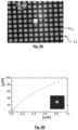
- the light source may comprise a plurality of micrometric light-emitting diodes.
- the micrometric light-emitting diodes may then be arranged in a matrix, being spaced apart from each other by a distance of less than 50 ⁇ m.
- the micrometric light-emitting diodes may have different spectral emission bands from each other and/or may be capable of being activated successively or simultaneously.
- the micrometric light-emitting diodes may be capable of being activated independently of each other.
- Another object of the invention is a method of observing a sample according to claim 7.
- the micrometric light-emitting diode can in particular have an optical emission power greater than 50 ⁇ W.
- the light source may comprise a plurality of micrometer light-emitting diodes.
- the micrometer light-emitting diodes may then be arranged in a matrix, being spaced apart from each other by a distance of less than 50 ⁇ m.
- the micrometer light-emitting diodes may have different emission spectral bands from each other and/or may be capable of being activated successively or simultaneously.
- the micrometer light-emitting diodes may be capable of being activated independently of each other.
- the largest diameter or diagonal of the micrometer light-emitting diode is less than 150 ⁇ m or 50 ⁇ m.
- the light source comprises a plurality of micrometric light-emitting diodes.
- the micrometric light-emitting diodes can then be activated simultaneously or independently of one another or successively.
- the image sensor can acquire an image during each successive activation.
- the micrometric light-emitting diodes can in particular have emission spectral bands that are different from one another.
- the sample 10 is held on a support 10s. It can be contained in a fluidic chamber 15 or deposited on a transparent slide.
- the thickness e of the sample 10, along the axis propagation Z typically varies between 20 ⁇ m and 1 cm, and is preferably between 50 ⁇ m and 500 ⁇ m, for example 150 ⁇ m.
- the distance D between the light source 11 and the sample 10 is preferably greater than 1 cm. It is preferably between 2 and 30 cm, and preferably between 2 and 5 cm or 10 cm.
- the light source, seen by the sample is considered to be point-like.
- the emission spectral band ⁇ of the incident light wave 12 has a width of less than 100 nm. Spectral bandwidth means a width at half-height of said spectral band. Such a spectral band can be obtained by means of a bandpass filter interposed between the light source 11 and the sample 10.
- the absence of a spatial filter makes it possible to overcome the constraints of centering the light source with respect to a narrow opening formed in the filter.
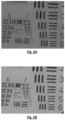
- the invention makes it possible to obtain a representation of a sample, whether it is an acquired image or an image obtained by applying a holographic reconstruction operator to the acquired image, using a simple, inexpensive light source that does not require the interposition of a spatial filter between the sample and the light source.
- the invention may be used for the observation of samples of the biological tissue type, biological particles, or other particles, so as to characterize samples in the fields of health or other industrial applications, for example the environment or the food industry.
Landscapes
- Physics & Mathematics (AREA)
- General Physics & Mathematics (AREA)
- Engineering & Computer Science (AREA)
- Computing Systems (AREA)
- Theoretical Computer Science (AREA)
- Investigating Or Analysing Materials By Optical Means (AREA)
Claims (13)
- Vorrichtung zur Beobachtung einer Probe, umfassend:• einen Träger (10s), der geeignet ist, die Probe (10) aufzunehmen• eine Lichtquelle (11), die geeignet ist, eine einfallende Lichtwelle (12) zu emittieren, die sich zu dem Träger (10s) hin ausbreitet ;• einen Bildsensor (16), der geeignet ist, eine Lichtwelle, die von der Probe durchgelassen wird, wenn die Probe auf dem Träger angeordnet ist, zwischen der Lichtquelle und dem Bildsensor zu detektieren, wobei der Abstand zwischen der Lichtquelle und der Probe dabei größer als 1 cm ist;dadurch gekennzeichnet, dass die Lichtquelle (11) eine sogenannte mikrometrische Leuchtdiode (11i, 11ij) umfasst, bei der eine Lichtemissionsfläche einen Durchmesser oder eine größte Diagonale von weniger als 500 µm aufweist, wobei die mikrometrische Leuchtdiode eine optische Emissionsleistung von mehr als 50 µW aufweist;und dadurch, dass keine Vergrößerungsoptik zwischen der Probe (10), wenn sie auf dem Träger (10s) angeordnet ist, und dem Bildsensor (16) angeordnet ist.
- Vorrichtung zur Beobachtung einer Probe nach Anspruch 1, wobei die Emissionsfläche der mikrometrischen Leuchtdiode (11i, 11ij) einen Durchmesser oder eine größte Diagonale von weniger als 150 µm oder als 100 µm oder 50 µm oder als 10 µm aufweist.
- Vorrichtung nach einem der vorhergehenden Ansprüche, wobei die Lichtquelle (11) eine Mehrzahl von mikrometrischen Leuchtdioden (11i, 11ij) umfasst.
- Vorrichtung nach Anspruch 3, wobei die mikrometrischen Leuchtdioden (11i, 11ij) gemäß einer Matrix angeordnet sind, wobei sie voneinander um einen Abstand von weniger als 50 µm beabstandet sind.
- Vorrichtung nach einem der Ansprüche 3 oder 4, wobei die mikrometrischen Leuchtdioden (11i, 11ij) voneinander verschiedene Emissionsspektralbänder haben und geeignet sind, sukzessive oder gleichzeitig aktiviert zu werden.
- Vorrichtung nach einem der Ansprüche 3 bis 5, wobei die mikrometrischen Leuchtdioden (11i, 11ij) geeignet sind, unabhängig voneinander aktiviert zu werden.
- Verfahren zur Beobachtung einer Probe, umfassend die folgenden Schritte:a) Anordnen einer Probe (10) zwischen einer Lichtquelle (11) und einem Bildsensor (16) derart, dass der Bildsensor geeignet ist, ein Bild der Probe zu erfassen, wenn die Probe durch die Lichtquelle (11) beleuchtet wird, wobei die Lichtquelle in einem Abstand von der Probe von mehr als 1 cm angeordnet ist;b) Beleuchten der Probe durch die Lichtquelle und Erfassen eines Bildes der Probe durch den Bildsensor (16);wobei das Verfahren dadurch gekennzeichnet ist, dass es unter Verwendung einer Lichtquelle (11) durchgeführt wird, die mindestens eine mikrometrische Leuchtdiode (11i, 11ij) umfasst, deren Emissionsfläche einen größten Durchmesser oder eine größte Diagonale von weniger als 500 µm aufweist, die Emissionsleistung der Lichtquelle mehr als 50 µW beträgt, und dadurch, dass keine Vergrößerungsoptik zwischen der Probe (10) und dem Bildsensor (16) angeordnet ist.
- Verfahren zur Beobachtung einer Probe nach Anspruch 7, wobei der größte Durchmesser oder die größte Diagonale der Emissionsfläche der mikrometrischen Leuchtdiode (11i, 11ij) weniger als 150 µm oder als 100 µm oder als 50 µm oder als 10 µm aufweist.
- Verfahren nach einem der Ansprüche 7 oder 8, wobei die Lichtquelle eine Mehrzahl von mikrometrischen Leuchtdioden (11i, 11ij) umfasst.
- Verfahren nach Anspruch 9, wobei die mikrometrischen Leuchtdioden (11i, 11ij) sukzessive aktiviert werden, wobei der Bildsensor bei jeder sukzessiven Aktivierung ein Bild erfasst.
- Verfahren nach einem der Ansprüche 9 oder 10, wobei die mikrometrischen Leuchtdioden voneinander verschiedene Emissionsspektralbänder (Δλ) haben.
- Verfahren nach einem der Ansprüche 7 bis 11, wobei, wenn der Bildsensor (16) sich in einer Detektionsebene (P) erstreckt, das Verfahren ein Anwenden eines Ausbreitungsoperators (h) auf jedes erfasste Bild umfasst, so dass ein komplexer Ausdruck (A) einer Lichtwelle (14), mit welcher der Bildsensor belichtet wird, in einer Rekonstruktionsebene (Pz ) erhalten wird, die in einem Abstand ungleich null von der Detektionsebene gelegen ist.
- Verfahren nach Anspruch 12, wobei die Rekonstruktionsebene eine Ebene ist, entlang der sich die Probe erstreckt.
Applications Claiming Priority (1)
| Application Number | Priority Date | Filing Date | Title |
|---|---|---|---|
| FR1656751A FR3054037B1 (fr) | 2016-07-13 | 2016-07-13 | Dispositif d’observation d’un echantillon |
Publications (2)
| Publication Number | Publication Date |
|---|---|
| EP3270232A1 EP3270232A1 (de) | 2018-01-17 |
| EP3270232B1 true EP3270232B1 (de) | 2025-07-02 |
Family
ID=57121323
Family Applications (1)
| Application Number | Title | Priority Date | Filing Date |
|---|---|---|---|
| EP17180937.9A Active EP3270232B1 (de) | 2016-07-13 | 2017-07-12 | Beobachtungsvorrichtung für eine probe |
Country Status (3)
| Country | Link |
|---|---|
| US (1) | US20180017939A1 (de) |
| EP (1) | EP3270232B1 (de) |
| FR (1) | FR3054037B1 (de) |
Families Citing this family (27)
| Publication number | Priority date | Publication date | Assignee | Title |
|---|---|---|---|---|
| US11961875B2 (en) | 2017-12-20 | 2024-04-16 | Lumileds Llc | Monolithic segmented LED array architecture with islanded epitaxial growth |
| US20190198564A1 (en) | 2017-12-20 | 2019-06-27 | Lumileds Llc | Monolithic segmented led array architecture with islanded epitaxial growth |
| US11201265B2 (en) | 2018-09-27 | 2021-12-14 | Lumileds Llc | Micro light emitting devices |
| FR3087538B1 (fr) * | 2018-10-17 | 2020-10-09 | Commissariat Energie Atomique | Procede d'observation d'un echantillon |
| FR3094988A1 (fr) | 2019-04-12 | 2020-10-16 | Commissariat à l'Energie Atomique et aux Energies Alternatives | Procédé d'observation précoce de colonies de microorganismes |
| US11777059B2 (en) | 2019-11-20 | 2023-10-03 | Lumileds Llc | Pixelated light-emitting diode for self-aligned photoresist patterning |
| US11674795B2 (en) | 2019-12-18 | 2023-06-13 | Lumileds Llc | Miniature pattern projector using microLEDs and micro-optics |
| US11569415B2 (en) | 2020-03-11 | 2023-01-31 | Lumileds Llc | Light emitting diode devices with defined hard mask opening |
| US11735695B2 (en) | 2020-03-11 | 2023-08-22 | Lumileds Llc | Light emitting diode devices with current spreading layer |
| US11942507B2 (en) | 2020-03-11 | 2024-03-26 | Lumileds Llc | Light emitting diode devices |
| US11848402B2 (en) | 2020-03-11 | 2023-12-19 | Lumileds Llc | Light emitting diode devices with multilayer composite film including current spreading layer |
| US11626538B2 (en) | 2020-10-29 | 2023-04-11 | Lumileds Llc | Light emitting diode device with tunable emission |
| US11901491B2 (en) | 2020-10-29 | 2024-02-13 | Lumileds Llc | Light emitting diode devices |
| US12040432B2 (en) | 2020-10-30 | 2024-07-16 | Lumileds Llc | Light emitting diode devices with patterned TCO layer including different thicknesses |
| US11705534B2 (en) | 2020-12-01 | 2023-07-18 | Lumileds Llc | Methods of making flip chip micro light emitting diodes |
| US11955583B2 (en) | 2020-12-01 | 2024-04-09 | Lumileds Llc | Flip chip micro light emitting diodes |
| US11600656B2 (en) | 2020-12-14 | 2023-03-07 | Lumileds Llc | Light emitting diode device |
| US12484346B2 (en) | 2021-09-03 | 2025-11-25 | Lumileds Singapore Pte. Ltd. | Light emitting diode devices with bonding and/or ohmic contact-reflective material |
| US12402440B2 (en) | 2021-09-03 | 2025-08-26 | Lumileds Llc | Light emitting diode devices with bonding and/or ohmic contact-reflective material |
| US12419137B2 (en) | 2021-09-10 | 2025-09-16 | Lumileds Llc | Light emitting diodes with segmented anodes by pixel |
| US12433080B2 (en) | 2021-09-29 | 2025-09-30 | Lumileds Singapore Pte. Ltd. | Hybrid CMOS micro-LED display layout |
| US12431478B2 (en) | 2021-09-29 | 2025-09-30 | Lumileds Singapore Pte. Ltd. | Hybrid CMOS micro-LED display layout |
| US12568728B2 (en) | 2021-09-29 | 2026-03-03 | Lumileds Singapore Pte. Ltd. | Hybrid CMOS micro-LED display layout |
| US11935987B2 (en) | 2021-11-03 | 2024-03-19 | Lumileds Llc | Light emitting diode arrays with a light-emitting pixel area |
| US12490570B2 (en) | 2021-11-12 | 2025-12-02 | Lumileds Singapore Pte. Ltd. | Thin-film LED array with low refractive index patterned structures |
| US12588326B2 (en) | 2021-11-12 | 2026-03-24 | Lumileds Singapore Pte. Ltd. | Composite cathode contact for monolithically integrated micro-LEDs, mini-LEDs and LED arrays |
| US12604572B2 (en) | 2021-11-12 | 2026-04-14 | Lumileds Singapore Pte. Ltd. | Thin-film LED array with low refractive index patterned structures and reflector |
Citations (2)
| Publication number | Priority date | Publication date | Assignee | Title |
|---|---|---|---|---|
| WO2017162985A1 (fr) * | 2016-03-23 | 2017-09-28 | Commissariat à l'énergie atomique et aux énergies alternatives | Procédé d'observation d'un échantillon par calcul d'une image complexe |
| WO2017178723A1 (fr) * | 2016-03-23 | 2017-10-19 | Commissariat à l'énergie atomique et aux énergies alternatives | Procédé de caractérisation holographique d'une particule dans un échantillon |
Family Cites Families (3)
| Publication number | Priority date | Publication date | Assignee | Title |
|---|---|---|---|---|
| CA2645104A1 (en) * | 2006-03-09 | 2007-09-13 | Tessarae, Llc | Microarray imaging system and associated methodology |
| GB0701201D0 (en) * | 2007-01-22 | 2007-02-28 | Cancer Rec Tech Ltd | Cell mapping and tracking |
| FR3002634B1 (fr) * | 2013-02-28 | 2015-04-10 | Commissariat Energie Atomique | Procede d'observation d'au moins un objet, tel qu'une entite biologique, et systeme d'imagerie associe |
-
2016
- 2016-07-13 FR FR1656751A patent/FR3054037B1/fr active Active
-
2017
- 2017-07-12 EP EP17180937.9A patent/EP3270232B1/de active Active
- 2017-07-13 US US15/648,996 patent/US20180017939A1/en not_active Abandoned
Patent Citations (5)
| Publication number | Priority date | Publication date | Assignee | Title |
|---|---|---|---|---|
| WO2017162985A1 (fr) * | 2016-03-23 | 2017-09-28 | Commissariat à l'énergie atomique et aux énergies alternatives | Procédé d'observation d'un échantillon par calcul d'une image complexe |
| WO2017178723A1 (fr) * | 2016-03-23 | 2017-10-19 | Commissariat à l'énergie atomique et aux énergies alternatives | Procédé de caractérisation holographique d'une particule dans un échantillon |
| EP3433679A1 (de) * | 2016-03-23 | 2019-01-30 | Commissariat à l'Énergie Atomique et aux Énergies Alternatives | Verfahren zur beobachtung einer probe durch berechnung eines komplexen bildes |
| EP3433678A1 (de) * | 2016-03-23 | 2019-01-30 | Commissariat à l'Energie Atomique et aux Energies Alternatives | Holographisches verfahren zur charakterisierung eines partikels in einer probe |
| EP3433679B1 (de) * | 2016-03-23 | 2020-11-04 | Commissariat à l'Énergie Atomique et aux Énergies Alternatives | Verfahren zur beobachtung einer probe durch berechnung eines komplexen bildes |
Also Published As
| Publication number | Publication date |
|---|---|
| FR3054037A1 (fr) | 2018-01-19 |
| EP3270232A1 (de) | 2018-01-17 |
| FR3054037B1 (fr) | 2018-08-17 |
| US20180017939A1 (en) | 2018-01-18 |
Similar Documents
| Publication | Publication Date | Title |
|---|---|---|
| EP3270232B1 (de) | Beobachtungsvorrichtung für eine probe | |
| EP3433679B1 (de) | Verfahren zur beobachtung einer probe durch berechnung eines komplexen bildes | |
| EP3274689B1 (de) | Verfahren und vorrichtung zur analyse von partikeln | |
| EP3274694B1 (de) | Verfahren zur bestimmung des zustandes einer zelle | |
| WO2016189257A1 (fr) | Procédé d'observation d'un échantillon | |
| FR3049348A1 (fr) | Procede de caracterisation d’une particule dans un echantillon | |
| EP3519899B1 (de) | Vorrichtung zur beobachtung einer probe und verfahren zur beobachtung einer probe | |
| EP3394591B1 (de) | Beobachtungsverfahren einer probe in einer linsenlosen abbildung | |
| FR3060746A1 (fr) | Procede de numeration de particules dans un echantillon par imagerie sans lentille | |
| EP2556164A1 (de) | Verfahren für den nachweis von clustern aus biologischen partikeln | |
| EP3397944B1 (de) | Vorrichtung und verfahren zur bimodalen beobachtung eines objekts | |
| FR3047077A1 (fr) | Procede d’observation d’un echantillon par imagerie sans lentille | |
| FR3026836A1 (fr) | Methode et dispositif optique de telemetrie | |
| EP4260116B1 (de) | Konfokales mikroskop mit photonen-umverteilung | |
| FR3087009A1 (fr) | Procede de determination de parametres d'une particule | |
| FR2993372A1 (fr) | Procede et systeme de reconstruction de proprietes optiques d'objets diffractants baignant dans un milieu liquide | |
| EP3371574B1 (de) | Vorrichtung und verfahren zur beobachtung eines objekts mittels linsenfreier abbildung | |
| EP4020093B1 (de) | Verfahren zur erzeugung eines komplexen bildes einer probe | |
| EP3545362B1 (de) | Verfahren zur herstellung eines hochauflösenden bildes durch linsenlose bildgebung | |
| EP1579260A1 (de) | Paralleles konfokales lasermikroskopiesystem auf der basis von vcsel-technologie | |
| WO2015132360A1 (fr) | Procédé et système de caractérisation d'un état d'adhésion de particules, telles que des cellules | |
| FR3082943A1 (fr) | Procede de comptage de particules de petite taille dans un echantillon | |
| EP3221689B1 (de) | Verfahren zur beobachtung mehrerer proben und zugehörige vorrichtung | |
| WO2025099033A1 (fr) | Appareil et procédé de micro-spectrométrie raman confocal avec système de mise au point | |
| FR3086758A1 (fr) | Procede et dispositif d'observation d'un echantillon sous lumiere ambiante |
Legal Events
| Date | Code | Title | Description |
|---|---|---|---|
| PUAI | Public reference made under article 153(3) epc to a published international application that has entered the european phase |
Free format text: ORIGINAL CODE: 0009012 |
|
| STAA | Information on the status of an ep patent application or granted ep patent |
Free format text: STATUS: REQUEST FOR EXAMINATION WAS MADE |
|
| 17P | Request for examination filed |
Effective date: 20170712 |
|
| AK | Designated contracting states |
Kind code of ref document: A1 Designated state(s): AL AT BE BG CH CY CZ DE DK EE ES FI FR GB GR HR HU IE IS IT LI LT LU LV MC MK MT NL NO PL PT RO RS SE SI SK SM TR |
|
| AX | Request for extension of the european patent |
Extension state: BA ME |
|
| STAA | Information on the status of an ep patent application or granted ep patent |
Free format text: STATUS: EXAMINATION IS IN PROGRESS |
|
| 17Q | First examination report despatched |
Effective date: 20210422 |
|
| RAP3 | Party data changed (applicant data changed or rights of an application transferred) |
Owner name: COMMISSARIAT A L'ENERGIE ATOMIQUE ET AUX ENERGIESALTERNATIVES |
|
| GRAP | Despatch of communication of intention to grant a patent |
Free format text: ORIGINAL CODE: EPIDOSNIGR1 |
|
| STAA | Information on the status of an ep patent application or granted ep patent |
Free format text: STATUS: GRANT OF PATENT IS INTENDED |
|
| INTG | Intention to grant announced |
Effective date: 20250128 |
|
| GRAS | Grant fee paid |
Free format text: ORIGINAL CODE: EPIDOSNIGR3 |
|
| GRAA | (expected) grant |
Free format text: ORIGINAL CODE: 0009210 |
|
| STAA | Information on the status of an ep patent application or granted ep patent |
Free format text: STATUS: THE PATENT HAS BEEN GRANTED |
|
| AK | Designated contracting states |
Kind code of ref document: B1 Designated state(s): AL AT BE BG CH CY CZ DE DK EE ES FI FR GB GR HR HU IE IS IT LI LT LU LV MC MK MT NL NO PL PT RO RS SE SI SK SM TR |
|
| REG | Reference to a national code |
Ref country code: GB Ref legal event code: FG4D Free format text: NOT ENGLISH |
|
| REG | Reference to a national code |
Ref country code: CH Ref legal event code: EP |
|
| REG | Reference to a national code |
Ref country code: DE Ref legal event code: R096 Ref document number: 602017090237 Country of ref document: DE |
|
| REG | Reference to a national code |
Ref country code: IE Ref legal event code: FG4D Free format text: LANGUAGE OF EP DOCUMENT: FRENCH |
|
| PGFP | Annual fee paid to national office [announced via postgrant information from national office to epo] |
Ref country code: DE Payment date: 20250826 Year of fee payment: 9 |
|
| PGFP | Annual fee paid to national office [announced via postgrant information from national office to epo] |
Ref country code: GB Payment date: 20250828 Year of fee payment: 9 |
|
| PGFP | Annual fee paid to national office [announced via postgrant information from national office to epo] |
Ref country code: FR Payment date: 20250828 Year of fee payment: 9 |
|
| REG | Reference to a national code |
Ref country code: NL Ref legal event code: MP Effective date: 20250702 |
|
| PG25 | Lapsed in a contracting state [announced via postgrant information from national office to epo] |
Ref country code: PT Free format text: LAPSE BECAUSE OF FAILURE TO SUBMIT A TRANSLATION OF THE DESCRIPTION OR TO PAY THE FEE WITHIN THE PRESCRIBED TIME-LIMIT Effective date: 20251103 |
|
| PG25 | Lapsed in a contracting state [announced via postgrant information from national office to epo] |
Ref country code: NL Free format text: LAPSE BECAUSE OF FAILURE TO SUBMIT A TRANSLATION OF THE DESCRIPTION OR TO PAY THE FEE WITHIN THE PRESCRIBED TIME-LIMIT Effective date: 20250702 |
|
| REG | Reference to a national code |
Ref country code: AT Ref legal event code: MK05 Ref document number: 1809909 Country of ref document: AT Kind code of ref document: T Effective date: 20250702 |
|
| PG25 | Lapsed in a contracting state [announced via postgrant information from national office to epo] |
Ref country code: IS Free format text: LAPSE BECAUSE OF FAILURE TO SUBMIT A TRANSLATION OF THE DESCRIPTION OR TO PAY THE FEE WITHIN THE PRESCRIBED TIME-LIMIT Effective date: 20251102 |
|
| PG25 | Lapsed in a contracting state [announced via postgrant information from national office to epo] |
Ref country code: NO Free format text: LAPSE BECAUSE OF FAILURE TO SUBMIT A TRANSLATION OF THE DESCRIPTION OR TO PAY THE FEE WITHIN THE PRESCRIBED TIME-LIMIT Effective date: 20251002 |
|
| REG | Reference to a national code |
Ref country code: LT Ref legal event code: MG9D |
|
| PG25 | Lapsed in a contracting state [announced via postgrant information from national office to epo] |
Ref country code: AT Free format text: LAPSE BECAUSE OF FAILURE TO SUBMIT A TRANSLATION OF THE DESCRIPTION OR TO PAY THE FEE WITHIN THE PRESCRIBED TIME-LIMIT Effective date: 20250702 |
|
| PG25 | Lapsed in a contracting state [announced via postgrant information from national office to epo] |
Ref country code: FI Free format text: LAPSE BECAUSE OF FAILURE TO SUBMIT A TRANSLATION OF THE DESCRIPTION OR TO PAY THE FEE WITHIN THE PRESCRIBED TIME-LIMIT Effective date: 20250702 |
|
| PG25 | Lapsed in a contracting state [announced via postgrant information from national office to epo] |
Ref country code: HR Free format text: LAPSE BECAUSE OF FAILURE TO SUBMIT A TRANSLATION OF THE DESCRIPTION OR TO PAY THE FEE WITHIN THE PRESCRIBED TIME-LIMIT Effective date: 20250702 |
|
| PG25 | Lapsed in a contracting state [announced via postgrant information from national office to epo] |
Ref country code: GR Free format text: LAPSE BECAUSE OF FAILURE TO SUBMIT A TRANSLATION OF THE DESCRIPTION OR TO PAY THE FEE WITHIN THE PRESCRIBED TIME-LIMIT Effective date: 20251003 |
|
| PG25 | Lapsed in a contracting state [announced via postgrant information from national office to epo] |
Ref country code: CZ Free format text: LAPSE BECAUSE OF FAILURE TO SUBMIT A TRANSLATION OF THE DESCRIPTION OR TO PAY THE FEE WITHIN THE PRESCRIBED TIME-LIMIT Effective date: 20250702 Ref country code: SE Free format text: LAPSE BECAUSE OF FAILURE TO SUBMIT A TRANSLATION OF THE DESCRIPTION OR TO PAY THE FEE WITHIN THE PRESCRIBED TIME-LIMIT Effective date: 20250702 |
|
| PG25 | Lapsed in a contracting state [announced via postgrant information from national office to epo] |
Ref country code: LV Free format text: LAPSE BECAUSE OF FAILURE TO SUBMIT A TRANSLATION OF THE DESCRIPTION OR TO PAY THE FEE WITHIN THE PRESCRIBED TIME-LIMIT Effective date: 20250702 |
|
| PG25 | Lapsed in a contracting state [announced via postgrant information from national office to epo] |
Ref country code: BG Free format text: LAPSE BECAUSE OF FAILURE TO SUBMIT A TRANSLATION OF THE DESCRIPTION OR TO PAY THE FEE WITHIN THE PRESCRIBED TIME-LIMIT Effective date: 20250702 Ref country code: PL Free format text: LAPSE BECAUSE OF FAILURE TO SUBMIT A TRANSLATION OF THE DESCRIPTION OR TO PAY THE FEE WITHIN THE PRESCRIBED TIME-LIMIT Effective date: 20250702 |
|
| PG25 | Lapsed in a contracting state [announced via postgrant information from national office to epo] |
Ref country code: RS Free format text: LAPSE BECAUSE OF FAILURE TO SUBMIT A TRANSLATION OF THE DESCRIPTION OR TO PAY THE FEE WITHIN THE PRESCRIBED TIME-LIMIT Effective date: 20251002 |
|
| PG25 | Lapsed in a contracting state [announced via postgrant information from national office to epo] |
Ref country code: ES Free format text: LAPSE BECAUSE OF FAILURE TO SUBMIT A TRANSLATION OF THE DESCRIPTION OR TO PAY THE FEE WITHIN THE PRESCRIBED TIME-LIMIT Effective date: 20250702 |
|
| REG | Reference to a national code |
Ref country code: CH Ref legal event code: H13 Free format text: ST27 STATUS EVENT CODE: U-0-0-H10-H13 (AS PROVIDED BY THE NATIONAL OFFICE) Effective date: 20260224 |
|
| PG25 | Lapsed in a contracting state [announced via postgrant information from national office to epo] |
Ref country code: LU Free format text: LAPSE BECAUSE OF NON-PAYMENT OF DUE FEES Effective date: 20250712 Ref country code: RO Free format text: LAPSE BECAUSE OF FAILURE TO SUBMIT A TRANSLATION OF THE DESCRIPTION OR TO PAY THE FEE WITHIN THE PRESCRIBED TIME-LIMIT Effective date: 20250702 |
|
| REG | Reference to a national code |
Ref country code: BE Ref legal event code: MM Effective date: 20250731 |
|
| PG25 | Lapsed in a contracting state [announced via postgrant information from national office to epo] |
Ref country code: SM Free format text: LAPSE BECAUSE OF FAILURE TO SUBMIT A TRANSLATION OF THE DESCRIPTION OR TO PAY THE FEE WITHIN THE PRESCRIBED TIME-LIMIT Effective date: 20250702 |
|
| PG25 | Lapsed in a contracting state [announced via postgrant information from national office to epo] |
Ref country code: DK Free format text: LAPSE BECAUSE OF FAILURE TO SUBMIT A TRANSLATION OF THE DESCRIPTION OR TO PAY THE FEE WITHIN THE PRESCRIBED TIME-LIMIT Effective date: 20250702 |
|
| PG25 | Lapsed in a contracting state [announced via postgrant information from national office to epo] |
Ref country code: BE Free format text: LAPSE BECAUSE OF NON-PAYMENT OF DUE FEES Effective date: 20250731 Ref country code: IT Free format text: LAPSE BECAUSE OF FAILURE TO SUBMIT A TRANSLATION OF THE DESCRIPTION OR TO PAY THE FEE WITHIN THE PRESCRIBED TIME-LIMIT Effective date: 20250702 |
|
| PG25 | Lapsed in a contracting state [announced via postgrant information from national office to epo] |
Ref country code: CH Free format text: LAPSE BECAUSE OF NON-PAYMENT OF DUE FEES Effective date: 20250731 |
|
| PG25 | Lapsed in a contracting state [announced via postgrant information from national office to epo] |
Ref country code: SK Free format text: LAPSE BECAUSE OF FAILURE TO SUBMIT A TRANSLATION OF THE DESCRIPTION OR TO PAY THE FEE WITHIN THE PRESCRIBED TIME-LIMIT Effective date: 20250702 Ref country code: EE Free format text: LAPSE BECAUSE OF FAILURE TO SUBMIT A TRANSLATION OF THE DESCRIPTION OR TO PAY THE FEE WITHIN THE PRESCRIBED TIME-LIMIT Effective date: 20250702 |