EP3273601A1 - Convertisseur temps-numérique et boucle numérique à verrouillage de phase - Google Patents
Convertisseur temps-numérique et boucle numérique à verrouillage de phase Download PDFInfo
- Publication number
- EP3273601A1 EP3273601A1 EP16856464.9A EP16856464A EP3273601A1 EP 3273601 A1 EP3273601 A1 EP 3273601A1 EP 16856464 A EP16856464 A EP 16856464A EP 3273601 A1 EP3273601 A1 EP 3273601A1
- Authority
- EP
- European Patent Office
- Prior art keywords
- stage
- time
- converting circuit
- delayer
- digital converter
- Prior art date
- Legal status (The legal status is an assumption and is not a legal conclusion. Google has not performed a legal analysis and makes no representation as to the accuracy of the status listed.)
- Ceased
Links
Images


Classifications
-
- H—ELECTRICITY
- H03—ELECTRONIC CIRCUITRY
- H03M—CODING; DECODING; CODE CONVERSION IN GENERAL
- H03M1/00—Analogue/digital conversion; Digital/analogue conversion
- H03M1/002—Provisions or arrangements for saving power, e.g. by allowing a sleep mode, using lower supply voltage for downstream stages, using multiple clock domains or by selectively turning on stages when needed
-
- G—PHYSICS
- G04—HOROLOGY
- G04F—TIME-INTERVAL MEASURING
- G04F10/00—Apparatus for measuring unknown time intervals by electric means
- G04F10/005—Time-to-digital converters [TDC]
-
- H—ELECTRICITY
- H03—ELECTRONIC CIRCUITRY
- H03L—AUTOMATIC CONTROL, STARTING, SYNCHRONISATION OR STABILISATION OF GENERATORS OF ELECTRONIC OSCILLATIONS OR PULSES
- H03L7/00—Automatic control of frequency or phase; Synchronisation
- H03L7/06—Automatic control of frequency or phase; Synchronisation using a reference signal applied to a frequency- or phase-locked loop
- H03L7/08—Details of the phase-locked loop
- H03L7/081—Details of the phase-locked loop provided with an additional controlled phase shifter
- H03L7/0812—Details of the phase-locked loop provided with an additional controlled phase shifter and where no voltage or current controlled oscillator is used
- H03L7/0814—Details of the phase-locked loop provided with an additional controlled phase shifter and where no voltage or current controlled oscillator is used the phase shifting device being digitally controlled
-
- H—ELECTRICITY
- H03—ELECTRONIC CIRCUITRY
- H03M—CODING; DECODING; CODE CONVERSION IN GENERAL
- H03M1/00—Analogue/digital conversion; Digital/analogue conversion
- H03M1/12—Analogue/digital converters
- H03M1/1205—Multiplexed conversion systems
-
- H—ELECTRICITY
- H03—ELECTRONIC CIRCUITRY
- H03M—CODING; DECODING; CODE CONVERSION IN GENERAL
- H03M1/00—Analogue/digital conversion; Digital/analogue conversion
- H03M1/12—Analogue/digital converters
- H03M1/50—Analogue/digital converters with intermediate conversion to time interval
- H03M1/502—Analogue/digital converters with intermediate conversion to time interval using tapped delay lines
-
- H—ELECTRICITY
- H03—ELECTRONIC CIRCUITRY
- H03L—AUTOMATIC CONTROL, STARTING, SYNCHRONISATION OR STABILISATION OF GENERATORS OF ELECTRONIC OSCILLATIONS OR PULSES
- H03L2207/00—Indexing scheme relating to automatic control of frequency or phase and to synchronisation
- H03L2207/50—All digital phase-locked loop
Definitions
- This application relates to the field of circuit technologies, and in particular, to a time-to-digital converter and a digital phase locked loop.
- a time-to-digital converter implements conversion from time signals to digital signals by sampling and quantizing time intervals.
- the time-to-digital converter is widely used in such fields as space exploration, high energy physics, and test equipment, and in recent years, the time-to-digital converter is greatly promoted as a key module in a digital phase locked loop (DPLL).
- DPLL digital phase locked loop
- a structure of a time-to-digital converter in a digital phase locked loop includes a reference clock signal input end and a sampling clock signal input end. After a reference clock signal is input, the reference clock signal passes through multiple stages of same delayers. When a first stage of delayer is passed through, a delayed signal having a delay duration of t is output (t is a degree of precision of the time-to-digital converter), and the delayed signal that is output by the first stage of delayer is input to a second stage of delayer, to obtain a delayed signal having a delay duration of two times of t.
- a delayed signal obtained by an (i-1) th stage of delayer is input to an i th stage of delayer, to obtain a delayed signal having a delay duration of i times of t.
- a sampling clock signal separately samples the series of obtained delayed signals, to obtain a series of output signals.
- a dynamic range of the time-to-digital converter is t ⁇ i, and if t remains unchanged and the time-to-digital converter needs to obtain a large dynamic range, a quantity of stages of delayers needs to be increased.
- an increase in the quantity of stages of delayers directly results in an increase in a quantity of stages of the time-to-digital converter, and the area and power consumption of the time-to-digital converter both increase accordingly.
- This application provides a time-to-digital converter and a digital phase locked loop, to reduce the area and power consumption of a time-to-digital converter while maintaining a dynamic range of the time-to-digital converter.
- an embodiment of the present invention provides a time-to-digital converter, including N stages of converting circuits connected in series, where N ⁇ 2, and N is an integer; each stage of converting circuit includes a first delayer and an arbiter, where a first delayer in a first stage of converting circuit is configured to receive a reference signal, an input end of the first delayer in each stage of converting circuit other than the first stage of converting circuit is coupled to an output end of a first delayer in a previous stage of converting circuit, and an output end of the first delayer in each stage of converting circuit is configured to output a delayed signal of the stage of converting circuit; and the arbiter in each stage of converting circuit is configured to: receive a sampling clock of the stage of converting circuit and the delayed signal of the stage of converting circuit, and compare the sampling clock with the delayed signal to obtain an output signal of the stage of converting circuit, where the sampling clock of each stage of converting circuit is derived from a clock signal; in the N stages of
- the first delayer in each stage of converting circuit includes at least one first delay cell circuit; and quantities of first delay cell circuits included in first delayers in the at least two stages of converting circuits are different.
- the sampling clock of each stage of converting circuit is the clock signal.
- each stage of converting circuit further includes a second delayer, where a second delayer in the first stage of converting circuit is configured to receive the clock signal, an input end of the second delayer in each stage of converting circuit other than the first stage of converting circuit is coupled to an output end of a second delayer in the previous stage of converting circuit, and an output end of the second delayer in each stage of converting circuit is configured to output the sampling clock of the stage of converting circuit.
- a second delay time of the second delayer in each stage of converting circuit is less than a first delay time of the first delayer in the stage of converting circuit.
- the first delayer in each stage of converting circuit includes at least one first delay cell circuit
- the second delayer in the stage of converting circuit includes at least one second delay cell circuit
- a quantity of second delay cell circuits in the second delayer in each stage of converting circuit is equal to a quantity of first delay cell circuits in the first delayer in the stage of converting circuit
- quantities of first delay cell circuits included in first delayers in the at least two stages of converting circuits are different.
- a third delay time of the second delay cell circuit in the second delayer in each stage of converting circuit is less than a fourth delay time of the first delay cell circuit in the first delayer in the stage of converting circuit.
- each stage of converting circuit further includes a synchronization flip-flop; and the synchronization flip-flop in each stage of converting circuit is configured to sample an output signal generated in the stage of converting circuit to synchronize the output signals of the N stages of converting circuits.
- an arbiter in at least one stage of converting circuit is an arbiter or a flip-flop.
- the flip-flop is a D flip-flop.
- a delay time of the first delayer in each stage of converting circuit is not less than a delay time of the first delayer in the previous stage of converting circuit.
- the reference signal is another clock signal.
- the binary number is thermometer code.
- an embodiment of the present invention further provides a digital phase locked loop, including the time-to-digital converter according to any one of the first aspect or the first to the thirteenth possible implementation manners of the first aspect, where the reference signal is a reference clock signal of the digital phase locked loop, and the clock signal is a frequency division signal of an output signal of the digital phase locked loop.
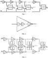
- FIG. 1 is a schematic structural diagram of a time-to-digital converter.
- the time-to-digital converter includes N stages of converting circuits, where N ⁇ 2, and N is an integer.
- a first delayer in a first stage of converting circuit is configured to receive a reference signal ref, an input end of a first delayer in each stage of converting circuit other than the first stage of converting circuit is coupled to an output end of a first delayer in a previous stage of converting circuit, an output end of the first delayer in each stage of converting circuit is configured to output a delayed signal of the stage of converting circuit, and the reference signal may be a clock.
- An arbiter in each stage of converting circuit is configured to: receive a sampling clock of the stage of converting circuit and the delayed signal of the stage of converting circuit, and compare the sampling clock with the delayed signal to obtain an output signal of the stage of converting circuit.
- the arbiter may include a comparator or a flip-flop (Flip-Flop), configured to compare input signals of a second input end and a third input end.
- a common form of the flip-flop is a D flip-flop.
- the sampling clock of each stage of converting circuit is derived from a clock signal clk.
- the comparator and the flip-flop both can implement a function of comparison.
- output signals Q1 to Qn of the time-to-digital converter are a non-linear binary number formed by output signals of the N stages of converting circuits.
- the binary number is used to indicate a time difference between the clock signal and the reference signal, and Q1 to Qn may be specifically thermometer code.
- a degree of indication precision of an output signal corresponding to each stage of converting circuit in the binary number depends on a delay time of the first delayer in the stage of converting circuit.
- the delayer in the time-to-digital converter is provided with a preset quantity of first delay cell circuits, and delay times t1 of all first delay cell circuit are the same. It is assumed that the delay time t1 of the first delay cell circuit is a time unit.
- the first delayer in each stage of converting circuit includes at least one first delay cell circuit, and if a same delayer includes multiple first delay cell circuits, the multiple first delay cell circuits are connected in series; and quantities of first delay cell circuits included in first delayers in the at least two stages of converting circuits are different.
- the delay time t1 of the first delay cell circuit may be set to 20 ps
- a quantity of circuit stages of the time-to-digital converter may be set to 7
- quantities of first delay cell circuits disposed in a series of first delayers corresponding to the first stage to the seventh stage of converting circuits are respectively 1, 1, 2, 4, 8, 16, and 32.
- Corresponding delays of the series of first delayers are respectively 2 0 t1, 2 1 t1, 2 2 t1, 2 3 t1, 2 4 t1, 2 5 t1, and 2 6 t1, which implements outputs of code words in the power of 2.
- correspondingly-output delayed signals of a series of first clocks are delayed 20 ps, 40 ps, 120 ps...640 ps, and 1280 ps correspondingly.
- the time-to-digital converter For a code word of a higher bit, such as Q7, although compared with a time interval between two clock signals obtained by a conventional time-to-digital converter, there is a greater error in the time interval, that is, a lower degree of precision indicates a larger time interval corresponding to the code word, the area and power consumption of the time-to-digital converter both are reduced compared with those of a commonly-used time-to-digital converter.
- the time-to-digital converter provided in this embodiment can also ensure precision within a short input interval.
- the quantity of first delay cell circuits used in the time-to-digital converter in this embodiment is the same as a quantity of delayers in a commonly-used time-to-digital converter, only seven stages of converting circuits are needed, and only seven arbiters are needed correspondingly, so that a quantity of arbiters is reduced, and the area and power consumption of the time-to-digital converter are effectively reduced.
- the time interval between the reference signal ref and the clock signal clk is still 1270 ps.
- a degree of precision of a time-to-digital converter is adjusted to 10 ps in this case, for a commonly-used time-to-digital converter, a delay time of each delayer is 10 ps, and 128 stages of converting circuits are needed. It may be known that in this case, 128 arbiters need to be disposed in the time-to-digital converter, and the area and power consumption of the circuit are excessively large correspondingly. If the time-to-digital converter in FIG.
- the delay time t1 of the delay cell circuit is set to 10 ps
- eight stages of converting circuits are disposed in the time-to-digital converter
- quantities of first delay cell circuits disposed in a series of corresponding first delayers are respectively 1, 1, 2, 4, 8, 16, 32, and 64.
- Corresponding delays of the series of first delayers are respectively 2 0 t1, 2 1 t1, 2 2 t1, 2 3 t1, 2 4 t1, 2 5 t1, 2 6 t1, and 2 7 t1.
- output digital signals Q1 to Q8 are 11111110, it may be determined that a time interval between two clock signals ranges from 640 ps and 1280 ps, and it may be seen that as the degree of precision of the time-to-digital converter increases, the time-to-digital converter provided in this embodiment can reduce a quantity of circuit stages while ensuring a dynamic range of the time-to-digital converter to a greatest extent, thereby reducing the area and power consumption of the time-to-digital converter.
- the time-to-digital converter can still determine a time interval between two signals while ensuring a dynamic range of the time-to-digital converter to a greatest extent, and a quantity of stages of the time-to-digital converter and a quantity of delay cell circuits in each delayer can be flexibly set according to a specific time interval between the two signals.
- the quantity of stages of converting circuits of the time-to-digital converter and the quantity of first delay cell circuits in each delayer above are merely set as examples, and may be designed specifically according to an actual case.
- the quantity of stages of converting circuits may be increased or reduced, and sequentially delayed signals of the reference signal ref may be a square or a cube of a natural number, or another irregular relationship may be used.
- quantities of first delay cell circuits disposed in a series of first delayers are respectively 1, 3, 5, 7..., and accumulated delays of outputs corresponding to stages are 1, 4, 9, 16....
- an embodiment provides a time-to-digital converter, including N stages of converting circuits, where N ⁇ 2, and N is an integer.
- Each stage of converting circuit includes a first delayer and an arbiter.
- the first delayer in the converting circuit is provided with a preset quantity of first delay cell circuits, and quantities of first delay cell circuits included in first delayers in at least two stages of converting circuits are different.
- the N stages of converting circuits each have a same first delay cell circuit, a stable delay ratio and a precise delay time of each stage of converting circuit are ensured, and the quantity of first delay cell circuits in each first delayer may be preset as required, so that in a case of a large dynamic range, a quantity of circuit stages can be effectively reduced, thereby reducing the area and power consumption of a circuit.
- a degree of precision of the time-to-digital converter is limited by the first delay cell circuit, and a minimum degree of precision is a delay of one first delay cell circuit.
- FIG. 3 is a schematic structural diagram of another time-to-digital converter according to an embodiment of the present invention. Different from the time-to-digital converter provided in FIG. 1 , in this time-to-digital converter, each stage of converting circuit further includes a second delayer.
- a second delayer in the first stage of converting circuit is configured to receive the clock signal clk, an input end of the second delayer in each stage of converting circuit other than the first stage of converting circuit is coupled to an output end of a second delayer in a previous stage of converting circuit, and an output end of the second delayer in each stage of converting circuit is configured to output a sampling clock of the stage of converting circuit.
- the second delayer is provided with a preset quantity of second delay cell circuits, and the second delay cell circuits are connected in series.
- a second delay time of the second delayer in each stage of converting circuit is less than a first delay time of the first delayer in the stage of converting circuit.
- a binary number that is output by output signals Q1 to Qn of the time-to-digital converter provided in this embodiment and a degree of indication precision of an output signal corresponding to each stage of converting circuit depend on a difference between a delay time of the first delayer and a delay time of the second delayer in the stage of converting circuit.
- a quantity of second delay cell circuits is equal to a quantity of first delay cell circuits in a same stage of converting circuit, and it needs to be ensured that a third delay time of the second delay cell circuit is less than a fourth delay time of the first delay cell circuit.
- t1 is the fourth delay time of the first delay cell circuit
- t2 is the third delay time of the second delay cell circuit.
- the first delayer in the first stage of converting circuit is provided with one first delay cell circuit
- a second delayer in the corresponding stage of converting circuit is also provided with one second delay cell circuit.
- First delayers in remaining N-1 stages of converting circuits are respectively provided with n1, n2...nx first delay cell circuits
- a quantity of second delay cell circuits disposed in a second delayer in a corresponding stage of converting circuit is the same as a quantity of first delay cell circuits disposed in the first delayer in the stage of converting circuit.
- a synchronization flip-flop may be added behind the arbiter or flip-flop. Therefore, the arbiter configured to compare two signals in the embodiment corresponding to FIG. 3 may include either one of a comparator or a flip-flop, and the synchronization flip-flop. Each stage of synchronization flip-flop samples output of each stage of arbiter by using a synchronization clock, to ensure synchronization of each stage of output signal.
- the synchronization flip-flop and the arbiter are similar flip-flops, and may be simple D flip-flops or flip-flops in another architecture.
- a time interval between two clock signals is still 1270 ps.
- a degree of precision of a time-to-digital converter is 20 ps
- a conventional time-to-digital converter needs 64 stages of converting circuits, and the time-to-digital converter provided in FIG. 1 needs only seven stages of converting circuits, but a problem occurs in the time-to-digital converter provided in FIG. 1 is that a minimum degree of precision is a delay time of one first delay cell circuit.
- a minimum degree of precision is a delay time of one first delay cell circuit.
- a second delay cell circuit is introduced, and that the time-to-digital converter needs only seven stages of converting circuits is also ensured, but a degree of precision of the time-to-digital converter is t1-t2.
- t1 and t2 may have any values, as long as t1 is greater than t2. Therefore, the time-to-digital converter in this embodiment may obtain more flexible precision.
- each stage of converting circuit includes same quantities of first delay cell circuits and second delay cell circuits, integral nonlinearity/differential nonlinearity (INL/DNL) of the time-to-digital converter may be ensured.
- a degree of precision is further improved in the time-to-digital converter provided in this embodiment, and a quantity of circuit stages of a time-to-digital converter is reduced whiling ensuring the degree of precision of the time-to-digital converter, thereby reducing the area and power consumption of the time-to-digital converter.
- FIG. 5 is a schematic structural diagram of a non-linear output delay chain.
- the non-linear output delay chain includes N delayers, where N ⁇ 2, and N is an integer.
- the delayer is provided with a preset quantity of delay cell circuits, and the delay cell circuits are connected in series.
- multiple delay cell circuits are connected in series, and the multiple delay cell circuits form a sub-delay chain in a current delayer.
- a signal input end of the sub-delay chain is connected to an input end of the current delayer and is configured to receive a signal from the current delayer. After the signal is transmitted to the sub-delay chain by using the input end of the current delayer, the signal is output from a signal output end of the sub-delay chain after a series of delay processing.
- the signal output end of the sub-delay chain is connected to an output end of the current delayer, the output end of the current delayer receives a delayed signal that is output from the signal output end of the sub-delay chain, and transmits the delayed signal to a next adjacent delayer, and the delayed signal enters the next delayer. Only after an N th delay cell receives a delayed signal that is output from an (N-1) th delay cell, and the delayed signal is output from an output end of an N th delayer after delay processing, delaying of the current signal ends.
- the processing on the signal is the same as the foregoing process, and details are not described herein again.
- the time-to-digital converter provided in FIG. 3 and FIG. 4 of this embodiment includes at least two types of non-linear output delay chains.
- FIG. 6 shows a non-linear output delay chain that includes a first delay cell circuit and a non-linear output delay chain that includes a second delay cell circuit.
- the only difference between the two types of non-linear output delay chains is that delay cell circuits disposed in delayers are different.
- a quantity of first delay cell circuits is the same as a quantity of second delay cell circuits.
- a fourth delay time t1 of the first delay cell circuit is greater than a third delay time t2 of the second delay cell circuit.
- a difference t1-t2 between the fourth delay time t1 of the first delay cell circuit and the third delay time t2 of the second delay cell circuit is relatively small.
- a degree of precision of the time-to-digital converter is higher. Therefore, a quantity of circuit stages of the time-to-digital converter is reduced while ensuring a high degree of precision of the time-to-digital converter, and the area and power consumption of the time-to-digital converter both are reduced correspondingly.
- the non-linear output delay chain is not limited to the two types, a non-linear delay chain required in an actual case may be obtained by changing a quantity of delay cells included in the non-linear output delay chain and using delay cell circuits with different delay times, and a specific example is not enumerated.
- FIG. 7 is a schematic structural diagram of a device.
- the device includes a signal generation system and a time-to-digital converter, and the signal generation system is connected to the time-to-digital converter.
- the signal generation system is configured to generate two signals and output the two signals by using output ends of the signal generation system.
- the two signal output ends are respectively connected to two signal input ends of the time-to-digital converter.
- the time-to-digital converter disposed in the device includes N stages of converting circuits, where N ⁇ 2, and N is an integer.
- the time-to-digital converter may be any time-to-digital converter provided in FIG. 1 or FIG. 3 . After two clock signals generated by the signal generation system are input to the time-to-digital converter, a time interval between the two signals may be obtained according to code words output by the time-to-digital converter.
- the time-to-digital converter or the device provided in this embodiment may be applied to various application scenarios with a digital phase locked loop included.
- the reference signal is a reference clock signal of the digital phase locked loop
- the clock signal is a frequency division signal of an output signal of the digital phase locked loop.
- the digital phase locked loop compares the reference clock signal with the frequency division signal by using the time-to-digital converter to ensure locking. For example, under the action of the digital phase locked loop including the time-to-digital converter, a time interval between two input signals of the time-to-digital converter continues to decrease, and when the digital phase locked loop is locked, the time interval between the two input signals is within 1 LSB (least significant bit).
- the time-to-digital converter when an input time interval is relatively large, as long as code words that are output by the time-to-digital converter can correctly lead an adjustment direction of the digital phase locked loop, the loop can be normally locked, and the time-to-digital converter does not need to provide linear output code words. Therefore, the time-to-digital converter provided in this embodiment can be well applied to a digital phase locked loop, and does not affect system operation.
- connection involved in the embodiments of the present invention should be understood as a communication connection or an electrical connection, which not only includes a direct connection by using a conducting wire or a data line, but also includes an indirect connection by using other elements, and of which meaning is similar to coupling or a coupled connection.
Landscapes
- Engineering & Computer Science (AREA)
- Theoretical Computer Science (AREA)
- Physics & Mathematics (AREA)
- General Physics & Mathematics (AREA)
- Manipulation Of Pulses (AREA)
- Analogue/Digital Conversion (AREA)
- Stabilization Of Oscillater, Synchronisation, Frequency Synthesizers (AREA)
Applications Claiming Priority (1)
| Application Number | Priority Date | Filing Date | Title |
|---|---|---|---|
| PCT/CN2016/082334 WO2017197581A1 (fr) | 2016-05-17 | 2016-05-17 | Convertisseur temps-numérique et boucle numérique à verrouillage de phase |
Publications (2)
| Publication Number | Publication Date |
|---|---|
| EP3273601A1 true EP3273601A1 (fr) | 2018-01-24 |
| EP3273601A4 EP3273601A4 (fr) | 2018-05-30 |
Family
ID=60324705
Family Applications (1)
| Application Number | Title | Priority Date | Filing Date |
|---|---|---|---|
| EP16856464.9A Ceased EP3273601A4 (fr) | 2016-05-17 | 2016-05-17 | Convertisseur temps-numérique et boucle numérique à verrouillage de phase |
Country Status (6)
| Country | Link |
|---|---|
| US (2) | US10230383B2 (fr) |
| EP (1) | EP3273601A4 (fr) |
| JP (1) | JP6594420B2 (fr) |
| KR (1) | KR20170140150A (fr) |
| CN (1) | CN107836082A (fr) |
| WO (1) | WO2017197581A1 (fr) |
Families Citing this family (9)
| Publication number | Priority date | Publication date | Assignee | Title |
|---|---|---|---|---|
| EP3407497B1 (fr) * | 2017-05-22 | 2024-01-17 | Stichting IMEC Nederland | Boucles à verrouillage de phase utilisant des convertisseurs numerique-temps |
| CN109274376B (zh) * | 2018-09-05 | 2022-03-11 | 东南大学 | 一种可压缩最大转换耗时的游标环型时间数字转换器 |
| KR102711536B1 (ko) * | 2019-11-05 | 2024-10-02 | 삼성전자주식회사 | 타이밍 데이터 수집 장치 |
| US11720138B2 (en) * | 2020-10-29 | 2023-08-08 | Boe Technology Group Co., Ltd. | Method, device, and system for delaying signals and medical registration equipment |
| US11923856B2 (en) * | 2022-04-05 | 2024-03-05 | Xilinx, Inc. | Low-latency time-to-digital converter with reduced quantization step |
| CN114690611B (zh) * | 2022-04-14 | 2024-08-06 | 东南大学 | 一种低功耗的时间数字转换器及转换方法 |
| CN116054865B (zh) * | 2022-12-05 | 2024-11-26 | 华南理工大学 | 一种传输线结构的亚100fs分辨率的时间数字转换器 |
| CN117394861B (zh) * | 2023-12-12 | 2024-03-12 | 厦门电科星拓科技有限公司 | 一种兼容展频的tdc单元及构建方法 |
| WO2025146986A1 (fr) * | 2024-01-03 | 2025-07-10 | 삼성전자주식회사 | Circuit convertisseur temps-numérique et boucle à verrouillage de phase numérique comprenant un circuit convertisseur temps-numérique |
Family Cites Families (26)
| Publication number | Priority date | Publication date | Assignee | Title |
|---|---|---|---|---|
| US5886660A (en) | 1997-10-28 | 1999-03-23 | National Instruments Corporation | Time-to-digital converter using time stamp extrapolation |
| US8374075B2 (en) * | 2006-06-27 | 2013-02-12 | John W. Bogdan | Phase and frequency recovery techniques |
| JPWO2009116296A1 (ja) * | 2008-03-21 | 2011-07-21 | パナソニック株式会社 | 同期制御回路、及び映像表示装置 |
| US7859344B2 (en) * | 2008-04-29 | 2010-12-28 | Renesas Electronics Corporation | PLL circuit with improved phase difference detection |
| JP2011525737A (ja) * | 2008-06-20 | 2011-09-22 | ヴェリジー(シンガポール) プライベート リミテッド | 時間差に関するデータを評価する装置及び方法、並びにディレイラインを較正する装置及び方法 |
| US8471754B2 (en) | 2008-08-01 | 2013-06-25 | Advantest Corporation | Time measurement circuit |
| US8138958B2 (en) * | 2009-01-30 | 2012-03-20 | Auburn University | Vernier ring time-to-digital converters with comparator matrix |
| WO2010104164A1 (fr) * | 2009-03-10 | 2010-09-16 | 日本電気株式会社 | Comparateur de phase numérique |
| JP2010273118A (ja) * | 2009-05-21 | 2010-12-02 | Toshiba Corp | 時間デジタル変換器 |
| KR101181279B1 (ko) | 2010-05-13 | 2012-09-10 | 포항공과대학교 산학협력단 | 위상차 증대기를 이용한 하위-지수 방식의 시간-디지털 변환기 |
| JP5106583B2 (ja) * | 2010-06-09 | 2012-12-26 | 株式会社半導体理工学研究センター | 時間デジタル変換回路、及びその校正方法 |
| US8193963B2 (en) * | 2010-09-02 | 2012-06-05 | Taiwan Semiconductor Manufacturing Co., Ltd. | Method and system for time to digital conversion with calibration and correction loops |
| JP2012070087A (ja) * | 2010-09-21 | 2012-04-05 | Toshiba Corp | デジタル位相比較器及びデジタル位相同期回路 |
| US8222607B2 (en) | 2010-10-29 | 2012-07-17 | Kabushiki Kaisha Toshiba | Apparatus for time to digital conversion |
| JP5577232B2 (ja) * | 2010-12-27 | 2014-08-20 | 学校法人慶應義塾 | 時間デジタル変換器 |
| JP5780356B2 (ja) * | 2012-03-27 | 2015-09-16 | 富士通株式会社 | 時間対デジタル変換器、および制御方法 |
| US8390349B1 (en) * | 2012-06-26 | 2013-03-05 | Intel Corporation | Sub-picosecond resolution segmented re-circulating stochastic time-to-digital converter |
| JP2014045268A (ja) * | 2012-08-24 | 2014-03-13 | Toshiba Corp | 時間デジタル変換回路、および、デジタル時間変換回路 |
| JP2014090344A (ja) * | 2012-10-31 | 2014-05-15 | Nec Corp | クロック信号初期化回路およびその方法 |
| JP6085523B2 (ja) | 2013-05-30 | 2017-02-22 | ルネサスエレクトロニクス株式会社 | 半導体装置及び半導体装置の動作方法 |
| US9176479B2 (en) * | 2014-01-23 | 2015-11-03 | Taiwan Semiconductor Manufacturing Co., Ltd. | Tunable delay cells for time-to-digital converter |
| CN104935344A (zh) * | 2014-03-19 | 2015-09-23 | 北京大学 | 一种结合时间数字转换器的多位比较器及电压数字化方法 |
| CN103957005B (zh) * | 2014-04-30 | 2017-08-25 | 华为技术有限公司 | 时间数字转换器、全数字锁相环电路及方法 |
| CN103986461B (zh) * | 2014-05-30 | 2017-04-19 | 华为技术有限公司 | 时间数字转换方法及时间数字转换器 |
| KR102154189B1 (ko) * | 2014-12-01 | 2020-09-09 | 삼성전자 주식회사 | 추계적 위상 보간 방법을 이용한 시간-디지털 변환기 |
| CN104716955B (zh) * | 2015-03-25 | 2018-10-02 | 华为技术有限公司 | 一种锁相环中的时间数字转换器 |
-
2016
- 2016-05-17 JP JP2017520929A patent/JP6594420B2/ja active Active
- 2016-05-17 CN CN201680003024.XA patent/CN107836082A/zh active Pending
- 2016-05-17 WO PCT/CN2016/082334 patent/WO2017197581A1/fr not_active Ceased
- 2016-05-17 KR KR1020177012598A patent/KR20170140150A/ko not_active Ceased
- 2016-05-17 EP EP16856464.9A patent/EP3273601A4/fr not_active Ceased
-
2017
- 2017-08-24 US US15/685,447 patent/US10230383B2/en active Active
-
2019
- 2019-01-24 US US16/256,477 patent/US10693481B2/en active Active
Also Published As
| Publication number | Publication date |
|---|---|
| US10693481B2 (en) | 2020-06-23 |
| JP2018518068A (ja) | 2018-07-05 |
| KR20170140150A (ko) | 2017-12-20 |
| US20170373698A1 (en) | 2017-12-28 |
| EP3273601A4 (fr) | 2018-05-30 |
| WO2017197581A1 (fr) | 2017-11-23 |
| US20190173477A1 (en) | 2019-06-06 |
| US10230383B2 (en) | 2019-03-12 |
| JP6594420B2 (ja) | 2019-10-23 |
| CN107836082A (zh) | 2018-03-23 |
Similar Documents
| Publication | Publication Date | Title |
|---|---|---|
| US10230383B2 (en) | Time-to-digital converter and digital phase locked loop | |
| CN103257569B (zh) | 时间测量电路、方法和系统 | |
| CN106059574B (zh) | 用于数字化相位差的电路、pll电路及用于其的方法 | |
| KR101082415B1 (ko) | 계층구조 위상 디지털 변환기 | |
| US9166770B2 (en) | Clock-generating device and clock data recovery device | |
| US20200174752A1 (en) | True random number generator | |
| US10496041B2 (en) | Time-to-digital converter circuit | |
| US9154291B2 (en) | Differential signal skew adjustment method and transmission circuit | |
| US12249996B2 (en) | Counter design for a time-to-digital converter (TDC) | |
| JP5577232B2 (ja) | 時間デジタル変換器 | |
| GB2359706A (en) | Synchronising data and clock signals using a programmable delay circuit | |
| US20070223638A1 (en) | Isophase Multiphase Clock Signal Generation Circuit and Serial Digital Data Receiving Circuit Using the Same | |
| US20140028363A1 (en) | Phase rotator based on voltage referencing | |
| US9225321B2 (en) | Signal synchronizing systems and methods | |
| US7990293B2 (en) | Programmable deserializer | |
| US11275344B2 (en) | Time to digital converter | |
| US7692564B2 (en) | Serial-to-parallel conversion circuit and method of designing the same | |
| CN111416619A (zh) | 一种延时测量电路、延时测量方法、电子设备及芯片 | |
| CN113315521B (zh) | 一种数字时间转换器及电子装置 | |
| JP2016213549A (ja) | デジタル回路及びA/D(Analog/Digital)変換回路並びにデジタル信号処理方法 | |
| US12346149B2 (en) | Clock synchronization in time-interleaved analog-to-digital conversion | |
| CN105007081B (zh) | 一种四相位数模转换方法及数模转换器 | |
| US20050046603A1 (en) | Fast digital data recovery circuit | |
| CN118300612A (zh) | 一种基于dll的低主频的高时间分辨率时间数字转换装置 | |
| CN114895546A (zh) | 一种基于双比较器组的改进型随机时间数字转换器 |
Legal Events
| Date | Code | Title | Description |
|---|---|---|---|
| STAA | Information on the status of an ep patent application or granted ep patent |
Free format text: STATUS: UNKNOWN |
|
| STAA | Information on the status of an ep patent application or granted ep patent |
Free format text: STATUS: THE INTERNATIONAL PUBLICATION HAS BEEN MADE |
|
| PUAI | Public reference made under article 153(3) epc to a published international application that has entered the european phase |
Free format text: ORIGINAL CODE: 0009012 |
|
| STAA | Information on the status of an ep patent application or granted ep patent |
Free format text: STATUS: REQUEST FOR EXAMINATION WAS MADE |
|
| 17P | Request for examination filed |
Effective date: 20170426 |
|
| AK | Designated contracting states |
Kind code of ref document: A1 Designated state(s): AL AT BE BG CH CY CZ DE DK EE ES FI FR GB GR HR HU IE IS IT LI LT LU LV MC MK MT NL NO PL PT RO RS SE SI SK SM TR |
|
| AX | Request for extension of the european patent |
Extension state: BA ME |
|
| R17P | Request for examination filed (corrected) |
Effective date: 20170426 |
|
| A4 | Supplementary search report drawn up and despatched |
Effective date: 20180426 |
|
| RIC1 | Information provided on ipc code assigned before grant |
Ipc: G04F 10/00 20060101ALI20180420BHEP Ipc: H03M 1/00 20060101ALI20180420BHEP Ipc: H03M 1/50 20060101AFI20180420BHEP Ipc: H03L 7/081 20060101ALI20180420BHEP |
|
| RIC1 | Information provided on ipc code assigned before grant |
Ipc: G04F 10/00 20060101ALI20180530BHEP Ipc: H03L 7/081 20060101ALI20180530BHEP Ipc: H03M 1/50 20060101AFI20180530BHEP Ipc: H03M 1/00 20060101ALI20180530BHEP |
|
| DAV | Request for validation of the european patent (deleted) | ||
| DAX | Request for extension of the european patent (deleted) | ||
| STAA | Information on the status of an ep patent application or granted ep patent |
Free format text: STATUS: EXAMINATION IS IN PROGRESS |
|
| 17Q | First examination report despatched |
Effective date: 20200221 |
|
| REG | Reference to a national code |
Ref country code: DE Ref legal event code: R003 |
|
| STAA | Information on the status of an ep patent application or granted ep patent |
Free format text: STATUS: THE APPLICATION HAS BEEN REFUSED |
|
| 18R | Application refused |
Effective date: 20210521 |