EP3276531A1 - Procédé et dispositif permettant de corriger une image d'empreinte digitale, et terminal - Google Patents
Procédé et dispositif permettant de corriger une image d'empreinte digitale, et terminal Download PDFInfo
- Publication number
- EP3276531A1 EP3276531A1 EP16894856.0A EP16894856A EP3276531A1 EP 3276531 A1 EP3276531 A1 EP 3276531A1 EP 16894856 A EP16894856 A EP 16894856A EP 3276531 A1 EP3276531 A1 EP 3276531A1
- Authority
- EP
- European Patent Office
- Prior art keywords
- fingerprint image
- fingerprint
- information
- module
- sensor unit
- Prior art date
- Legal status (The legal status is an assumption and is not a legal conclusion. Google has not performed a legal analysis and makes no representation as to the accuracy of the status listed.)
- Withdrawn
Links
Images




Classifications
-
- G—PHYSICS
- G06—COMPUTING OR CALCULATING; COUNTING
- G06V—IMAGE OR VIDEO RECOGNITION OR UNDERSTANDING
- G06V40/00—Recognition of biometric, human-related or animal-related patterns in image or video data
- G06V40/10—Human or animal bodies, e.g. vehicle occupants or pedestrians; Body parts, e.g. hands
- G06V40/12—Fingerprints or palmprints
- G06V40/13—Sensors therefor
- G06V40/1306—Sensors therefor non-optical, e.g. ultrasonic or capacitive sensing
-
- G—PHYSICS
- G06—COMPUTING OR CALCULATING; COUNTING
- G06V—IMAGE OR VIDEO RECOGNITION OR UNDERSTANDING
- G06V40/00—Recognition of biometric, human-related or animal-related patterns in image or video data
- G06V40/10—Human or animal bodies, e.g. vehicle occupants or pedestrians; Body parts, e.g. hands
- G06V40/12—Fingerprints or palmprints
- G06V40/1347—Preprocessing; Feature extraction
-
- G—PHYSICS
- G06—COMPUTING OR CALCULATING; COUNTING
- G06V—IMAGE OR VIDEO RECOGNITION OR UNDERSTANDING
- G06V40/00—Recognition of biometric, human-related or animal-related patterns in image or video data
- G06V40/10—Human or animal bodies, e.g. vehicle occupants or pedestrians; Body parts, e.g. hands
- G06V40/12—Fingerprints or palmprints
- G06V40/13—Sensors therefor
-
- G—PHYSICS
- G06—COMPUTING OR CALCULATING; COUNTING
- G06F—ELECTRIC DIGITAL DATA PROCESSING
- G06F16/00—Information retrieval; Database structures therefor; File system structures therefor
- G06F16/50—Information retrieval; Database structures therefor; File system structures therefor of still image data
- G06F16/58—Retrieval characterised by using metadata, e.g. metadata not derived from the content or metadata generated manually
-
- G—PHYSICS
- G06—COMPUTING OR CALCULATING; COUNTING
- G06V—IMAGE OR VIDEO RECOGNITION OR UNDERSTANDING
- G06V10/00—Arrangements for image or video recognition or understanding
- G06V10/98—Detection or correction of errors, e.g. by rescanning the pattern or by human intervention; Evaluation of the quality of the acquired patterns
-
- G—PHYSICS
- G06—COMPUTING OR CALCULATING; COUNTING
- G06V—IMAGE OR VIDEO RECOGNITION OR UNDERSTANDING
- G06V40/00—Recognition of biometric, human-related or animal-related patterns in image or video data
- G06V40/10—Human or animal bodies, e.g. vehicle occupants or pedestrians; Body parts, e.g. hands
- G06V40/12—Fingerprints or palmprints
- G06V40/13—Sensors therefor
- G06V40/1329—Protecting the fingerprint sensor against damage caused by the finger
-
- G—PHYSICS
- G06—COMPUTING OR CALCULATING; COUNTING
- G06V—IMAGE OR VIDEO RECOGNITION OR UNDERSTANDING
- G06V40/00—Recognition of biometric, human-related or animal-related patterns in image or video data
- G06V40/10—Human or animal bodies, e.g. vehicle occupants or pedestrians; Body parts, e.g. hands
- G06V40/12—Fingerprints or palmprints
- G06V40/1347—Preprocessing; Feature extraction
- G06V40/1353—Extracting features related to minutiae or pores
-
- G—PHYSICS
- G06—COMPUTING OR CALCULATING; COUNTING
- G06V—IMAGE OR VIDEO RECOGNITION OR UNDERSTANDING
- G06V40/00—Recognition of biometric, human-related or animal-related patterns in image or video data
- G06V40/10—Human or animal bodies, e.g. vehicle occupants or pedestrians; Body parts, e.g. hands
- G06V40/12—Fingerprints or palmprints
- G06V40/1365—Matching; Classification
Definitions
- the present disclosure relates to fingerprint recognition technologies, and in particular, to a method and an apparatus for calibrating a fingerprint image, and a terminal.
- Fingerprint recognition technologies are widely applied to such related fields as intelligent terminals, electronic security, public security fingerprint collection systems, and have become one of main identity authentication solutions.
- a fingerprint sensing technology is basically a standard configuration of an intelligent terminal.
- the fingerprint sensing technology of the intelligent terminal is implemented by using a fingerprint module, and the fingerprint module includes a set of fingerprint sensor units.
- a pattern is silkscreened on a cover corresponding to the fingerprint module in a device, and an intelligent terminal manufacturer also has a demand for silkscreening a logo pattern thereof on the fingerprint module.
- a silkscreen layer As a flat layer, and a part where a logo pattern is silkscreened protrudes from the silkscreen layer and needs to be embedded into a glue layer.
- Dielectric constants of the silkscreen layer and the glue layer are not completely the same, resulting in a significant difference between a fingerprint sensor unit corresponding to the protrusion and other fingerprint sensor units, and the difference is close to that generated by a fingerprint signal. Consequently, a clear logo image is overlapped on a fingerprint image.
- a collected fingerprint image includes not only the fingerprint image but also a logo image. As a result, the collected fingerprint image is inaccurate, and a fingerprint recognition effect is affected.
- the present disclosure aims at resolving one of technical problems in the related technologies at least to some extent.
- an objective of the present disclosure is to provide a method for calibrating a fingerprint image.
- the method can remove a non-fingerprint image part from a collected fingerprint image and improve accuracy of the collected fingerprint image, thereby improving a fingerprint recognition effect.
- Another objective of the present disclosure is to provide an apparatus for calibrating a fingerprint image.
- Still another objective of the present disclosure is to provide a terminal.
- a method for calibrating a fingerprint image including steps of: obtaining prestored information about a non-fingerprint image; and collecting a fingerprint image, and calibrating the fingerprint image according to the information about the non-fingerprint image.
- the prestored information about the non-fingerprint image is obtained, and the collected fingerprint image is calibrated according to the information about the non-fingerprint image. This can remove a non-fingerprint image part from a collected fingerprint image and improve accuracy of the collected fingerprint image, thereby improving a fingerprint recognition effect.
- an apparatus for calibrating a fingerprint image including: an obtaining module configured to obtain prestored information about a non-fingerprint image, and a calibration module configured to collect a fingerprint image and calibrate the fingerprint image according to the information about the non-fingerprint image.
- the prestored information about the non-fingerprint image is obtained, and the collected fingerprint image is calibrated according to the information about the non-fingerprint image. This can remove a non-fingerprint image part from a collected fingerprint image and improve accuracy of the collected fingerprint image, thereby improving a fingerprint recognition effect.
- a terminal including: a housing, a processor, a memory, a circuit board and a power supply circuit; wherein, the circuit board is disposed in space enclosed by the housing, the processor and the memory are disposed on the circuit board; the power supply circuit is configured to supply power to each circuit or component of the terminal; the memory is configured to store an executable program code; and the processor is configured to execute a program corresponding to the executable program code by reading the executable program code stored in the memory, to perform the following steps of: obtaining prestored information about a non-fingerprint image; and collecting a fingerprint image, and calibrating the fingerprint image according to the information about the non-fingerprint image.
- the prestored information about the non-fingerprint image is obtained, and the collected fingerprint image is calibrated according to the information about the non-fingerprint image. This can remove a non-fingerprint image part from a collected fingerprint image and improve accuracy of the collected fingerprint image, thereby improving a fingerprint recognition effect.
- a non-volatile computer storage medium including steps of: obtaining prestored information about a non-fingerprint image; and collecting a fingerprint image, and calibrating the fingerprint image according to the information about the non-fingerprint image.
- the prestored information about the non-fingerprint image is obtained, and the collected fingerprint image is calibrated according to the information about the non-fingerprint image. This can remove a non-fingerprint image part from a collected fingerprint image and improve accuracy of the collected fingerprint image, thereby improving a fingerprint recognition effect.
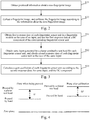
- Fig. 1 is a schematic diagram of each layer of a fingerprint module with a silkscreened logo pattern on a cover according to an embodiment of the present disclosure.
- the following steps are included.
- a pattern is silkscreened on the cover;
- a first ground colour is silkscreened based on the first step;
- a second ground colour is silkscreened based on the second step;
- a module obtained in the third step is attached to a chip via glue, to form the fingerprint module.
- the chip includes multiple fingerprint sensor units arranged in an array manner.
- a part of the silkscreened logo layer is embedded in a glue layer. Because dielectric constants of the silkscreened logo layer and the glue layer are different, capacitance values from a surface of the cover to the fingerprint sensor units in the chip are different. As an example, capacitance values of points A and B in Fig. 1 are different.
- data collected by the fingerprint sensor units may be considered as a combination of capacitance between a fingerprint by a finger press and the surface of the cover, as well as capacitance between the surface of the cover and the fingerprint sensor units in the chip. The capacitance between the surface of the cover and the fingerprint sensor units in the chip is fixed for a particular module.
- Fig. 2 is a schematic flowchart of a method for calibrating a fingerprint image according to an embodiment of the present disclosure.
- the method includes the following steps.
- the non-fingerprint image refers to the non-fingerprint image overlapped on a fingerprint image during fingerprint image collection.
- the non-fingerprint image may be specifically the above logo image.
- the logo image is used as an example. After the logo image is silkscreened on a cover, the information about the logo image does not change. Therefore, the information about the non-fingerprint image may be calculated and stored before delivery of an intelligent terminal.
- the information about the non-fingerprint image may be calculated and stored in a mass production test phase of a fingerprint module (module for short).
- the information about the non-fingerprint image may be calculated and stored in a production test phase of a device.
- a procedure of obtaining the information about the non-fingerprint image may include a step of:
- X is a detection signal of the fingerprint sensor unit (input to a surface of the module),
- Y is data output by the fingerprint sensor unit,
- B is a direct current (DC) component of a fingerprint sensor unit circuit, i.e., response data in the case of no press input, and
- Kr is the gain coefficient of each fingerprint sensor unit.
- Kr may serve as information about the logo image.
- a procedure of calculating the gain coefficient Kr includes the following steps.
- response data (to be differentiated from subsequent response data, referred to as the first response data herein) is the DC component of the corresponding fingerprint sensor unit.
- the conductive planar test head is a module that may generate same input for each fingerprint sensor unit in the fingerprint module.
- the conductive planar test head is a conductive planar rubber head.
- the conductive planar rubber head may be a rubber head with one face being a plane.
- the rubber head contains a conductive material with a resistance less than 800 ohms.
- the plane of the conductive planar rubber head may press onto the fingerprint module, and the planar rubber head is kept well grounded, so that the input X for the fingerprint sensor units are the same.
- response data of each fingerprint sensor unit may be detected.
- the response data is referred to as the second response data.
- Kr is the gain coefficient
- data1 is the second response data
- C is the same input
- B is the DC component
- the gain coefficient of each sensor unit may be calculated according to the above operation, and the gain coefficient serves as the information about the logo image for subsequent calibration of the fingerprint image.
- CaliData data 2 ⁇ B + Kr * B / Kr + C * avgKr ⁇ C ;
- CaliData is data about the fingerprint image after the calibration
- data2 is data about the fingerprint image before the calibration
- Kr is the gain coefficient
- B is the DC component
- C is the same input
- avgKr is an average value of the gain coefficients of all the fingerprint sensor units.
- Step 2 impact brought by C is eliminated.
- a fingerprint signal may be considered as a sum of a finger press on the plane and a finger's fingerprint signal.
- the finger's fingerprint signal generates different data on the fingerprint sensor units and is a valid signal.
- Data generated by the finger press on the plane is completely the same for each fingerprint sensor unit, and is similar to the input value C of the conductive planar rubber head.
- Both the finger press on the plane and the input value C of the conductive planar rubber head are equivalent input signals on each fingerprint sensor unit, affect only the overall data range rather than the valid fingerprint signal, and have a fixed difference ⁇ .
- Table 1 shows an expression of each plane shown in Fig. 4 .
- Kr in Kr*C in the above formula is replaced by an average value avgKr of gains Kr of all the fingerprint sensor units in the module.
- the prestored information about the non-fingerprint image is obtained, and the collected fingerprint image is calibrated according to the information about the non-fingerprint image. This can remove a non-fingerprint image part from a collected fingerprint image and improve accuracy of the collected fingerprint image, thereby improving a fingerprint recognition effect.
- Kr may be stored in different phases, and details are separately presented in the following embodiments.
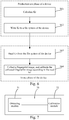
- Fig. 5 is a schematic flowchart of a method for calibrating a fingerprint image according to another embodiment of the present disclosure.
- Kr is obtained and stored in mass production test phase of fingerprint modules.
- the method in this embodiment includes the following steps.
- S52 a format of Kr is converted into a storage format for a non-volatile memory, and the Kr is written to the non-volatile memory of a fingerprint module.
- Kr may be a decimal.
- the non-volatile memory generally stores data of an integer format. Therefore, it is desired to convert the decimal into an integer for being stored in the non-volatile memory.
- mapping relationship between a decimal and an integer may be established, and the format of Kr may be converted into the storage format for the non-volatile memory according to the mapping relationship.
- S51 and S52 may be performed in the mass production test phase of fingerprint modules.
- the following procedure may be performed in an in-use phase of a device:
- the Kr of the storage format is restored to the original Kr by a reverse process of converting the original Kr into the Kr of the storage format.
- CaliData data 2 ⁇ B + Kr * B / Kr + C * avgKr ⁇ C ,
- CaliData is data about the fingerprint image after the calibration
- data2 is data about the fingerprint image before the calibration
- Kr is a gain coefficient
- B is a DC component
- C is a same input
- avgKr is an average value of gain coefficients of all fingerprint sensor units.
- the calibration of the fingerprint image may be achieved by the above calibration formula.
- the prestored information about the non-fingerprint image is obtained, and the collected fingerprint image is calibrated according to the information about the non-fingerprint image.
- This can remove a non-fingerprint image part from a collected fingerprint image and improve accuracy of the collected fingerprint image, thereby improving a fingerprint recognition effect. Further, it is applicable for calculation and storage of Kr in the mass production test phase of modules by converting Kr into Kr of the storage format for the non-volatile memory.
- Fig. 6 is a schematic flowchart of a method for calibrating a fingerprint image according to still another embodiment of the present disclosure.
- Kr is obtained and stored in the production test phase of a device.
- the method in this embodiment includes the following steps.
- the file system of the device may store data in a decimal format.
- S61 and S62 may be performed in the production test phase of the device.
- the following procedure may be performed in an in-use phase of the device:
- CaliData data 2 ⁇ B + Kr * B / Kr + C * avgKr ⁇ C ,
- CaliData is data about the fingerprint image after the calibration
- data2 is data about the fingerprint image before the calibration
- Kr is a gain coefficient
- B is a DC component
- C is a same input
- avgKr is an average value of gain coefficients of all fingerprint sensor units.
- the calibration of the fingerprint image may be achieved by the above calibration formula.
- the prestored information about the non-fingerprint image is obtained, and the collected fingerprint image is calibrated according to the information about the non-fingerprint image.
- This can remove a non-fingerprint image part from a collected fingerprint image and improve accuracy of the collected fingerprint image, thereby improving a fingerprint recognition effect. Further, it is applicable for calculation and storage of Kr in the production test phase of the device by storing Kr into the file system of the device.
- Fig. 7 is a schematic structural diagram of an apparatus for calibrating a fingerprint image according to an embodiment of the present disclosure.
- the apparatus 70 includes an obtaining module 71 and a calibration module 72.
- the obtaining module 71 is configured to obtain prestored information about a non-fingerprint image.
- the calibration module 72 is configured to collect a fingerprint image and calibrate the fingerprint image according to the information about the non-fingerprint image.
- the apparatus 70 further includes:
- the obtaining module 71 is specifically configured to:
- the apparatus 70 further includes:
- the obtaining module 71 is specifically configured to read the information about the non-fingerprint image from the file system.
- the calculation module 73 is specifically configured to:
- calculation module 73 is further specifically configured to:
- the calculation module 73 calculates the gain coefficient of each fingerprint sensor unit by a calculation formula:
- the conductive planar test head is a conductive planar rubber head.
- CaliData is data about the fingerprint image after the calibration
- data2 is data about the fingerprint image before the calibration
- Kr is a gain coefficient
- B is a DC component
- C is same input
- avgKr is an average value of the gain coefficients of all the fingerprint sensor units.
- the prestored information about the non-fingerprint image is obtained, and the collected fingerprint image is calibrated according to the information about the non-fingerprint image. This can remove a non-fingerprint image part from a collected fingerprint image and improve accuracy of the collected fingerprint image, thereby improving a fingerprint recognition effect.
- Fig. 10 is a schematic structural diagram of a terminal according to an embodiment of the present disclosure.
- the terminal 100 includes a housing 101, a processor 102, a memory 103, a circuit board 104 and a power supply circuit 105, wherein the circuit board 104 is disposed in space enclosed by the housing 101, the processor 102 and the memory 103 are disposed on the circuit board 104; the power supply circuit 105 is configured to supply power to each circuit or component of the terminal; the memory 103 is configured to store an executable program code; and the processor 102 is configured to execute a program corresponding to the executable program code by reading the executable program code stored in the memory, to perform the following steps of:
- non-volatile computer storage medium wherein the non-volatile computer storage medium stores one or more modules, to perform the following steps of:
- the prestored information about the non-fingerprint image is obtained, and the collected fingerprint image is calibrated according to the information about the non-fingerprint image. This can remove a non-fingerprint image part from a collected fingerprint image and improve accuracy of the collected fingerprint image, thereby improving a fingerprint recognition effect.
- parts of the present disclosure may be implemented by using hardware, software, firmware, or a combination thereof.
- multiple steps or methods may be implemented by using software or firmware that are stored in a memory and are executed by a proper instruction execution system.
- any one or a combination of the following technologies that are known in the art may be used for implementation: a discrete logic circuit having a logic gate circuit configured to implement a logic function on a data signal, an application-specific integrated circuit having a proper combined logic gate circuit, a programmable gate array (PGA), a field programmable gate array (FPGA), and the like.
- functional units in the embodiments of the present disclosure may be integrated into one processing module, or each of the units may exist alone physically, or two or more units are integrated into one module.
- the above integrated module may be implemented in a form of hardware, or may be implemented in a form of a software functional module.
- the integrated module When the integrated module is implemented in a form of a software functional module and sold or used as an independent product, the integrated module may be stored in a computer readable storage medium.
- the storage medium mentioned above may be a read-only memory, a magnetic disk, an optical disc, or the like.
Landscapes
- Engineering & Computer Science (AREA)
- Theoretical Computer Science (AREA)
- Physics & Mathematics (AREA)
- General Physics & Mathematics (AREA)
- Multimedia (AREA)
- Human Computer Interaction (AREA)
- Computer Vision & Pattern Recognition (AREA)
- Data Mining & Analysis (AREA)
- Library & Information Science (AREA)
- Databases & Information Systems (AREA)
- General Engineering & Computer Science (AREA)
- Quality & Reliability (AREA)
- Image Input (AREA)
Applications Claiming Priority (1)
| Application Number | Priority Date | Filing Date | Title |
|---|---|---|---|
| PCT/CN2016/076998 WO2017161501A1 (fr) | 2016-03-22 | 2016-03-22 | Procédé et dispositif permettant de corriger une image d'empreinte digitale, et terminal |
Publications (2)
| Publication Number | Publication Date |
|---|---|
| EP3276531A1 true EP3276531A1 (fr) | 2018-01-31 |
| EP3276531A4 EP3276531A4 (fr) | 2018-04-18 |
Family
ID=57341017
Family Applications (1)
| Application Number | Title | Priority Date | Filing Date |
|---|---|---|---|
| EP16894856.0A Withdrawn EP3276531A4 (fr) | 2016-03-22 | 2016-03-22 | Procédé et dispositif permettant de corriger une image d'empreinte digitale, et terminal |
Country Status (5)
| Country | Link |
|---|---|
| US (1) | US10706254B2 (fr) |
| EP (1) | EP3276531A4 (fr) |
| KR (1) | KR101915426B1 (fr) |
| CN (1) | CN106164933B (fr) |
| WO (1) | WO2017161501A1 (fr) |
Cited By (2)
| Publication number | Priority date | Publication date | Assignee | Title |
|---|---|---|---|---|
| EP3649578A4 (fr) * | 2017-07-07 | 2021-04-07 | Fingerprint Cards AB | Procédé de système de détection d'empreintes digitales permettant l'authentification d'un utilisateur en fonction de données d'empreintes digitales |
| US11301664B2 (en) | 2018-09-12 | 2022-04-12 | Fingerprint Cards Anacatum Ip Ab | Reconstruction of fingerprint subimages |
Families Citing this family (17)
| Publication number | Priority date | Publication date | Assignee | Title |
|---|---|---|---|---|
| US10713466B2 (en) * | 2014-03-07 | 2020-07-14 | Egis Technology Inc. | Fingerprint recognition method and electronic device using the same |
| CN106164933B (zh) * | 2016-03-22 | 2019-06-07 | 深圳市汇顶科技股份有限公司 | 指纹图像的校正方法、装置和终端 |
| WO2018141119A1 (fr) * | 2017-02-03 | 2018-08-09 | 华为技术有限公司 | Procédé, appareil et terminal d'acquisition d'empreintes digitales |
| GB201704847D0 (en) * | 2017-03-27 | 2017-05-10 | Zwipe As | Callibration method |
| US11232274B2 (en) | 2017-03-10 | 2022-01-25 | Fingerprint Cards Anacatum Ip Ab | Suppressing impairment data in fingerprint images |
| CN107657240B (zh) * | 2017-10-09 | 2020-11-24 | 上海天马微电子有限公司 | 一种显示装置及其指纹识别校准方法、以及电子设备 |
| CN107742111B (zh) * | 2017-11-03 | 2021-11-02 | 北京小米移动软件有限公司 | 身份识别方法及装置、存储介质 |
| CN108182424B (zh) * | 2018-01-29 | 2020-05-22 | 上海天马微电子有限公司 | 显示装置及其指纹识别方法 |
| CN109711308B (zh) * | 2018-12-19 | 2021-06-01 | 北京集创北方科技股份有限公司 | 指纹组件、电子设备及其指纹信号处理方法 |
| WO2020210954A1 (fr) * | 2019-04-15 | 2020-10-22 | 深圳市汇顶科技股份有限公司 | Procédé et appareil d'étalonnage d'image et dispositif électronique |
| CN110097031B (zh) * | 2019-05-14 | 2023-07-25 | 上海菲戈恩微电子科技有限公司 | 一种屏下光学指纹图像的校正方法和装置 |
| CN110187806B (zh) * | 2019-05-22 | 2023-04-18 | Oppo广东移动通信有限公司 | 指纹模板录入方法及相关装置 |
| WO2020232696A1 (fr) * | 2019-05-23 | 2020-11-26 | 深圳市汇顶科技股份有限公司 | Procédé et dispositif d'étalonnage pour identification d'empreintes digitales optique et équipement électronique |
| CN112417951B (zh) * | 2020-09-30 | 2022-06-24 | 北京极豪科技有限公司 | 指纹图像校准方法、装置、电子设备及存储介质 |
| CN114359984B (zh) * | 2020-09-30 | 2026-02-03 | 比亚迪半导体股份有限公司 | 指纹模组偏差消除系统、方法和指纹模组图像调整方法 |
| CN113723167B (zh) * | 2021-04-02 | 2024-07-02 | 荣耀终端有限公司 | 一种指纹识别方法及电子设备 |
| US11657643B1 (en) * | 2022-01-17 | 2023-05-23 | Novatek Microelectronics Corp. | Fingerprint sensing device |
Family Cites Families (26)
| Publication number | Priority date | Publication date | Assignee | Title |
|---|---|---|---|---|
| JPH07122903B2 (ja) * | 1987-05-30 | 1995-12-25 | 川崎製鉄株式会社 | 画像の背景消去方法 |
| JP3590671B2 (ja) | 1995-05-23 | 2004-11-17 | ティーエム・ティーアンドディー株式会社 | 負荷時タップ切換装置 |
| US6125192A (en) * | 1997-04-21 | 2000-09-26 | Digital Persona, Inc. | Fingerprint recognition system |
| US5995642A (en) * | 1997-06-30 | 1999-11-30 | Aetex Biometric Corporation | Method for automatic fingerprint classification |
| US6068184A (en) * | 1998-04-27 | 2000-05-30 | Barnett; Donald A. | Security card and system for use thereof |
| US7126631B1 (en) * | 1999-06-30 | 2006-10-24 | Intel Corporation | Sensing with defective cell detection |
| US6658164B1 (en) * | 1999-08-09 | 2003-12-02 | Cross Match Technologies, Inc. | Calibration and correction in a fingerprint scanner |
| FR2826151B1 (fr) * | 2001-06-13 | 2004-12-17 | Sagem | Procede de reconnaissance d'empreintes digitales par coloration et systeme informatique pour mettre en oeuvre ledit procede |
| JP2003075135A (ja) * | 2001-08-31 | 2003-03-12 | Nec Corp | 指紋画像入力装置および指紋画像による生体識別方法 |
| JP4546168B2 (ja) * | 2004-06-28 | 2010-09-15 | 富士通株式会社 | 生体認証システムの登録方法、生体認証システム及びそのプログラム |
| CN101605399A (zh) * | 2008-06-13 | 2009-12-16 | 英华达(上海)电子有限公司 | 一种实现手语识别的移动终端及方法 |
| US8577091B2 (en) * | 2009-07-17 | 2013-11-05 | The University Of Maryland | Method and apparatus for authenticating biometric scanners |
| CN101853383B (zh) * | 2010-05-17 | 2012-09-05 | 清华大学 | 高分辨率掌纹方向场提取方法 |
| US8547111B2 (en) * | 2010-07-06 | 2013-10-01 | Sharp Kabushiki Kaisha | Array element circuit and active matrix device |
| CN102208021B (zh) * | 2011-07-21 | 2012-12-19 | 中国人民解放军国防科学技术大学 | 一种指纹图像分割方法 |
| US8824792B2 (en) * | 2012-07-25 | 2014-09-02 | Ib Korea Ltd. | Image element brightness adjustment |
| US9576176B2 (en) * | 2013-07-22 | 2017-02-21 | Apple Inc. | Noise compensation in a biometric sensing device |
| US9552525B2 (en) * | 2013-09-08 | 2017-01-24 | Apple Inc. | Noise reduction in biometric images |
| CN105868679B (zh) * | 2015-01-23 | 2017-11-28 | 深圳市汇顶科技股份有限公司 | 指纹信息的动态更新方法和指纹识别装置 |
| CN204442446U (zh) * | 2015-03-13 | 2015-07-01 | 深圳欧菲光科技股份有限公司 | 用于移动终端的背盖结构及其移动终端 |
| CN105205470A (zh) * | 2015-09-29 | 2015-12-30 | 上海箩箕技术有限公司 | 指纹成像模组 |
| CN105243370A (zh) * | 2015-10-19 | 2016-01-13 | 广东欧珀移动通信有限公司 | 一种指纹识别方法、指纹识别装置和移动终端 |
| CN106164933B (zh) * | 2016-03-22 | 2019-06-07 | 深圳市汇顶科技股份有限公司 | 指纹图像的校正方法、装置和终端 |
| CN110431564B (zh) * | 2017-10-13 | 2020-11-17 | 指纹卡有限公司 | 用于指纹图像增强的方法和系统 |
| JP7122903B2 (ja) * | 2018-07-27 | 2022-08-22 | マクセル株式会社 | 路面映像投射装置及び車両用灯具 |
| CN109711308B (zh) * | 2018-12-19 | 2021-06-01 | 北京集创北方科技股份有限公司 | 指纹组件、电子设备及其指纹信号处理方法 |
-
2016
- 2016-03-22 CN CN201680000664.5A patent/CN106164933B/zh active Active
- 2016-03-22 KR KR1020177030869A patent/KR101915426B1/ko active Active
- 2016-03-22 EP EP16894856.0A patent/EP3276531A4/fr not_active Withdrawn
- 2016-03-22 WO PCT/CN2016/076998 patent/WO2017161501A1/fr not_active Ceased
-
2017
- 2017-10-23 US US15/790,782 patent/US10706254B2/en active Active
Cited By (2)
| Publication number | Priority date | Publication date | Assignee | Title |
|---|---|---|---|---|
| EP3649578A4 (fr) * | 2017-07-07 | 2021-04-07 | Fingerprint Cards AB | Procédé de système de détection d'empreintes digitales permettant l'authentification d'un utilisateur en fonction de données d'empreintes digitales |
| US11301664B2 (en) | 2018-09-12 | 2022-04-12 | Fingerprint Cards Anacatum Ip Ab | Reconstruction of fingerprint subimages |
Also Published As
| Publication number | Publication date |
|---|---|
| WO2017161501A1 (fr) | 2017-09-28 |
| CN106164933B (zh) | 2019-06-07 |
| KR101915426B1 (ko) | 2018-11-05 |
| US10706254B2 (en) | 2020-07-07 |
| US20180060643A1 (en) | 2018-03-01 |
| CN106164933A (zh) | 2016-11-23 |
| EP3276531A4 (fr) | 2018-04-18 |
| KR20170131621A (ko) | 2017-11-29 |
Similar Documents
| Publication | Publication Date | Title |
|---|---|---|
| EP3276531A1 (fr) | Procédé et dispositif permettant de corriger une image d'empreinte digitale, et terminal | |
| US10345980B2 (en) | Capacitive detection device, method and pressure detection system | |
| US9600128B2 (en) | Touch sensitive device and touch determination method thereof | |
| US20110157083A1 (en) | Resistive touch apparatus | |
| CN103329074A (zh) | 用于使用所估计偏转响应来确定物体信息的系统和方法 | |
| CN112445357B (zh) | 校准方法、装置及存储介质 | |
| JP7137488B2 (ja) | センサ装置 | |
| US9489083B2 (en) | Touch panel controller, touch sensor system, and electronic device | |
| CN104981761A (zh) | 触控面板设备和方法 | |
| KR20180104721A (ko) | 유도 전극의 초기 거리의 변화를 확정하는 방법 | |
| US20160313205A1 (en) | Drift Compensation for Force Sensing Devices | |
| Sánchez-Durán et al. | Hysteresis correction of tactile sensor response with a generalized Prandtl–Ishlinskii model | |
| US9983752B2 (en) | Pressure detection method for in-cell touch display and mobile device using the same | |
| US9377883B2 (en) | Touch sensing method, recording medium in which program for realizing the same is recorded, and touch sensing system | |
| US20150193068A1 (en) | Method and apparatus for sensing touch pressure of touch panel and touch sensing apparatus using the same | |
| CN109634455B (zh) | 一种基于触摸屏的校准方法及校准系统 | |
| CN107184209A (zh) | 检测皮肤水分的方法和终端设备 | |
| TWI660299B (zh) | 輸入裝置與其控制方法及程式 | |
| US20150309659A1 (en) | Method and touch apparatus for calibrating coordinate value near edge of touch panel | |
| CN118819341A (zh) | 信号处理方法、触控芯片及触控装置 | |
| CN105094434A (zh) | 一种手势识别环境校准方法、系统及电子设备 | |
| JP2004062729A (ja) | 筆文字入力装置 | |
| CN108304760B (zh) | 检测手指上手和离手之方法和电子装置 | |
| CN111352530A (zh) | 电容按键信号阈值范围的调整方法、装置及终端设备 | |
| CN106575134A (zh) | 用于在触摸敏感表面上定位交互的方法和设备 |
Legal Events
| Date | Code | Title | Description |
|---|---|---|---|
| PUAI | Public reference made under article 153(3) epc to a published international application that has entered the european phase |
Free format text: ORIGINAL CODE: 0009012 |
|
| 17P | Request for examination filed |
Effective date: 20171024 |
|
| AK | Designated contracting states |
Kind code of ref document: A1 Designated state(s): AL AT BE BG CH CY CZ DE DK EE ES FI FR GB GR HR HU IE IS IT LI LT LU LV MC MK MT NL NO PL PT RO RS SE SI SK SM TR |
|
| AX | Request for extension of the european patent |
Extension state: BA ME |
|
| A4 | Supplementary search report drawn up and despatched |
Effective date: 20180316 |
|
| RIC1 | Information provided on ipc code assigned before grant |
Ipc: G06T 7/80 20170101ALI20180309BHEP Ipc: G06F 17/30 20060101ALI20180309BHEP Ipc: G06K 9/03 20060101ALI20180309BHEP Ipc: G06K 9/00 20060101AFI20180309BHEP |
|
| 17Q | First examination report despatched |
Effective date: 20190130 |
|
| DAV | Request for validation of the european patent (deleted) | ||
| DAX | Request for extension of the european patent (deleted) | ||
| STAA | Information on the status of an ep patent application or granted ep patent |
Free format text: STATUS: THE APPLICATION HAS BEEN WITHDRAWN |
|
| 18W | Application withdrawn |
Effective date: 20200401 |