EP3276533A2 - Wärmemustersensor mit gemeinsam genutzten heizelementen - Google Patents
Wärmemustersensor mit gemeinsam genutzten heizelementen Download PDFInfo
- Publication number
- EP3276533A2 EP3276533A2 EP17183876.6A EP17183876A EP3276533A2 EP 3276533 A2 EP3276533 A2 EP 3276533A2 EP 17183876 A EP17183876 A EP 17183876A EP 3276533 A2 EP3276533 A2 EP 3276533A2
- Authority
- EP
- European Patent Office
- Prior art keywords
- pixels
- pixel
- electrically conductive
- reading
- line
- Prior art date
- Legal status (The legal status is an assumption and is not a legal conclusion. Google has not performed a legal analysis and makes no representation as to the accuracy of the status listed.)
- Withdrawn
Links
Images


Classifications
-
- G—PHYSICS
- G06—COMPUTING OR CALCULATING; COUNTING
- G06V—IMAGE OR VIDEO RECOGNITION OR UNDERSTANDING
- G06V40/00—Recognition of biometric, human-related or animal-related patterns in image or video data
- G06V40/10—Human or animal bodies, e.g. vehicle occupants or pedestrians; Body parts, e.g. hands
- G06V40/12—Fingerprints or palmprints
- G06V40/13—Sensors therefor
- G06V40/1306—Sensors therefor non-optical, e.g. ultrasonic or capacitive sensing
-
- G—PHYSICS
- G01—MEASURING; TESTING
- G01J—MEASUREMENT OF INTENSITY, VELOCITY, SPECTRAL CONTENT, POLARISATION, PHASE OR PULSE CHARACTERISTICS OF INFRARED, VISIBLE OR ULTRAVIOLET LIGHT; COLORIMETRY; RADIATION PYROMETRY
- G01J5/00—Radiation pyrometry, e.g. infrared or optical thermometry
- G01J5/10—Radiation pyrometry, e.g. infrared or optical thermometry using electric radiation detectors
- G01J5/34—Radiation pyrometry, e.g. infrared or optical thermometry using electric radiation detectors using capacitors, e.g. pyroelectric capacitors
-
- G—PHYSICS
- G01—MEASURING; TESTING
- G01R—MEASURING ELECTRIC VARIABLES; MEASURING MAGNETIC VARIABLES
- G01R19/00—Arrangements for measuring currents or voltages or for indicating presence or sign thereof
- G01R19/10—Measuring sum, difference or ratio
-
- G—PHYSICS
- G01—MEASURING; TESTING
- G01R—MEASURING ELECTRIC VARIABLES; MEASURING MAGNETIC VARIABLES
- G01R19/00—Arrangements for measuring currents or voltages or for indicating presence or sign thereof
- G01R19/32—Compensating for temperature change
-
- G—PHYSICS
- G06—COMPUTING OR CALCULATING; COUNTING
- G06V—IMAGE OR VIDEO RECOGNITION OR UNDERSTANDING
- G06V40/00—Recognition of biometric, human-related or animal-related patterns in image or video data
- G06V40/10—Human or animal bodies, e.g. vehicle occupants or pedestrians; Body parts, e.g. hands
- G06V40/12—Fingerprints or palmprints
- G06V40/13—Sensors therefor
- G06V40/1329—Protecting the fingerprint sensor against damage caused by the finger
-
- H—ELECTRICITY
- H03—ELECTRONIC CIRCUITRY
- H03K—PULSE TECHNIQUE
- H03K17/00—Electronic switching or gating, i.e. not by contact-making and –breaking
- H03K17/94—Electronic switching or gating, i.e. not by contact-making and –breaking characterised by the way in which the control signals are generated
- H03K17/941—Electronic switching or gating, i.e. not by contact-making and –breaking characterised by the way in which the control signals are generated using an optical detector
-
- H—ELECTRICITY
- H03—ELECTRONIC CIRCUITRY
- H03K—PULSE TECHNIQUE
- H03K17/00—Electronic switching or gating, i.e. not by contact-making and –breaking
- H03K17/94—Electronic switching or gating, i.e. not by contact-making and –breaking characterised by the way in which the control signals are generated
- H03K17/96—Touch switches
- H03K17/962—Capacitive touch switches
Definitions
- the invention relates to a thermal pattern sensor in which the heating elements are pooled so that each of the heating elements is able to heat several rows of pixels.
- This thermal pattern sensor advantageously corresponds to a fingerprint sensor by thermal detection.
- a fingerprint sensor comprises thermal detection means.
- These thermal detection means may correspond to pyroelectric elements, diodes, thermistors or any other temperature-sensitive element that makes it possible to convert a temperature variation into a variation of potential or of electric current.
- the detection of a fingerprint can be performed by so-called "passive" sensors exploiting a temperature difference between the finger and the sensor, as described in the documents US 4,394,773 , US 4,429,413 and US 6,289,114 .
- These sensors have the disadvantage of making a measurement that depends solely on the temperature difference between the finger and the sensor. It may therefore happen that the level of the signal obtained is zero when the finger and the sensor are at the same temperature (for example when the finger remains a certain time on the sensor), or that the contrast of the captured images varies and then raises problems when processing images later.
- each pixel comprises a pyroelectric capacitor formed of two conductive electrodes between which a portion of pyroelectric material is disposed, and a heating element.
- This heating element dissipates a certain amount of heat in the pixel, and the heating of the pixel is measured after a certain acquisition time, called integration time, in the presence of the finger on the sensor.
- such a sensor can measure the heat capacity, also called specific heat or specific heat capacity, of an element in contact with the sensor.
- the measurements obtained also depend on the thermal conductivity between the sensor and the part of the element (peak or valley in the case of a fingerprint) in the presence.
- the pixels of this sensor are coupled to heating elements generally using the Joule effect which dissipate heat from a resistive element which is traversed by a current.
- One of the levels of the technological stack forming the pixels is advantageously used to form these heating elements.
- the sensor comprises transistors of the TFT ("Thin-Film Transistor" or thin-film transistor) type produced on a glass or plastic substrate.
- the pixels of such a sensor are arranged by forming a matrix of several rows and several columns.
- the reading of the pixels is generally done line by line.
- the heating elements can then also be controlled by line using a transistor at the head of each line, thus avoiding the addition of control transistors in each of the pixels.
- Each line of heating elements is for example connected, on one side of the matrix of pixels, to the ground, and on the other side to control transistor associated with the pixel line and connected to a power supply adapted to control the current flowing through the heating elements, and therefore the thermal power injected by the Joule effect into the pixels by these heating elements.
- the line of heating elements associated with the line of pixels to be read is activated by making circulating a heating current in this line of heating elements.
- Each of the pixels comprises at least one selection transistor, and the pixel selection transistors of each column of pixels are connected to a conductive line which is itself connected to a read circuit.
- the selection transistors of the pixels of this line are set to the on state, which makes it possible to connect the active nodes of the pixels of this line to the reading circuits at the foot of the line. each of the columns of pixels.
- Blocked selection transistors of the pixels belonging to the other pixel lines prevent the displacement of charges from these other pixels to the readout circuits.
- Other transistors may also be present in each pixel, especially when the pixels are read in voltage and they require the presence of a reset transistor and a voltage follower transistor, or the sensor also forms a sensor wherein a transistor is present in each pixel for connecting a photodiode of each pixel to a dedicated read circuit.
- the transistors are made by lithography techniques allowing their realization with a good resolution.
- the pyroelectric material is then deposited and the upper electrodes of the pyroelectric capacitors are produced.
- the heating elements must then be made.
- An object of the present invention is to provide a thermal pattern sensor comprising heating elements compatible with a realization by printing while allowing to obtain a good resolution of the pixels.
- the invention proposes a thermal pattern sensor comprising a matrix of several lines and columns of pixels, each pixel comprising at least one pyroelectric capacitance formed by at least one portion of pyroelectric material disposed between a lower electrode and a top electrode, wherein a first one of the lower and upper electrodes forms a reading electrode of the pixel, and further comprising a plurality of electrically conductive portions each capable of Joule heating independently of the other electrically conductive portions, the pyroelectric material portions of the pyroelectric capacitors. pixels of at least two adjacent pixel lines associated with the electrically conductive portion, and arranged facing at least a portion of the surface of the reading electrodes of each of the pixels of the lines associated with the electrically conductive portion.
- each of the electrically conductive portions therefore forms the heating element of at least two adjacent pixel lines.
- the resolution necessary for producing these electrically conductive portions is divided by a factor at least equal to two with respect to the resolution of the pixels.
- the electrically conductive portions forming the heating elements can therefore be made with techniques that do not make it possible to obtain a resolution equal to that of the pixels of the sensor, for example by printing.
- the element comprising the thermal pattern intended to be detected by the sensor is intended to be in physical contact with the sensor, that is to say placed against the sensor during the detection of this thermal pattern.
- Each of the electrically conductive portions may be disposed facing the entire surface of the reading electrode of each of the pixels of the lines associated with the electrically conductive portion.
- each of the electrically conductive portions may be arranged opposite a portion of the surface of the reading electrode of each of the pixels of the lines associated with the electrically conductive portion, the surfaces of the reading electrodes of the pixels being in viewed electrically conductive portions may be substantially equal to each other.
- the electrically conductive portions forming the heating elements do not completely cover the reading electrodes of the pixels, a similar heating between all the pixels heated by such an electrically conductive portion is obtained thanks to the identical overlap of the reading electrodes of these pixels. by the electrically conductive portion.
- the step of reading the amount of electrical charges received by the read circuits may be followed by a step of stopping the application of the heating voltage to the ends of the electrically conductive portion associated with said pixel line.
- control circuit may be able to control the successive reading of several rows of pixels such that two rows of pixels read in succession are associated with different electrically conductive portions.
- control circuit may be able to control the successive reading of several rows of pixels such that two rows of pixels read in succession are associated with different electrically conductive portions.
- the reading electrodes of pixels of the same column and belonging to two adjacent pixel lines associated with different electrically conductive portions may be electrically connected to each other. This configuration makes it possible to reduce the number of selection transistors and the number of selection lines necessary to perform the reading of the pixels of the sensor.
- the senor according to this second embodiment comprises a larger number of read columns and a larger number of read circuits. Since the rows of pixels heated by the same electrically conductive portion can be read simultaneously, the reading of the pixels is simplified, and it becomes unnecessary to respect a waiting time between two successive readings of two lines of pixels associated with the same electrically conductive portion providing heating of these two lines of pixels.
- the step of reading the quantity of electrical charges received by the reading circuits may be followed by a step of stopping the application of the heating voltage to the ends of the electrically conductive portion associated with said lines of pixels.
- the control circuit may be able to apply at least a second non-zero heating voltage to the ends of at least one electrically conductive portion adjacent to the electrically conductive portion associated with the line of pixels read.
- the heat generated by the electrically conductive portion adjacent to the electrically conductive portion associated with the read pixel line contributes to the heating of the pixel line read.
- the diathermy phenomenon is here used judiciously to inject more heat into the read pixel line and thus obtain reading signals delivered by the read pixels which are more important.
- the heating produced by the one or more other electrically conductive portions located next to the read pixel line may be implemented such that a heating power dissipated by this or these other electrically conductive portions is smaller than that dissipated by the electrically conductive portion associated with the pixel line read.
- the heat is mainly provided by the electrically conductive portion associated with the read pixel line and not by the lateral heating produced by the other electrically conductive portion or portions. This control of the heat provided to the read pixel line limits the undesirable effects of diathermy.
- the sensor may further comprise a substrate on which the pyroelectric capacitances of the pixels are arranged, the lower electrode of the pyroelectric capacitance of each pixel forming the reading electrode of the pixel and being disposed between the substrate and the portion of pyroelectric material of the pyroelectric capacitance of the pixel.
- the electrically conductive portions can form the upper electrodes of the pyroelectric capacitances of the pixels, that is to say the electrodes the closest to the surface of the sensor on which is the element whose thermal pattern is measured.
- the thermal pattern sensor may further comprise a dielectric layer covering the upper electrode of each pixel of the matrix and a first electrically conductive layer disposed on said dielectric layer and forming an electromagnetic shielding of the sensor.
- the upper electrodes of the pyroelectric capacitances of the pixels may be formed by a second electrically conductive layer common to all the pixels of the matrix, capable of being electrically connected to an electrical reference potential and disposed between the electrically conductive portions and the electrodes. reading.
- This variant is advantageous because it makes it possible to have an arrangement of the electrically conductive portions forming the heating elements as close as possible to the element present on the sensor and whose thermal pattern is intended to be detected.
- the reading electrodes of the pixels may be formed by elements of electrically conductive material which are distinct and electrically isolated from one another.
- the thermal pattern sensor may be an active thermal fingerprint sensor made on a flexible substrate with IGZO-based TFT type transistors.
- the lower electrodes can be made above the transistors, during the lithography steps forming the sensor transistors, which allows these lower electrodes to be made with a high resolution.
- the pyroelectric material is deposited on the lower electrodes, and the upper electrodes, advantageously formed by the electrically conductive portions corresponding to the pixel heating elements, are advantageously produced on the pyroelectric material by the implementation of low cost printing techniques.
- the invention also relates to a method for producing a thermal pattern sensor as described above, in which the electrically conductive portions are produced by printing.
- FIG. 1 shows a sectional view of a pyroelectric capacitance of a pixel 102, which forms the thermosensitive measuring element of the pixel 102, of a thermal pattern sensor 100.
- the sensor 100 comprises a substrate 104 corresponding for example to a glass substrate or a semiconductor substrate (for example silicon).
- a glass substrate 104 may be used when the sensor 100 is made with TFT transistors, while a semiconductor substrate 104, for example silicon, may be used when the sensor 100 comprises transistors made in MOS technology.
- the substrate 104 may also be a flexible substrate, for example based on polyimide or PEN (polyethylene naphthalate) or PET (polyethylene terephthalate), on which the electronic elements of the sensor 100, such as TFT transistors, are made by printed electronic technology (for example via an embodiment with ink jet type writing heads) or by lithography.
- the transistors made on the substrate 104 and on which the pixels 102 are made are not represented on the figure 1 .
- the pixels 102 of the sensor 100 are made on the substrate 104 by forming a matrix of several lines and several columns of pixels 102.
- the pitch of the pixels 102 (corresponding to the spacing between the centers of two adjacent pixels), in the plane ( X, Y) (that is to say the plane of the substrate 104), is for example between about 25 microns and 100 microns. In the case of a sensor 100 with a resolution of 500 dpi, the pitch of the pixels 102 is equal to 50.8 ⁇ m.
- Each of the pixels 102 of the sensor 100 comprises measuring means, or detection, thermosensitive formed by a pyroelectric capacitance.
- Each pyroelectric capacitor comprises a portion 106 of pyroelectric material disposed between a lower electrode 108 and an upper electrode 110.
- the pyroelectric material of the portion 106 is advantageously P (VDF-TrFE) or PVDF.
- the pyroelectric material of the portion 106 may be AIN or PZT, or any other pyroelectric material adapted to form a pyroelectric capacitance.
- the thickness of the portion 106 is for example between about 500 nm and 10 microns.
- the electrodes 108, 110 each comprise at least one electrically conductive material, for example a metallic material such as titanium having a thickness of approximately 0.2 ⁇ m, and / or molybdenum and / or aluminum and / or conductive oxide such as ITO (indium and tin oxide) and / or a conductive polymer of thickness for example equal to several microns, for example about 4 microns.
- One of the electrodes 108, 110, advantageously the upper electrode 110, or each of the two electrodes 108, 110 may be formed by a stack of several electrically conductive materials, for example a Ti / TiN / AlCu stack.
- the thickness of each of the electrodes 108, 110 is for example between about 0.1 ⁇ m and 1 ⁇ m.
- the thickness of each of the electrodes 108, 110 may be greater, for example up to about 5 ⁇ m, especially when these electrodes are made by printing using materials such as silver, copper, carbon or PEDOT (poly (3,4-ethylenedioxythioph
- a protective layer 109 covers the upper electrode 110.
- the thickness of the protective layer 109 may be between a few microns and about 100 microns, or much larger (for example of the order of 300 microns or more).
- An upper face 113 of the protective layer 109 corresponds to the surface on which is located the thermal pattern to be detected, for example a finger whose fingerprint is intended to be detected.
- this material is subjected, once for the entire lifetime of the pyroelectric capacitor, to an electric field of approximately 100 volts per micron of thickness. of PVDF.
- the molecules inside the PVDF orient, and remain oriented, even when the PVDF is no longer subject to this electric field.
- the PVDF can thus be polarized by applying an initial bias voltage across the electrodes 108, 110.
- the parameter S corresponds to the surface of the portion 106 facing each of the electrodes 108, 110.
- the parameter ⁇ corresponds to the pyroelectric coefficient of the pyroelectric material of the portion 106.
- the pyroelectric coefficient ⁇ of the PVFD-TrFE is equal to about 32 ⁇ C / m 2 / K.
- parasitic capacitances Cp present, for example those linked to the gate of the read transistor in the case of a voltage reading circuit.
- the sign of the electrical voltage ⁇ V obtained between the electrodes 108, 110, or the direction of the current in the case of a current reading depends on the direction of the electric field with which the PVDF of the portion 106 was initially polarized. In the case of certain other pyroelectric materials such as aluminum nitride, this direction of initial polarization depends on the manner in which the pyroelectric material has been deposited, its order and its crystallographic orientation. In addition, the electrical voltage ⁇ V obtained, or the direction of the current, can be positive or negative depending on whether the temperature variation experienced by the pyroelectric capacitor is positive or negative.
- the sensor 100 also comprises heating elements dissipating a certain amount of heat in the pixels 102, and more particularly in the portion 106 of pyroelectric material, during the reading of the pixels 102.
- these heating elements are formed directly by one of the electrodes 108, 110 of each of the pyroelectric capacitors.
- the heating element of the pyroelectric capacitance of the pixel 102 is formed by the upper electrode 110.
- the other electrode of the pyroelectric capacitance, here the lower electrode 108 serves as reading electrode of the pixel 102.
- the heating of the portion 106 of pyroelectric material is obtained by circulating a current in the electrode for forming the heating element. But this The electrode is also used for the polarization of the pyroelectric capacitance.
- the heating resistor of each of the pixels 102 also serves to polarize an electrode of the pyroelectric capacitance formed by the portion 106 and the electrodes 108, 110 of each of the pixels 102 when measured by these pixels 102 (the polarization applied during a measurement is different from the initial polarization of the PVDF previously described).
- the use of one of the electrodes 108, 110 of the pixels 102 to form the heating elements is possible because the value of the electric potential applied to this electrode during a reading of the thermal pattern is constant.
- the figure 2 represents a top view of several pixels 102 of the sensor 100 according to a first embodiment.
- the lower electrodes 108 which correspond to the reading electrodes of the pixels on which the charges generated by the pyroelectric capacitors will be recovered for reading, are formed by elements of electrically conductive material which are distinct and electrically isolated from each other for each pixel 102. These conductive elements each have a rectangular section in the plane of the substrate 104 (plane (X, Y)), and are arranged next to each other in the form of a matrix to form the pixel array 102.
- the pyroelectric material is made in the form of a single portion 106, or a single layer 106, covering all the lower electrodes 108.
- the upper electrodes 110 of the pixels are formed by several electrically conductive portions 111, referenced 111.1 to 111.3 on the figure 2 , each forming the upper electrodes 110 of the pixels 102 belonging to at least two lines of adjacent pixels (two lines of adjacent pixels in the example of the figure 2 ).
- Each of the portions 111 has a first end 116 on which is applied a heating potential, and a second end 118 connected to another conductive portion 120 common to all the portions 111 and connected to ground.
- the electrical potentials applied to the first ends 116 of the portions 111 are similar from one portion 111 to the other.
- Each of the portions 111 is associated with at least two rows of pixels capable of being heated by the portion 111 associated therewith.
- the portion 111.1 is associated with the pixel lines 102.1 and 102.2
- the portion 111.2 is associated with the pixel lines 102.3 and 102.4
- the portion 111.3 is associated with the pixel lines 102.5 and 102.6.
- each of the portions 111.i forms a heating element capable of heating the rows of pixels 102. (2i) and 102. (2i-1), with i integer between 1 and n / 2 (for a sensor 100 comprising n rows of pixels).
- Each of the portions 111.i also forms the upper electrodes 110 of these pixel lines 102. (2i) and 102. (2i-1).
- a control circuit capable of controlling the switching on and off of the heating elements of the sensor 100, that is to say to control the circulation of a heating current in the portions 111, comprises, for example, an electrical connection applying an existing voltage in the sensor 100 on the end 116 of each of the portions 111. For example, if the end 118 of a portion 111 is connected to ground and a heating potential V heats is applied to the end 116 of this portion 111, a current then flows from the end 116 to the end 118 of the portion 111, causing Joule heating in the portion 111, and thus heating the pyroelectric material portions of the pixels 102 of the line of pixels heated by this portion 111.
- the value of the heating voltage is chosen as a function of the desired heating power, this power being a function in particular of the thickness of the portion 106 intended to be cha and the thickness of the protective layer 109, the pyroelectric coefficient of the material of the portion 106, the sensitivity of the read circuit, the noise level of the read circuit, and the integration time.
- the heating power is for example between about 0.1 mW and 10 mW.
- the electrically conductive portions 111 which serve as heating resistors for the pixels 102 also form the upper electrodes 110 of the pixels 102 which are disposed above the pyroelectric material and not the lower electrodes 108 because this arrangement makes it possible to connect to the ground of the sensor 100 the conductive portions of the pyroelectric capacitors that are closest to the outside of the sensor 100.
- Such an arrangement forms a protection vis-à-vis the electrostatic discharge (ESD) because if such a discharge occurs, there is then a path preferential for discharging the electric charges due to this discharge, which limits the voltage breakdown with fragile active elements of the sensor 100 such as transistors.
- ESD electrostatic discharge
- the heating elements are arranged under the portion of pyroelectric material 106 and form the lower electrodes 108.
- the portions 111 form conductive strips of uniform width, substantially equal to one another and each extending along two lines of pixels 102. The heat is thus uniformly diffused along each portion 111 which diffuses heat in the two rows of pixels 102 associated with this portion 111.
- each portion 111 is here symmetrical with respect to an axis parallel to the two rows of pixels 102, this axis being at a substantially equal distance from these two lines of pixels 102.
- the second portion 111.1 is symmetrical with respect to the axis AA passing between the two rows of pixels 102.1 and 102.2 and equidistant from these two rows of pixels.
- the surfaces of the reading electrodes 108 of the pixels 102 lying opposite the electrically conductive portions 111 are substantially equal to one another.
- the pixels 102 all have an equivalent pyroelectric surface, and the overlap of the lower electrodes 108 of two adjacent pixel lines by the portion 111 forming the upper electrodes of these pixels 102 is identical for the two pixel lines 102.
- the sensor 100 may comprise an additional electrically conductive portion 111.0 such that the electrically conductive portion 111.1 is disposed between the electrically conductive portion 111.2 and the additional electrically conductive portion 111.0 (which is arranged above any thermosensitive pixel measuring element).
- the sensor 100 may comprise another additional portion 111 ((n / 2) +1) such that the electrically conductive portion 111. (n / 2) (in the case of a sensor comprising n rows of pixels) is arranged between the electrically conductive portion 111 ((n / 2) -1) and this further additional electrically conductive portion 111 ((n / 2) +1) (which is also not disposed above any thermally sensitive measuring element) pixels).
- This variant allows all the pixels 102 of the sensor 100 to be arranged in a similar heating environment.
- the electric potential V heats applied on one of the electrodes of the pyroelectric capacitance is constant throughout the reading of a pixel.
- the electrically conductive portion 111 on which this potential is applied is common to several pixels 102, the value of the heating potential applied to one of the electrodes of the pyroelectric capacitances of each of these pixels 102 is different from one pixel to another.
- the upper electrode 110 of the following pyroelectric capacitance is subjected to an electrical potential substantially equal to V heaters - ⁇ V.
- the values of the electric potentials applied to the upper electrodes 110 of the pyroelectric capacitors decrease proportionally to their distance from the end 116.
- the upper electrode 110 of the last capacitor pyroelectric corresponding to that which is close to the conductive portion 120, is subjected to an electrical potential substantially equal to 0V, that is to say the electric potential of the mass.
- This variation of the electric heating potential applied from one pixel to the other does not modify the heating carried out from one pixel to the other because the flow of the current in the electrically conducting portion 111 causing the heating is the even throughout the electrically conductive portion 111 and the same for all the pixels 102 because the heating resistances of all the pixels 102 are identical.
- Each of the pixels 102 comprises at least one selection transistor 103 (on the figure 2 only the selection transistors 103 of a single pixel column 102 are shown), and the selection transistors 103 of the pixels 102 of each pixel column 102 are connected to a read column 105 (on the figure 2 , a single read column 105 associated with a column of pixels 102 is shown) itself connected to a read circuit 115 (on the figure 2 a single read circuit 115 associated with a pixel column 102 is shown).
- the selection transistors 103 of the pixels 102 of this line are turned on, which makes it possible to connect the active nodes of the pixels 102 of this line to the reading circuits 115 located at the bottom of each of the pixel columns 102.
- the blocked selection transistors 103 of the pixels 102 belonging to the other pixel lines 102 prevent the displacement of charges from these other pixels 102 to the read circuits.
- Other transistors may also be present in each pixel 102, especially when the pixels 102 are read in voltage and they require the presence of a reset transistor and a voltage follower transistor, or the sensor 100 forms also an optical sensor in which a transistor is present in each pixel 102 to connect a photodiode of each pixel 102 to a dedicated read circuit.
- the input of the read circuit 115 to which the read column 105 is connected corresponds to the inverting input of a sense amplifier 117.
- This sense amplifier 117 corresponds here to an operational amplifier.
- An electric biasing potential V ref is applied to the non-inverting input of the amplifier 117.
- the output of the amplifier 117 is looped back to its inverting input via a capacitor 119.
- a switch 121, or switch is connected in parallel with the capacitor 119 and makes it possible to short-circuit the capacitor 119 during a reset of the read circuit 115.
- the output of the sense amplifier 117 is also connected to the input of an analog converter / digital 123.
- the amplifier 117, the capacity 119, the switch 121 and the analog / digital converter 123 are here common to all the pixels 102 of the same column.
- the analog / digital converter 123 may be common to all the pixel columns 102 of the sensor 100, by adding multiplexing electronic elements between the outputs of the sense amplifiers 117 associated with the different pixel columns and the analog / digital converter. 123.
- the electronic elements forming the reading circuits 105 can be made on a substrate different from that on which the pixels 102 are made, these substrates can be assembled later to each other.
- the electronic elements of these read circuits can be realized with a technology of realization (for example CMOS) different from that used for the realization of the pixels 102 (for example by printing).
- the portions 111 are not arranged completely facing the lower electrodes 108. For each line of pixels 102, portions of the lower electrodes 108 of this line of pixels 102 are not arranged opposite the portion 111 associated with this line of pixels. pixels 102.
- the figure 3 represents the sensor 100 according to a variant of this first embodiment, wherein the electrically conductive portions 111 completely cover the lower electrodes.
- the entire surface (in the plane parallel to the substrate 104) of the lower electrodes 108 of this pixel line 102 is arranged facing the second portion 111 associated with this pixel line 102.
- the reading of the pixels 102 of the sensor 100 represented on the figure 2 or on the figure 3 can be done in different ways.
- each of the electrically conductive portions 111 provides a heating of two rows of pixels 102, it is necessary to insert, between the successive readings of two heated pixel lines 102 by the same portion 111, a waiting time allowing the pixel line 102 heated but not read to cool before reading it.
- This waiting time may be of the order of 3 to 5 times the heating time achieved for reading a pixel line 102.
- the pixel line 102.3 is then read by turning on the heating of this pixel line 102.3 via the portion 111.2, then the pixel line 102.5, and so on. After reading the odd pixel lines, the even-numbered pixel lines are read starting for example by the pixel line 102.2 which is associated with the portion 111.1, then the pixel line 102.4, etc.
- read commands of pixel lines 102 different from those previously described can be envisaged. However, it is preferable not to read successively two rows of pixels 102 associated with the same heating element 111 in order to avoid having to respect a waiting time to cool the heated but unread pixel line.
- the sensor 100 can carry out, when reading one of the lines of pixels 102, the heating of the heating element associated with the line of pixels read as well as that of the heating element above or below the heating element associated with the pixel line read. So, on the example of the figure 2 when reading the second pixel line 102.2, non-zero heating voltages may be applied across the second portion 111.1 which is associated with the second pixel line 102.2 as well as across the second portion 111.2 which is associated with the two pixel lines 102.3 and 102.4. In another example, when reading the pixel line 102.3, heating voltages may be applied across the second portions 111.1 and 111.2.
- a larger number of heating elements can be switched on when reading a pixel line of the sensor 100.
- the heating currents injected into the different heating elements are not necessarily similar.
- the heating currents injected into the various heating elements can be adapted as a function of the possible heating previously carried out for one or more heating elements during a previous reading of a line. pixels.
- a heating element used for reading a previous pixel line it is already hot and therefore requires less heating power than that used for a heating element not used for reading the pixel line. previous. In this case, the integration of the pixels to be read is already started.
- a heating element which is not associated with the read pixel line may also be traversed by a heating current during the reading of this pixel line, in order to preheat this heating element which will be used for the heating. reading the next pixel line.
- the integration time ⁇ is between approximately 30 ⁇ s and 1ms in order to obtain a temperature variation of between approximately 0.5 K and 0.05 K.
- the switching on and off of the heating are preferably not carried out during the integration time ⁇ and the reading.
- the ignition of the heating significantly varies the potential of one of the electrodes of the pyroelectric capacitances of the read pixels. This variation is therefore found on the other electrode of the pyroelectric capacitances of the read pixels.
- This variation of potential is, for some pixels, much greater than the signal intended to be read by these pixels. For the same reason, it is advisable to limit as much as possible all the noise on the potential V heated during the integration time, in particular those related to the current draws from the operation of other electronic parts of the sensor 100.
- each of the portions 111 is able to heat two rows of pixels 102 adjacent.
- the sensor 100 represented on the figure 2 or the figure 3 it is possible, for example, to have a single portion 111.1 forming the upper electrodes and the heating elements of the three pixel lines 102.1 to 102.3, or the four lines of pixels 102.1 to 102.4, or even a larger number of lines of pixels. pixels.
- any differences obtained in the read signals with respect to the other lines of pixels can be compensated by calculation later.
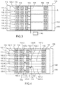
- the figure 4 represents the sensor 100 according to a second embodiment.
- the selection transistors 103 associated with the pixels of the same column are not connected to a single read column 105, but to two read columns 105.1 and 105.2 such as a portion of the pixels 102 d.
- one column are connected to one of the two read columns 105.1 and the other pixels 102 of this column are connected to the other of the two read columns 105.2.
- the selection transistors of the odd pixel lines are connected to a first read column 105.1 and the selection transistors of the even pixel lines (transistors 103.2, 103.4 and 103.6) are connected to a second reading column 105.2.
- the sensor 100 according to this second embodiment comprises a number of read columns 105, and therefore also a number of read circuits 115, corresponding to twice that of the sensor 100 according to this first embodiment.
- the sensor 100 makes it possible to perform a simultaneous reading of two pixel lines 102 advantageously heated by the same portion 111.
- the gates of the selection transistors 103 of the two lines of pixels intended to be read simultaneously are connected to a same selection line 107 making it possible to turn on the selection transistors 103 of these two lines of pixels during a reading of the two lines of pixels.
- This reading sequence is repeated for each next group of two rows of pixels to which one of the portions 111 is associated.
- the heating elements are formed from the same electrically conductive level as that used to form the upper electrodes of the pyroelectric capacitances of the pixels, the portions 111 forming both the heating elements and the upper electrodes of the pixels 102.
- the heating elements are not formed from the same electrically conductive level as that used for producing the upper electrodes.
- the portions 111 and the upper electrodes 110 correspond to distinct elements.
- the portions 111 forming the heating elements of the pixels are covered with a dielectric layer itself covered with an electrically conductive layer which is electrically connected to ground.
- This electrically conductive layer may be covered by the protective layer 109.
- This electrically conductive layer comprising for example an electrically conductive ink, thus forms an electromagnetic shielding between the element whose thermal pattern is intended to be detected, for example a finger in the case of a 100 fingerprint sensor, and the portions 111 forming the polarization electrodes of each pixel 102, thus avoiding the recovery of electromagnetic noise (eg 50 Hz noise from the sector) in the measurements made.
- This electrically conductive layer also protects the sensor 100 against electrostatic discharge (ESD).
- this electromagnetic shielding layer can be disposed directly above the pyroelectric material.
- This electromagnetic shielding layer is covered with a dielectric layer on which the portions 111 forming the heating elements are arranged. In this configuration, the heating elements are well arranged closer to the element whose thermal pattern is detected by the sensor 100.
- the electrically conductive layer forming such a shielding layer is designated 112.
- the thermal pattern detected by the sensor 100 advantageously corresponds to a fingerprint.
- the senor 100 may further comprise an electronic processing circuit adapted to construct an overall image of the thermal pattern from the measurements made at each pixel 102.
- This electronic processing circuit may also be able to compare this image with several images stored in a database in order to identify whether the detected thermal pattern corresponds to one of those stored in the database.
- the electronic processing circuit may also be able to display an image of the detected thermal pattern.
- the portions 111 are heated one by one, by applying a suitable electrical potential on the end 116 of the portion 111 and connecting the end 118 of this portion 111 to ground via the portion 120. to which the ends 118 of all the second portions 111 are connected.
- a suitable electrical potential on the end 116 of the portion 111 and connecting the end 118 of this portion 111 to ground via the portion 120. to which the ends 118 of all the second portions 111 are connected.
- a heating potential is applied to the end 116 of the portion 111.1 and the ends 116 of the other portions 111 (the portions 111.2 and 111.3 in the example of FIG. figure 2 ) are connected to the mass.
- the heating current first passes through the portion 111.1, then the other portions 111 of the sensor serve to evacuate the current to ground.
- the other portions 111 are therefore also subjected to heating, but when the sensor 100 has a large number of rows of pixels, for example a hundred, the current divides in all these other portions 111 which makes this heating in these other portions 111 negligible compared to that achieved by portion 111.1.
- This possibility of using the conductive portions associated with the unread lines of pixels to evacuate the heating current can be applied to other types of sensor, for example to a sensor in which each second portion 111 is associated only with to a single line of pixels.
- the figure 5 represents the sensor 100 according to a third embodiment.
- each of the reading electrodes 108 of these pixel lines 102 is not distinct for each of the pixels 102, but is common to two pixels of the same column which are heated by different portions 111.
- the reading electrodes of two pixels lying on the same column are electrically connected to each other because they are formed by a same portion of electrically conductive material.
- the reading electrodes of the pixels of the same column and belonging to the two pixel lines 102.2 and 102.3, each associated with a different heating element are formed by the same portion of electrically conductive material.
- the reading electrodes of the pixels of the same column and belonging to the two pixel lines 102.4 and 102.5, each associated with a different heating element are formed by the same portion of electrically conductive material.
- this pooling of the reading electrodes makes it possible to reduce the number of selection transistors 103 necessary because only one selection transistor 103 is associated with each of the portions forming the electrodes. reading of at least two pixels. By considering two rows of pixels whose reading electrodes are formed, for each column, by a single electrically conductive portion, a single line of selection transistors 103 is necessary to perform the reading of these two lines of pixels. Moreover, the reduction of the number of selection transistors 103 implies, with respect to the first embodiment, also the reduction of the number of selection lines 107 which are connected to the gates of the selection transistors 103.
Landscapes
- Engineering & Computer Science (AREA)
- Physics & Mathematics (AREA)
- General Physics & Mathematics (AREA)
- Human Computer Interaction (AREA)
- Multimedia (AREA)
- Theoretical Computer Science (AREA)
- Power Engineering (AREA)
- Spectroscopy & Molecular Physics (AREA)
- Photometry And Measurement Of Optical Pulse Characteristics (AREA)
- Radiation Pyrometers (AREA)
Applications Claiming Priority (1)
| Application Number | Priority Date | Filing Date | Title |
|---|---|---|---|
| FR1657389A FR3054696B1 (fr) | 2016-07-29 | 2016-07-29 | Capteur de motif thermique a elements chauffants mutualises |
Publications (2)
| Publication Number | Publication Date |
|---|---|
| EP3276533A2 true EP3276533A2 (de) | 2018-01-31 |
| EP3276533A3 EP3276533A3 (de) | 2018-02-14 |
Family
ID=57750043
Family Applications (1)
| Application Number | Title | Priority Date | Filing Date |
|---|---|---|---|
| EP17183876.6A Withdrawn EP3276533A3 (de) | 2016-07-29 | 2017-07-28 | Wärmemustersensor mit gemeinsam genutzten heizelementen |
Country Status (3)
| Country | Link |
|---|---|
| US (1) | US10489625B2 (de) |
| EP (1) | EP3276533A3 (de) |
| FR (1) | FR3054696B1 (de) |
Cited By (1)
| Publication number | Priority date | Publication date | Assignee | Title |
|---|---|---|---|---|
| FR3108756A1 (fr) * | 2020-03-30 | 2021-10-01 | Commissariat A L'energie Atomique Et Aux Energies Alternatives | Capteur de motif thermique |
Families Citing this family (11)
| Publication number | Priority date | Publication date | Assignee | Title |
|---|---|---|---|---|
| FR3044443B1 (fr) | 2015-11-30 | 2018-12-07 | Commissariat A L'energie Atomique Et Aux Energies Alternatives | Procede de capture de motif thermique |
| FR3044407B1 (fr) | 2015-11-30 | 2020-05-22 | Commissariat A L'energie Atomique Et Aux Energies Alternatives | Capteur de motif thermique |
| FR3046275B1 (fr) | 2015-12-23 | 2018-12-07 | Commissariat A L'energie Atomique Et Aux Energies Alternatives | Capteur d'empreintes a eclairage oled |
| FR3046277B1 (fr) | 2015-12-23 | 2018-02-16 | Commissariat A L'energie Atomique Et Aux Energies Alternatives | Procede pour reconnaitre une fausse empreinte papillaire par eclairage structure |
| FR3054698B1 (fr) | 2016-07-29 | 2018-09-28 | Commissariat A L'energie Atomique Et Aux Energies Alternatives | Capteur de motif thermique actif comprenant une matrice passive de pixels |
| FR3064112B1 (fr) | 2017-03-16 | 2021-06-18 | Commissariat Energie Atomique | Dispositif imageur optique |
| FR3074574B1 (fr) * | 2017-12-04 | 2020-01-03 | Commissariat A L'energie Atomique Et Aux Energies Alternatives | Capteur de motif thermique a capacite pyroelectrique |
| WO2020188313A2 (en) * | 2018-07-10 | 2020-09-24 | Next Biometrics Group Asa | Thermally conductive and protective coating for electronic device |
| CN110045532A (zh) * | 2019-04-30 | 2019-07-23 | 武汉华星光电技术有限公司 | 液晶显示面板 |
| EP4268203A4 (de) * | 2020-12-22 | 2024-08-28 | Fingerprint Cards Anacatum IP AB | Fingerabdrucksensor mit spaltenauslese |
| EP4275219A1 (de) | 2021-01-08 | 2023-11-15 | Borealis AG | Zusammensetzung |
Citations (1)
| Publication number | Priority date | Publication date | Assignee | Title |
|---|---|---|---|---|
| US6091837A (en) * | 1995-04-11 | 2000-07-18 | Dinh; Ngoc Minh | Sensor for acquiring a fingerprint image based on heat transfer |
Family Cites Families (10)
| Publication number | Priority date | Publication date | Assignee | Title |
|---|---|---|---|---|
| US4394773A (en) | 1980-07-21 | 1983-07-19 | Siemens Corporation | Fingerprint sensor |
| US4429413A (en) | 1981-07-30 | 1984-01-31 | Siemens Corporation | Fingerprint sensor |
| GB8325935D0 (en) * | 1983-09-28 | 1983-11-02 | Secr Defence | Thermal detector |
| US5818043A (en) * | 1993-04-09 | 1998-10-06 | Thomson-Csf | Bolometric thermal detector |
| FR2749955B1 (fr) | 1996-06-14 | 1998-09-11 | Thomson Csf | Systeme de lecture d'empreintes digitales |
| DE10222616A1 (de) * | 2002-05-17 | 2003-12-04 | Univ Albert Ludwigs Freiburg | Fingerabdruck-Verifikationsmodul |
| FR2862394B1 (fr) * | 2003-11-18 | 2006-02-17 | Atmel Grenoble Sa | Generateur de sequences binaires aleatoires |
| US9060146B2 (en) * | 2009-01-06 | 2015-06-16 | Next Biometrics Group Asa | Low noise reading architecture for active sensor arrays |
| FR2959657B1 (fr) | 2010-05-06 | 2012-06-22 | Commissariat Energie Atomique | Transducteur de variation temporelle de température, puce électronique incorporant ce transducteur et procédé de fabrication de cette puce |
| EP3020551B1 (de) * | 2013-07-11 | 2018-11-07 | FUJI Corporation | Siebdruckverfahren und siebdruckvorrichtung |
-
2016
- 2016-07-29 FR FR1657389A patent/FR3054696B1/fr active Active
-
2017
- 2017-07-28 EP EP17183876.6A patent/EP3276533A3/de not_active Withdrawn
- 2017-07-28 US US15/662,778 patent/US10489625B2/en active Active
Patent Citations (1)
| Publication number | Priority date | Publication date | Assignee | Title |
|---|---|---|---|---|
| US6091837A (en) * | 1995-04-11 | 2000-07-18 | Dinh; Ngoc Minh | Sensor for acquiring a fingerprint image based on heat transfer |
Cited By (2)
| Publication number | Priority date | Publication date | Assignee | Title |
|---|---|---|---|---|
| FR3108756A1 (fr) * | 2020-03-30 | 2021-10-01 | Commissariat A L'energie Atomique Et Aux Energies Alternatives | Capteur de motif thermique |
| EP3889832A1 (de) * | 2020-03-30 | 2021-10-06 | Commissariat à l'énergie atomique et aux énergies alternatives | Wärmebildsensor |
Also Published As
| Publication number | Publication date |
|---|---|
| FR3054696A1 (fr) | 2018-02-02 |
| US20180032781A1 (en) | 2018-02-01 |
| US10489625B2 (en) | 2019-11-26 |
| EP3276533A3 (de) | 2018-02-14 |
| FR3054696B1 (fr) | 2019-05-17 |
Similar Documents
| Publication | Publication Date | Title |
|---|---|---|
| FR3054697B1 (fr) | Procede de capture de motif thermique a chauffage optimise des pixels | |
| EP3654242B1 (de) | Sensor für aktives wärmemuster, das eine passive pixelmatrix umfasst | |
| EP3384257B1 (de) | Wärmemustersensor | |
| FR3054696A1 (fr) | Capteur de motif thermique a elements chauffants mutualises | |
| EP2012101B1 (de) | Vorrichtung zur Detektion von elektromagnetischer Strahlung, insbesondere von Infrarotstrahlung | |
| EP3384256B1 (de) | Verfahren zur erfassung eines wärmemusters | |
| FR3044408B1 (fr) | Capteur de motif thermique a capacite pyroelectrique horizontale | |
| FR3044409A1 (fr) | Capteur de motif thermique comportant une portion pyroelectrique superieure a forte conductivite thermique | |
| EP3435285B1 (de) | Thermischer sensor mit zwei übereinander angeordneten pyroelektrischen abschnitten für die messung eines ladungsunterschieds | |
| EP3276585B1 (de) | Aktiver temperatursensor, der für grosse pixel geeignet ist | |
| FR3069938A1 (fr) | Dispositif de capture par capsules thermo-resistives adapte a un adressage passif | |
| EP3889832A1 (de) | Wärmebildsensor | |
| EP3767260B1 (de) | Sensor und verfahren zur erfassung eines wärmemusters mit doppelter integration | |
| EP3483787A1 (de) | Verfahren zur durchführung einer stapelung von schichten für einen matrix-wärmesensor | |
| EP3492894A1 (de) | Thermischer mustersensor mit pyroelektrischer kapazität | |
| EP2385485B1 (de) | Verfahren zum kalibrieren eines elektronischen chips und zugehöriges detektor thermischer muster | |
| WO2018042115A1 (fr) | Capteur de motifs thermiques par imagerie infrarouge d'une matrice d'éléments chauffants. |
Legal Events
| Date | Code | Title | Description |
|---|---|---|---|
| PUAI | Public reference made under article 153(3) epc to a published international application that has entered the european phase |
Free format text: ORIGINAL CODE: 0009012 |
|
| STAA | Information on the status of an ep patent application or granted ep patent |
Free format text: STATUS: THE APPLICATION HAS BEEN PUBLISHED |
|
| PUAL | Search report despatched |
Free format text: ORIGINAL CODE: 0009013 |
|
| AK | Designated contracting states |
Kind code of ref document: A2 Designated state(s): AL AT BE BG CH CY CZ DE DK EE ES FI FR GB GR HR HU IE IS IT LI LT LU LV MC MK MT NL NO PL PT RO RS SE SI SK SM TR |
|
| AX | Request for extension of the european patent |
Extension state: BA ME |
|
| AK | Designated contracting states |
Kind code of ref document: A3 Designated state(s): AL AT BE BG CH CY CZ DE DK EE ES FI FR GB GR HR HU IE IS IT LI LT LU LV MC MK MT NL NO PL PT RO RS SE SI SK SM TR |
|
| AX | Request for extension of the european patent |
Extension state: BA ME |
|
| RIC1 | Information provided on ipc code assigned before grant |
Ipc: G06K 9/00 20060101AFI20180111BHEP |
|
| STAA | Information on the status of an ep patent application or granted ep patent |
Free format text: STATUS: REQUEST FOR EXAMINATION WAS MADE |
|
| 17P | Request for examination filed |
Effective date: 20180807 |
|
| RBV | Designated contracting states (corrected) |
Designated state(s): AL AT BE BG CH CY CZ DE DK EE ES FI FR GB GR HR HU IE IS IT LI LT LU LV MC MK MT NL NO PL PT RO RS SE SI SK SM TR |
|
| RAP1 | Party data changed (applicant data changed or rights of an application transferred) |
Owner name: COMMISSARIAT A L'ENERGIE ATOMIQUE ET AUX ENERGIES Owner name: IDEMIA IDENTITY & SECURITY FRANCE |
|
| STAA | Information on the status of an ep patent application or granted ep patent |
Free format text: STATUS: EXAMINATION IS IN PROGRESS |
|
| 17Q | First examination report despatched |
Effective date: 20190827 |
|
| STAA | Information on the status of an ep patent application or granted ep patent |
Free format text: STATUS: THE APPLICATION IS DEEMED TO BE WITHDRAWN |
|
| 18D | Application deemed to be withdrawn |
Effective date: 20200307 |